EP1501104A1 - Circuit imprimé ayant une résistance et procédé de fabrication - Google Patents
Circuit imprimé ayant une résistance et procédé de fabrication Download PDFInfo
- Publication number
- EP1501104A1 EP1501104A1 EP04012945A EP04012945A EP1501104A1 EP 1501104 A1 EP1501104 A1 EP 1501104A1 EP 04012945 A EP04012945 A EP 04012945A EP 04012945 A EP04012945 A EP 04012945A EP 1501104 A1 EP1501104 A1 EP 1501104A1
- Authority
- EP
- European Patent Office
- Prior art keywords
- resistor
- circuit board
- electrical resistance
- resistance value
- conductor
- Prior art date
- Legal status (The legal status is an assumption and is not a legal conclusion. Google has not performed a legal analysis and makes no representation as to the accuracy of the status listed.)
- Withdrawn
Links
Images


Classifications
-
- H—ELECTRICITY
- H01—ELECTRIC ELEMENTS
- H01C—RESISTORS
- H01C17/00—Apparatus or processes specially adapted for manufacturing resistors
- H01C17/22—Apparatus or processes specially adapted for manufacturing resistors adapted for trimming
- H01C17/24—Apparatus or processes specially adapted for manufacturing resistors adapted for trimming by removing or adding resistive material
-
- H—ELECTRICITY
- H05—ELECTRIC TECHNIQUES NOT OTHERWISE PROVIDED FOR
- H05K—PRINTED CIRCUITS; CASINGS OR CONSTRUCTIONAL DETAILS OF ELECTRIC APPARATUS; MANUFACTURE OF ASSEMBLAGES OF ELECTRICAL COMPONENTS
- H05K1/00—Printed circuits
- H05K1/16—Printed circuits incorporating printed electric components, e.g. printed resistors, capacitors or inductors
-
- H—ELECTRICITY
- H01—ELECTRIC ELEMENTS
- H01C—RESISTORS
- H01C17/00—Apparatus or processes specially adapted for manufacturing resistors
- H01C17/22—Apparatus or processes specially adapted for manufacturing resistors adapted for trimming
-
- H—ELECTRICITY
- H05—ELECTRIC TECHNIQUES NOT OTHERWISE PROVIDED FOR
- H05K—PRINTED CIRCUITS; CASINGS OR CONSTRUCTIONAL DETAILS OF ELECTRIC APPARATUS; MANUFACTURE OF ASSEMBLAGES OF ELECTRICAL COMPONENTS
- H05K1/00—Printed circuits
- H05K1/16—Printed circuits incorporating printed electric components, e.g. printed resistors, capacitors or inductors
- H05K1/167—Printed circuits incorporating printed electric components, e.g. printed resistors, capacitors or inductors incorporating printed resistors
-
- H—ELECTRICITY
- H05—ELECTRIC TECHNIQUES NOT OTHERWISE PROVIDED FOR
- H05K—PRINTED CIRCUITS; CASINGS OR CONSTRUCTIONAL DETAILS OF ELECTRIC APPARATUS; MANUFACTURE OF ASSEMBLAGES OF ELECTRICAL COMPONENTS
- H05K2201/00—Indexing scheme relating to printed circuits covered by H05K1/00
- H05K2201/03—Conductive materials
- H05K2201/0332—Structure of the conductor
- H05K2201/0335—Layered conductors or foils
- H05K2201/0347—Overplating, e.g. for reinforcing conductors or bumps; Plating over filled vias
-
- H—ELECTRICITY
- H05—ELECTRIC TECHNIQUES NOT OTHERWISE PROVIDED FOR
- H05K—PRINTED CIRCUITS; CASINGS OR CONSTRUCTIONAL DETAILS OF ELECTRIC APPARATUS; MANUFACTURE OF ASSEMBLAGES OF ELECTRICAL COMPONENTS
- H05K2201/00—Indexing scheme relating to printed circuits covered by H05K1/00
- H05K2201/03—Conductive materials
- H05K2201/0332—Structure of the conductor
- H05K2201/0335—Layered conductors or foils
- H05K2201/035—Paste overlayer, i.e. conductive paste or solder paste over conductive layer
-
- H—ELECTRICITY
- H05—ELECTRIC TECHNIQUES NOT OTHERWISE PROVIDED FOR
- H05K—PRINTED CIRCUITS; CASINGS OR CONSTRUCTIONAL DETAILS OF ELECTRIC APPARATUS; MANUFACTURE OF ASSEMBLAGES OF ELECTRICAL COMPONENTS
- H05K2203/00—Indexing scheme relating to apparatus or processes for manufacturing printed circuits covered by H05K3/00
- H05K2203/17—Post-manufacturing processes
- H05K2203/171—Tuning, e.g. by trimming of printed components or high frequency circuits
Definitions
- the present invention relates to a circuit board having a resistor, formed thereon with resistor paste, of which the electrical resistance is adjustable, and a method for manufacturing such a circuit board. More specifically, this invention relates to a circuit board having a resistor formed thereon of which the electrical resistance is accurately adjustable without damaging the circuit board.
- circuit board product carrying a semiconductor element thereon, in which a resistor is formed in the circuit board by, for example, printing resistor paste such as carbon paste on the circuit board itself.
- resistor paste such as carbon paste
- the resistor is formed by a screen printing method, carbon paste is coated on the circuit board in accordance with a predetermined pattern and heated at a suitable temperature for hardening the carbon paste.
- the laser trimming method for adjusting the resistance value of the resistor is a method for correcting the electrical resistance value of the resistor to a required value by irradiating a laser beam onto the resistor formed on the circuit board to partially narrow the resistor.
- a technique for trimming the resistor, with high accuracy and within a short time has been developed.
- micro-cracks generated in the resistor during the laser trimming may vary the electrical resistance value of the resistor over time.
- the present invention has been made to solve such problems and an object thereof is to provide a circuit board in which the electrical resistance value of a resistor is accurately adjusted and is high in reliability and free from a change with time, and a method for producing such a circuit board.
- the present invention is as follows:
- a method for producing a circuit board comprising a process for forming a circuit pattern on the surface of a circuit board, a process for printing a resistor between electrodes in the circuit pattern with resistor paste, a process for measuring the electrical resistance value of the resistor, and a process for forming a conductor, of a predetermined area for adjusting the electrical resistance value, having a conductivity higher than that of the resistor on the surface of the resistor if the measured electrical resistance value is outside the designed tolerance thereof.
- a conductive paste is coated in a predetermined area on the surface of the resistor.
- a conductor is preferably plated in a predetermined area on the surface of the resistor.
- the conductor for adjusting the electrical resistance value can be formed by using a conventional plating device, the electrical resistance value is adjustable with only a small increase in production cost without the necessity of a novel installation therefor.
- a plurality of conductor spots can be attached onto the surface of the resistor by ink jet processing.
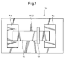
- Fig. 1 is an enlarged plan view of part of a circuit board in which a resistor is formed. As shown in Fig. 1, a resistor 16 is provided between a pair of electrodes 14a and 14a having a predetermined width in accordance with a predetermined pattern on the surface of a circuit board 10.
- the resistor 16 of this embodiment is formed by printing carbon paste of an epoxy resin-type carbon black mixed with a conductive filler.
- the electrical resistance value of the resistor 16 is determined by the distance between the electrodes 14a and 14a, the width and the thickness of the resistor 16, and the resistance value of the paste used in the resistor 16. Accordingly, when the resistor 16 is formed in the circuit board 10, the distance between the electrodes 14a and 14a, the width and the thickness of the resistor 16 are set to match the resistance value of the paste used for the respective resistors 16 while using a mask pattern or other method.
- the circuit board 10 is manufactured by forming a circuit pattern 14 and the electrodes 14a, 14a in accordance with a predetermined pattern by a known method for forming any circuit board, such as a subtractive process.
- Fig. 2 is a flow chart schematically illustrating the production steps of the circuit board according to one embodiment of the present invention
- Figs. 3(a) to 3(g) are illustrations of the circuit board in the respective steps in Fig. 2.
- a one-side copper-clad board 13 is prepared by adhering a copper foil 12 on one of the surfaces of a resinous board 11.
- the one-side copper-clad board 13 is covered with a resist 20 (step 1).
- the resist 20 is exposed to light in accordance with a circuit pattern and developed to form a resist pattern 20a in which portions to be a circuit pattern are concealed as shown in Fig. 3(c) (step 2).
- step 3 part of the copper foil 12 exposed from the resist pattern 20a is removed by the etching as shown in Fig. 3(d) (step 3).
- the resist pattern 20a is etched with a solvent for the resist and removed (step 4).
- Fig. 3(e) shows a state in which the resist pattern 20a has been removed.
- the predetermined circuit pattern 14 is formed on the resinous board 11.
- resistor 16 is formed on the surface of the circuit board 10
- the resistor 16 is formed, as shown in Fig. 3(f), on the resinous board 11 on which the circuit pattern is formed.
- Reference numeral 14a denotes a pair of electrodes between which the resistor is formed.
- the resistor 16 is formed by printing carbon paste while using a mask having a slit of a predetermined width (step 5).
- the carbon paste is coated between the electrodes 14a and 14a so that opposite ends thereof are overlapped with the electrodes as shown in Fig. 1. After being coated, the carbon paste is heated and hardened to become the resistor 16 (step 6).
- a shape of the resistor 16 is not always exactly the same every time even if the same slit in the same mask is used for coating the carbon paste because the composition of carbon paste material may vary or the coating operation may fluctuate.
- Figs. 4(a) and 4(b) are illustrations of shapes of the resistor formed in the circuit board.
- Fig. 4(a) is a plan view and Fig. 4(b) a side view of Fig. 4(a) as seen in the direction shown by an arrow.
- a broken line indicates a designed shape of the resistor 16
- a solid line indicates an actually formed shape of the resistor 16.
- the shape of the actually formed resistor 16 by printing the carbon paste is often different from the designed shape, whereby the electrical resistance value of the resistor 16 may be larger than the designed or reference electrical resistance value.
- the electrical resistance value of the resistor 16 is adjustable according to this embodiment to improve the yield of the circuit board 10.
- the electrical resistances of the respective resistors are measured (step 7) to calculate the difference from the designed value (step 8).
- conductor 18, such as gold, nickel or alloys thereof, having a conductivity higher than that of the resistor 16 is attached onto the surface of the resistor 16 as shown in Fig. 3(g) to adjust the electrical resistance value (step 9).
- a method for attaching the conductor 18 to the surface of the resistor for the adjustment of the electrical resistance includes, for example, one in which the conductive paste is coated on the surface of the resistor 16 at a predetermined width by an ink jet, one in which the conductor 18 for the adjustment of the electrical resistance is plated on the surface of the resistor 16, and one in which a conductive piece having a predetermined width is adhered onto the surface of the resistor 16.
- Each of them may be suitably selected in accordance with the production process of the circuit board 10.
- the conductor 18 for the adjustment of the electrical resistance is plated to cross the resistor 16 in the widthwise direction.
- the electrical resistance value of a portion of the resistor 16 where the conductor 18 is formed becomes zero, which means that the length of the resistor 16 is substantially shortened and thus the electrical resistance value is reduced to an extent corresponding thereto.
- Fig. 5 illustrates another embodiment in which the conductors 18, 18a for the adjustment of the electrical resistance are formed in a spotted manner on the surface of the resistor 16.
- the conductor 18a may be provided not only to cross the resistor 16 in the widthwise direction but also to vary its area.
- the conductors 18, 18a for the adjustment of the electrical resistance are provided while adjusting the area thereof on the surface of the resistor 16 based on the measured result of the electrical resistance value of the respective resistor 16.
- efficient adjustment is possible because the conductive paste is suitably coated based on the measured electrical resistance value of the respective resistor 16.
- the size of the individual spotted conductors 18, 18a and the number of such conductors can be selected so as to obtain a suitable adjustment of the electrical resistance value.
- the conductor 18 for the adjustment of the electrical resistance is formed on the surface of the resistor 16 to adjust the resistor 16 to have the predetermined electrical resistance value.
- the conductor 18 for the adjustment of the electrical resistance is preferably formed in the widthwise direction.
- the conductor 18 for the adjustment of the electrical resistance is preferably formed in the lengthwise direction.
- the circuit board having the designed electric characteristics As the electrical resistance of the resistor in the circuit board is measured and adjusted, the circuit board having the designed electric characteristics is provided.
- the adjustment of the resistor is carried out by the plating, it is possible to use a process for manufacturing a multi-layered circuit board, provided an other proper process is combined therewith, whereby the adjustment may be effectively carried out.
Landscapes
- Engineering & Computer Science (AREA)
- Microelectronics & Electronic Packaging (AREA)
- Manufacturing & Machinery (AREA)
- Parts Printed On Printed Circuit Boards (AREA)
Applications Claiming Priority (2)
| Application Number | Priority Date | Filing Date | Title |
|---|---|---|---|
| JP2003169627A JP2005005599A (ja) | 2003-06-13 | 2003-06-13 | 配線基板および配線基板の製造方法 |
| JP2003169627 | 2003-06-13 |
Publications (1)
| Publication Number | Publication Date |
|---|---|
| EP1501104A1 true EP1501104A1 (fr) | 2005-01-26 |
Family
ID=33487603
Family Applications (1)
| Application Number | Title | Priority Date | Filing Date |
|---|---|---|---|
| EP04012945A Withdrawn EP1501104A1 (fr) | 2003-06-13 | 2004-06-01 | Circuit imprimé ayant une résistance et procédé de fabrication |
Country Status (5)
| Country | Link |
|---|---|
| US (1) | US7423513B2 (fr) |
| EP (1) | EP1501104A1 (fr) |
| JP (1) | JP2005005599A (fr) |
| KR (1) | KR20040107433A (fr) |
| CN (1) | CN1575095A (fr) |
Families Citing this family (6)
| Publication number | Priority date | Publication date | Assignee | Title |
|---|---|---|---|---|
| JP4792761B2 (ja) * | 2005-02-16 | 2011-10-12 | 凸版印刷株式会社 | 抵抗素子の形成方法 |
| KR100908629B1 (ko) * | 2007-11-27 | 2009-07-21 | 삼성전기주식회사 | 저항체 제조방법 |
| US8686292B2 (en) | 2011-02-23 | 2014-04-01 | Miraco, Inc. | Tunable resistance conductive ink circuit |
| KR102628153B1 (ko) * | 2015-11-17 | 2024-01-23 | 필립모리스 프로덕츠 에스.에이. | 맞춤형 식별 저항을 갖는 에어로졸 발생 시스템용 카트리지 |
| CN110223811A (zh) * | 2019-04-23 | 2019-09-10 | 深圳市金瑞电子材料有限公司 | 二次安全保护元件的制造方法、芯片及设备 |
| CN115691918B (zh) * | 2022-11-11 | 2025-11-18 | 珠海杰赛科技有限公司 | 薄膜电阻阻值调整方法及系统、pcb电路板、印制设备 |
Citations (3)
| Publication number | Priority date | Publication date | Assignee | Title |
|---|---|---|---|---|
| GB522660A (en) * | 1937-12-18 | 1940-06-24 | Fides Gmbh | Improvements in or relating to electrical resistances |
| DE4026220A1 (de) * | 1990-08-18 | 1992-02-20 | Blaupunkt Werke Gmbh | Verfahren zum abgleich von gedruckten widerstaenden |
| US5621240A (en) * | 1995-09-05 | 1997-04-15 | Delco Electronics Corp. | Segmented thick film resistors |
Family Cites Families (5)
| Publication number | Priority date | Publication date | Assignee | Title |
|---|---|---|---|---|
| US3909680A (en) * | 1973-02-16 | 1975-09-30 | Matsushita Electric Industrial Co Ltd | Printed circuit board with silver migration prevention |
| US4035613A (en) * | 1976-01-08 | 1977-07-12 | Kyoto Ceramic Co., Ltd. | Cylindrical ceramic heating device |
| DE4343934B4 (de) * | 1992-12-22 | 2005-08-25 | Denso Corp., Kariya | Verfahren zum Erzeugen von Vielfach-Dickschichtsubstraten |
| JP2001085207A (ja) | 1999-09-10 | 2001-03-30 | Rohm Co Ltd | チップ抵抗器におけるレーザトリミング方法 |
| US6897761B2 (en) * | 2002-12-04 | 2005-05-24 | Cts Corporation | Ball grid array resistor network |
-
2003
- 2003-06-13 JP JP2003169627A patent/JP2005005599A/ja active Pending
-
2004
- 2004-05-28 US US10/855,342 patent/US7423513B2/en not_active Expired - Fee Related
- 2004-06-01 EP EP04012945A patent/EP1501104A1/fr not_active Withdrawn
- 2004-06-09 CN CNA2004100479652A patent/CN1575095A/zh active Pending
- 2004-06-12 KR KR1020040043286A patent/KR20040107433A/ko not_active Ceased
Patent Citations (3)
| Publication number | Priority date | Publication date | Assignee | Title |
|---|---|---|---|---|
| GB522660A (en) * | 1937-12-18 | 1940-06-24 | Fides Gmbh | Improvements in or relating to electrical resistances |
| DE4026220A1 (de) * | 1990-08-18 | 1992-02-20 | Blaupunkt Werke Gmbh | Verfahren zum abgleich von gedruckten widerstaenden |
| US5621240A (en) * | 1995-09-05 | 1997-04-15 | Delco Electronics Corp. | Segmented thick film resistors |
Non-Patent Citations (1)
| Title |
|---|
| PATENT ABSTRACTS OF JAPAN vol. 0161, no. 88 (E - 1198) 7 May 1992 (1992-05-07) * |
Also Published As
| Publication number | Publication date |
|---|---|
| KR20040107433A (ko) | 2004-12-20 |
| JP2005005599A (ja) | 2005-01-06 |
| CN1575095A (zh) | 2005-02-02 |
| US7423513B2 (en) | 2008-09-09 |
| US20040252010A1 (en) | 2004-12-16 |
Similar Documents
| Publication | Publication Date | Title |
|---|---|---|
| US8686828B2 (en) | Resistor and method for making same | |
| US7667568B2 (en) | Chip resistor and manufacturing method thereof | |
| US4629681A (en) | Method of manufacturing multilayer circuit board | |
| US20050196966A1 (en) | Method for fabricating embedded thin film resistors of printed circuit board | |
| CN100499963C (zh) | 具有电阻器的线路板及其制造方法 | |
| US7038571B2 (en) | Polymer thick film resistor, layout cell, and method | |
| US7423513B2 (en) | Circuit board having resistor and method for manufacturing the circuit board | |
| US6280907B1 (en) | Process for forming polymer thick film resistors and metal thin film resistors on a printed circuit substrate | |
| US20020013997A1 (en) | Method of manufacture of integral low and high value resistors on a printed circuit board | |
| US4446355A (en) | Crossover construction of thermal-head and method of manufacturing same | |
| JP5262159B2 (ja) | 薄膜チップ抵抗器の製造方法 | |
| US9113546B2 (en) | Method for manufacturing electric film body | |
| KR100714354B1 (ko) | 인쇄회로기판의 임베디드 박막 저항기의 제조 방법 | |
| JPH07335411A (ja) | チップ型抵抗ネットワーク | |
| JP2004023094A (ja) | 内蔵レジスタを有するプリント回路基板、その製造方法及びその最適化方法 | |
| CN118053639A (zh) | 厚膜电阻元件及其制作方法 | |
| JPH10163003A (ja) | チップ抵抗器 | |
| JPH09251908A (ja) | チップネットワーク抵抗器 | |
| JPH09167701A (ja) | チップ型抵抗ネットワーク | |
| JPH07326506A (ja) | チップ抵抗器の製造方法 | |
| JPH07202376A (ja) | 抵抗体を有する回路基板 | |
| JP2007067149A (ja) | 回路配線基板及びその製造方法 | |
| JPH04250682A (ja) | 混成集積回路用基板とその製造方法 |
Legal Events
| Date | Code | Title | Description |
|---|---|---|---|
| PUAI | Public reference made under article 153(3) epc to a published international application that has entered the european phase |
Free format text: ORIGINAL CODE: 0009012 |
|
| AK | Designated contracting states |
Kind code of ref document: A1 Designated state(s): AT BE BG CH CY CZ DE DK EE ES FI FR GB GR HU IE IT LI LU MC NL PL PT RO SE SI SK TR |
|
| AX | Request for extension of the european patent |
Extension state: AL HR LT LV MK |
|
| AKX | Designation fees paid | ||
| REG | Reference to a national code |
Ref country code: DE Ref legal event code: 8566 |
|
| STAA | Information on the status of an ep patent application or granted ep patent |
Free format text: STATUS: THE APPLICATION IS DEEMED TO BE WITHDRAWN |
|
| 18D | Application deemed to be withdrawn |
Effective date: 20050727 |