EP1500922A2 - Elektrolumineszenzgassensor und verfahren zum gasnachweis - Google Patents
Elektrolumineszenzgassensor und verfahren zum gasnachweis Download PDFInfo
- Publication number
- EP1500922A2 EP1500922A2 EP04017327A EP04017327A EP1500922A2 EP 1500922 A2 EP1500922 A2 EP 1500922A2 EP 04017327 A EP04017327 A EP 04017327A EP 04017327 A EP04017327 A EP 04017327A EP 1500922 A2 EP1500922 A2 EP 1500922A2
- Authority
- EP
- European Patent Office
- Prior art keywords
- electroluminescence device
- gas
- ambient atmosphere
- dark spot
- gas sensor
- Prior art date
- Legal status (The legal status is an assumption and is not a legal conclusion. Google has not performed a legal analysis and makes no representation as to the accuracy of the status listed.)
- Withdrawn
Links
- 238000001514 detection method Methods 0.000 title abstract description 47
- 238000005401 electroluminescence Methods 0.000 claims abstract description 338
- 239000012298 atmosphere Substances 0.000 claims abstract description 113
- 238000000034 method Methods 0.000 claims abstract description 51
- 239000007789 gas Substances 0.000 claims description 303
- 238000003860 storage Methods 0.000 claims description 174
- 238000007789 sealing Methods 0.000 claims description 51
- 239000000758 substrate Substances 0.000 claims description 39
- 239000011261 inert gas Substances 0.000 claims description 31
- 238000002161 passivation Methods 0.000 claims description 31
- 238000011049 filling Methods 0.000 claims description 26
- 230000007246 mechanism Effects 0.000 claims description 22
- 230000015572 biosynthetic process Effects 0.000 claims description 14
- 238000007254 oxidation reaction Methods 0.000 claims description 7
- 238000002955 isolation Methods 0.000 claims description 6
- 230000003647 oxidation Effects 0.000 claims description 6
- 230000003247 decreasing effect Effects 0.000 claims description 5
- 230000001590 oxidative effect Effects 0.000 claims description 5
- 239000010410 layer Substances 0.000 description 73
- 239000000463 material Substances 0.000 description 59
- XLYOFNOQVPJJNP-UHFFFAOYSA-N water Substances O XLYOFNOQVPJJNP-UHFFFAOYSA-N 0.000 description 30
- 238000005259 measurement Methods 0.000 description 25
- 239000010408 film Substances 0.000 description 21
- 229910052751 metal Inorganic materials 0.000 description 18
- 239000002184 metal Substances 0.000 description 18
- 230000008859 change Effects 0.000 description 15
- QVGXLLKOCUKJST-UHFFFAOYSA-N atomic oxygen Chemical compound [O] QVGXLLKOCUKJST-UHFFFAOYSA-N 0.000 description 11
- 239000001301 oxygen Substances 0.000 description 11
- 229910052760 oxygen Inorganic materials 0.000 description 11
- 230000001681 protective effect Effects 0.000 description 11
- 229920005989 resin Polymers 0.000 description 11
- 239000011347 resin Substances 0.000 description 11
- 238000002347 injection Methods 0.000 description 9
- 239000007924 injection Substances 0.000 description 9
- 239000000203 mixture Substances 0.000 description 8
- -1 polyphenylene vinylene Polymers 0.000 description 8
- 229910052782 aluminium Inorganic materials 0.000 description 7
- XAGFODPZIPBFFR-UHFFFAOYSA-N aluminium Chemical compound [Al] XAGFODPZIPBFFR-UHFFFAOYSA-N 0.000 description 7
- 230000007423 decrease Effects 0.000 description 7
- 150000002739 metals Chemical class 0.000 description 6
- RYGMFSIKBFXOCR-UHFFFAOYSA-N Copper Chemical compound [Cu] RYGMFSIKBFXOCR-UHFFFAOYSA-N 0.000 description 5
- 229910045601 alloy Inorganic materials 0.000 description 5
- 239000000956 alloy Substances 0.000 description 5
- 229910052802 copper Inorganic materials 0.000 description 5
- 239000010949 copper Substances 0.000 description 5
- 230000005281 excited state Effects 0.000 description 5
- 230000005525 hole transport Effects 0.000 description 5
- 229910052757 nitrogen Inorganic materials 0.000 description 5
- 239000011241 protective layer Substances 0.000 description 5
- BQCADISMDOOEFD-UHFFFAOYSA-N Silver Chemical compound [Ag] BQCADISMDOOEFD-UHFFFAOYSA-N 0.000 description 4
- 238000010586 diagram Methods 0.000 description 4
- 230000000694 effects Effects 0.000 description 4
- 238000000605 extraction Methods 0.000 description 4
- 239000002861 polymer material Substances 0.000 description 4
- 229920000123 polythiophene Polymers 0.000 description 4
- 230000002829 reductive effect Effects 0.000 description 4
- 229910052709 silver Inorganic materials 0.000 description 4
- 239000004332 silver Substances 0.000 description 4
- VYZAMTAEIAYCRO-UHFFFAOYSA-N Chromium Chemical compound [Cr] VYZAMTAEIAYCRO-UHFFFAOYSA-N 0.000 description 3
- FYYHWMGAXLPEAU-UHFFFAOYSA-N Magnesium Chemical compound [Mg] FYYHWMGAXLPEAU-UHFFFAOYSA-N 0.000 description 3
- NRCMAYZCPIVABH-UHFFFAOYSA-N Quinacridone Chemical class N1C2=CC=CC=C2C(=O)C2=C1C=C1C(=O)C3=CC=CC=C3NC1=C2 NRCMAYZCPIVABH-UHFFFAOYSA-N 0.000 description 3
- 239000000853 adhesive Substances 0.000 description 3
- 230000001070 adhesive effect Effects 0.000 description 3
- 230000008901 benefit Effects 0.000 description 3
- 239000003795 chemical substances by application Substances 0.000 description 3
- 229910052804 chromium Inorganic materials 0.000 description 3
- 239000011651 chromium Substances 0.000 description 3
- 239000007772 electrode material Substances 0.000 description 3
- 239000011521 glass Substances 0.000 description 3
- 230000005283 ground state Effects 0.000 description 3
- 229910052749 magnesium Inorganic materials 0.000 description 3
- 239000011777 magnesium Substances 0.000 description 3
- 239000011159 matrix material Substances 0.000 description 3
- 150000002736 metal compounds Chemical class 0.000 description 3
- 229920000642 polymer Polymers 0.000 description 3
- 239000010409 thin film Substances 0.000 description 3
- 238000002834 transmittance Methods 0.000 description 3
- 229910001316 Ag alloy Inorganic materials 0.000 description 2
- XKRFYHLGVUSROY-UHFFFAOYSA-N Argon Chemical compound [Ar] XKRFYHLGVUSROY-UHFFFAOYSA-N 0.000 description 2
- 229910000846 In alloy Inorganic materials 0.000 description 2
- PXHVJJICTQNCMI-UHFFFAOYSA-N Nickel Chemical compound [Ni] PXHVJJICTQNCMI-UHFFFAOYSA-N 0.000 description 2
- XUIMIQQOPSSXEZ-UHFFFAOYSA-N Silicon Chemical compound [Si] XUIMIQQOPSSXEZ-UHFFFAOYSA-N 0.000 description 2
- RTAQQCXQSZGOHL-UHFFFAOYSA-N Titanium Chemical compound [Ti] RTAQQCXQSZGOHL-UHFFFAOYSA-N 0.000 description 2
- XLOMVQKBTHCTTD-UHFFFAOYSA-N Zinc monoxide Chemical compound [Zn]=O XLOMVQKBTHCTTD-UHFFFAOYSA-N 0.000 description 2
- 230000009471 action Effects 0.000 description 2
- 230000004888 barrier function Effects 0.000 description 2
- 239000000872 buffer Substances 0.000 description 2
- 239000000919 ceramic Substances 0.000 description 2
- UUAGAQFQZIEFAH-UHFFFAOYSA-N chlorotrifluoroethylene Chemical group FC(F)=C(F)Cl UUAGAQFQZIEFAH-UHFFFAOYSA-N 0.000 description 2
- 238000004140 cleaning Methods 0.000 description 2
- 150000001875 compounds Chemical class 0.000 description 2
- 230000007547 defect Effects 0.000 description 2
- 230000007850 degeneration Effects 0.000 description 2
- QDGONURINHVBEW-UHFFFAOYSA-N dichlorodifluoroethylene Chemical group FC(F)=C(Cl)Cl QDGONURINHVBEW-UHFFFAOYSA-N 0.000 description 2
- 239000002019 doping agent Substances 0.000 description 2
- 238000000313 electron-beam-induced deposition Methods 0.000 description 2
- PCHJSUWPFVWCPO-UHFFFAOYSA-N gold Chemical compound [Au] PCHJSUWPFVWCPO-UHFFFAOYSA-N 0.000 description 2
- 229910052737 gold Inorganic materials 0.000 description 2
- 239000010931 gold Substances 0.000 description 2
- RBTKNAXYKSUFRK-UHFFFAOYSA-N heliogen blue Chemical compound [Cu].[N-]1C2=C(C=CC=C3)C3=C1N=C([N-]1)C3=CC=CC=C3C1=NC([N-]1)=C(C=CC=C3)C3=C1N=C([N-]1)C3=CC=CC=C3C1=N2 RBTKNAXYKSUFRK-UHFFFAOYSA-N 0.000 description 2
- 238000003384 imaging method Methods 0.000 description 2
- 229910010272 inorganic material Inorganic materials 0.000 description 2
- 239000011147 inorganic material Substances 0.000 description 2
- 238000007733 ion plating Methods 0.000 description 2
- PQXKHYXIUOZZFA-UHFFFAOYSA-M lithium fluoride Chemical compound [Li+].[F-] PQXKHYXIUOZZFA-UHFFFAOYSA-M 0.000 description 2
- SJCKRGFTWFGHGZ-UHFFFAOYSA-N magnesium silver Chemical compound [Mg].[Ag] SJCKRGFTWFGHGZ-UHFFFAOYSA-N 0.000 description 2
- 229910044991 metal oxide Inorganic materials 0.000 description 2
- 150000004706 metal oxides Chemical class 0.000 description 2
- 150000004767 nitrides Chemical class 0.000 description 2
- 229920000620 organic polymer Polymers 0.000 description 2
- 125000002080 perylenyl group Chemical group C1(=CC=C2C=CC=C3C4=CC=CC5=CC=CC(C1=C23)=C45)* 0.000 description 2
- 239000004033 plastic Substances 0.000 description 2
- 229920003023 plastic Polymers 0.000 description 2
- BASFCYQUMIYNBI-UHFFFAOYSA-N platinum Chemical compound [Pt] BASFCYQUMIYNBI-UHFFFAOYSA-N 0.000 description 2
- 229920000767 polyaniline Polymers 0.000 description 2
- 238000012545 processing Methods 0.000 description 2
- 230000035945 sensitivity Effects 0.000 description 2
- 239000010703 silicon Substances 0.000 description 2
- 229910052710 silicon Inorganic materials 0.000 description 2
- VYPSYNLAJGMNEJ-UHFFFAOYSA-N silicon dioxide Inorganic materials O=[Si]=O VYPSYNLAJGMNEJ-UHFFFAOYSA-N 0.000 description 2
- 239000002356 single layer Substances 0.000 description 2
- 238000004544 sputter deposition Methods 0.000 description 2
- 239000010936 titanium Substances 0.000 description 2
- 229910052719 titanium Inorganic materials 0.000 description 2
- 238000007740 vapor deposition Methods 0.000 description 2
- YGLVWOUNCXBPJF-UHFFFAOYSA-N (2,3,4,5-tetraphenylcyclopenta-1,4-dien-1-yl)benzene Chemical compound C1=CC=CC=C1C1C(C=2C=CC=CC=2)=C(C=2C=CC=CC=2)C(C=2C=CC=CC=2)=C1C1=CC=CC=C1 YGLVWOUNCXBPJF-UHFFFAOYSA-N 0.000 description 1
- JCXLYAWYOTYWKM-UHFFFAOYSA-N (2,3,4-triphenylcyclopenta-1,3-dien-1-yl)benzene Chemical compound C1C(C=2C=CC=CC=2)=C(C=2C=CC=CC=2)C(C=2C=CC=CC=2)=C1C1=CC=CC=C1 JCXLYAWYOTYWKM-UHFFFAOYSA-N 0.000 description 1
- KLCLIOISYBHYDZ-UHFFFAOYSA-N 1,4,4-triphenylbuta-1,3-dienylbenzene Chemical compound C=1C=CC=CC=1C(C=1C=CC=CC=1)=CC=C(C=1C=CC=CC=1)C1=CC=CC=C1 KLCLIOISYBHYDZ-UHFFFAOYSA-N 0.000 description 1
- FKEASPXDTWVHGF-UHFFFAOYSA-N 10-hydroxy-1h-benzo[h]quinolin-2-one Chemical compound C1=CC(=O)NC2=C3C(O)=CC=CC3=CC=C21 FKEASPXDTWVHGF-UHFFFAOYSA-N 0.000 description 1
- MGADZUXDNSDTHW-UHFFFAOYSA-N 2H-pyran Chemical compound C1OC=CC=C1 MGADZUXDNSDTHW-UHFFFAOYSA-N 0.000 description 1
- ITLNEDSJKJRPMZ-UHFFFAOYSA-N 8-hydroxy-4-methylquinoline-5-carbonitrile Chemical class C1=CC(C#N)=C2C(C)=CC=NC2=C1O ITLNEDSJKJRPMZ-UHFFFAOYSA-N 0.000 description 1
- 229910000838 Al alloy Inorganic materials 0.000 description 1
- 229910001148 Al-Li alloy Inorganic materials 0.000 description 1
- IJGRMHOSHXDMSA-UHFFFAOYSA-N Atomic nitrogen Chemical compound N#N IJGRMHOSHXDMSA-UHFFFAOYSA-N 0.000 description 1
- OOQAPGNOZVHVDM-UHFFFAOYSA-N CC(C)(C)[Cu](C(C)(C)C)(C(C)(C)C)C(C)(C)C Chemical compound CC(C)(C)[Cu](C(C)(C)C)(C(C)(C)C)C(C)(C)C OOQAPGNOZVHVDM-UHFFFAOYSA-N 0.000 description 1
- 229910000882 Ca alloy Inorganic materials 0.000 description 1
- OYPRJOBELJOOCE-UHFFFAOYSA-N Calcium Chemical compound [Ca] OYPRJOBELJOOCE-UHFFFAOYSA-N 0.000 description 1
- 229910000881 Cu alloy Inorganic materials 0.000 description 1
- XDTMQSROBMDMFD-UHFFFAOYSA-N Cyclohexane Chemical compound C1CCCCC1 XDTMQSROBMDMFD-UHFFFAOYSA-N 0.000 description 1
- KRHYYFGTRYWZRS-UHFFFAOYSA-M Fluoride anion Chemical compound [F-] KRHYYFGTRYWZRS-UHFFFAOYSA-M 0.000 description 1
- YCKRFDGAMUMZLT-UHFFFAOYSA-N Fluorine atom Chemical compound [F] YCKRFDGAMUMZLT-UHFFFAOYSA-N 0.000 description 1
- DGAQECJNVWCQMB-PUAWFVPOSA-M Ilexoside XXIX Chemical compound C[C@@H]1CC[C@@]2(CC[C@@]3(C(=CC[C@H]4[C@]3(CC[C@@H]5[C@@]4(CC[C@@H](C5(C)C)OS(=O)(=O)[O-])C)C)[C@@H]2[C@]1(C)O)C)C(=O)O[C@H]6[C@@H]([C@H]([C@@H]([C@H](O6)CO)O)O)O.[Na+] DGAQECJNVWCQMB-PUAWFVPOSA-M 0.000 description 1
- 229910000799 K alloy Inorganic materials 0.000 description 1
- WHXSMMKQMYFTQS-UHFFFAOYSA-N Lithium Chemical compound [Li] WHXSMMKQMYFTQS-UHFFFAOYSA-N 0.000 description 1
- 229910000861 Mg alloy Inorganic materials 0.000 description 1
- ZOKXTWBITQBERF-UHFFFAOYSA-N Molybdenum Chemical compound [Mo] ZOKXTWBITQBERF-UHFFFAOYSA-N 0.000 description 1
- CBENFWSGALASAD-UHFFFAOYSA-N Ozone Chemical compound [O-][O+]=O CBENFWSGALASAD-UHFFFAOYSA-N 0.000 description 1
- YGYAWVDWMABLBF-UHFFFAOYSA-N Phosgene Chemical compound ClC(Cl)=O YGYAWVDWMABLBF-UHFFFAOYSA-N 0.000 description 1
- 239000004962 Polyamide-imide Substances 0.000 description 1
- 239000004721 Polyphenylene oxide Substances 0.000 description 1
- 239000004734 Polyphenylene sulfide Substances 0.000 description 1
- KJTLSVCANCCWHF-UHFFFAOYSA-N Ruthenium Chemical compound [Ru] KJTLSVCANCCWHF-UHFFFAOYSA-N 0.000 description 1
- ATJFFYVFTNAWJD-UHFFFAOYSA-N Tin Chemical compound [Sn] ATJFFYVFTNAWJD-UHFFFAOYSA-N 0.000 description 1
- NRTOMJZYCJJWKI-UHFFFAOYSA-N Titanium nitride Chemical compound [Ti]#N NRTOMJZYCJJWKI-UHFFFAOYSA-N 0.000 description 1
- 239000007983 Tris buffer Substances 0.000 description 1
- JFBZPFYRPYOZCQ-UHFFFAOYSA-N [Li].[Al] Chemical compound [Li].[Al] JFBZPFYRPYOZCQ-UHFFFAOYSA-N 0.000 description 1
- JHYLKGDXMUDNEO-UHFFFAOYSA-N [Mg].[In] Chemical compound [Mg].[In] JHYLKGDXMUDNEO-UHFFFAOYSA-N 0.000 description 1
- 230000002745 absorbent Effects 0.000 description 1
- 239000002250 absorbent Substances 0.000 description 1
- 229910052783 alkali metal Inorganic materials 0.000 description 1
- 150000001340 alkali metals Chemical class 0.000 description 1
- 229910052784 alkaline earth metal Inorganic materials 0.000 description 1
- 230000004075 alteration Effects 0.000 description 1
- IMALFSHRMABADU-UHFFFAOYSA-K aluminum 4-(4-cyanophenyl)phenolate 2-methyl-5-(trifluoromethyl)quinolin-8-olate Chemical class [Al+3].C(#N)C1=CC=C(C=C1)C1=CC=C(C=C1)[O-].CC1=NC2=C(C=CC(=C2C=C1)C(F)(F)F)[O-].CC1=NC2=C(C=CC(=C2C=C1)C(F)(F)F)[O-] IMALFSHRMABADU-UHFFFAOYSA-K 0.000 description 1
- WJNWGMBCKFIFDS-UHFFFAOYSA-K aluminum 4-methyl-5-(trifluoromethyl)quinolin-8-olate Chemical class [Al+3].CC1=CC=NC2=C(C=CC(=C12)C(F)(F)F)[O-].CC1=CC=NC2=C(C=CC(=C12)C(F)(F)F)[O-].CC1=CC=NC2=C(C=CC(=C12)C(F)(F)F)[O-] WJNWGMBCKFIFDS-UHFFFAOYSA-K 0.000 description 1
- KLTCKTRTUHFMFN-UHFFFAOYSA-K aluminum 5-cyano-2-methylquinolin-8-olate 4-(4-cyanophenyl)phenolate Chemical class [Al+3].C(#N)C1=CC=C(C=C1)C1=CC=C(C=C1)[O-].CC1=NC2=C(C=CC(=C2C=C1)C#N)[O-].CC1=NC2=C(C=CC(=C2C=C1)C#N)[O-] KLTCKTRTUHFMFN-UHFFFAOYSA-K 0.000 description 1
- RGKMZNDDOBAZGW-UHFFFAOYSA-N aluminum calcium Chemical compound [Al].[Ca] RGKMZNDDOBAZGW-UHFFFAOYSA-N 0.000 description 1
- SNAAJJQQZSMGQD-UHFFFAOYSA-N aluminum magnesium Chemical compound [Mg].[Al] SNAAJJQQZSMGQD-UHFFFAOYSA-N 0.000 description 1
- JYMITAMFTJDTAE-UHFFFAOYSA-N aluminum zinc oxygen(2-) Chemical compound [O-2].[Al+3].[Zn+2] JYMITAMFTJDTAE-UHFFFAOYSA-N 0.000 description 1
- 150000005010 aminoquinolines Chemical class 0.000 description 1
- RJGDLRCDCYRQOQ-UHFFFAOYSA-N anthrone Chemical compound C1=CC=C2C(=O)C3=CC=CC=C3CC2=C1 RJGDLRCDCYRQOQ-UHFFFAOYSA-N 0.000 description 1
- 229910052786 argon Inorganic materials 0.000 description 1
- 150000004982 aromatic amines Chemical class 0.000 description 1
- XJHABGPPCLHLLV-UHFFFAOYSA-N benzo[de]isoquinoline-1,3-dione Chemical compound C1=CC(C(=O)NC2=O)=C3C2=CC=CC3=C1 XJHABGPPCLHLLV-UHFFFAOYSA-N 0.000 description 1
- 150000001572 beryllium Chemical class 0.000 description 1
- 230000000903 blocking effect Effects 0.000 description 1
- 150000001661 cadmium Chemical class 0.000 description 1
- 229910052791 calcium Inorganic materials 0.000 description 1
- 239000011575 calcium Substances 0.000 description 1
- 239000000969 carrier Substances 0.000 description 1
- 229910017052 cobalt Inorganic materials 0.000 description 1
- 239000010941 cobalt Substances 0.000 description 1
- GUTLYIVDDKVIGB-UHFFFAOYSA-N cobalt atom Chemical compound [Co] GUTLYIVDDKVIGB-UHFFFAOYSA-N 0.000 description 1
- 239000002131 composite material Substances 0.000 description 1
- 229920001940 conductive polymer Polymers 0.000 description 1
- 239000000470 constituent Substances 0.000 description 1
- 229920001577 copolymer Polymers 0.000 description 1
- GBRBMTNGQBKBQE-UHFFFAOYSA-L copper;diiodide Chemical compound I[Cu]I GBRBMTNGQBKBQE-UHFFFAOYSA-L 0.000 description 1
- ZYGHJZDHTFUPRJ-UHFFFAOYSA-N coumarin Chemical compound C1=CC=C2OC(=O)C=CC2=C1 ZYGHJZDHTFUPRJ-UHFFFAOYSA-N 0.000 description 1
- 238000000151 deposition Methods 0.000 description 1
- 238000013461 design Methods 0.000 description 1
- 238000011161 development Methods 0.000 description 1
- 239000010432 diamond Substances 0.000 description 1
- 229910003460 diamond Inorganic materials 0.000 description 1
- 229910001873 dinitrogen Inorganic materials 0.000 description 1
- 239000003822 epoxy resin Substances 0.000 description 1
- 239000011737 fluorine Substances 0.000 description 1
- 229910052731 fluorine Inorganic materials 0.000 description 1
- 239000011888 foil Substances 0.000 description 1
- LNEPOXFFQSENCJ-UHFFFAOYSA-N haloperidol Chemical compound C1CC(O)(C=2C=CC(Cl)=CC=2)CCN1CCCC(=O)C1=CC=C(F)C=C1 LNEPOXFFQSENCJ-UHFFFAOYSA-N 0.000 description 1
- 239000001307 helium Substances 0.000 description 1
- 229910052734 helium Inorganic materials 0.000 description 1
- SWQJXJOGLNCZEY-UHFFFAOYSA-N helium atom Chemical compound [He] SWQJXJOGLNCZEY-UHFFFAOYSA-N 0.000 description 1
- 238000005286 illumination Methods 0.000 description 1
- 229910052738 indium Inorganic materials 0.000 description 1
- APFVFJFRJDLVQX-UHFFFAOYSA-N indium atom Chemical compound [In] APFVFJFRJDLVQX-UHFFFAOYSA-N 0.000 description 1
- LHJOPRPDWDXEIY-UHFFFAOYSA-N indium lithium Chemical compound [Li].[In] LHJOPRPDWDXEIY-UHFFFAOYSA-N 0.000 description 1
- AMGQUBHHOARCQH-UHFFFAOYSA-N indium;oxotin Chemical compound [In].[Sn]=O AMGQUBHHOARCQH-UHFFFAOYSA-N 0.000 description 1
- 230000002401 inhibitory effect Effects 0.000 description 1
- 239000011133 lead Substances 0.000 description 1
- 239000007788 liquid Substances 0.000 description 1
- 229910052744 lithium Inorganic materials 0.000 description 1
- 239000001989 lithium alloy Substances 0.000 description 1
- FUJCRWPEOMXPAD-UHFFFAOYSA-N lithium oxide Chemical compound [Li+].[Li+].[O-2] FUJCRWPEOMXPAD-UHFFFAOYSA-N 0.000 description 1
- 229910001947 lithium oxide Inorganic materials 0.000 description 1
- 238000004020 luminiscence type Methods 0.000 description 1
- WPBNNNQJVZRUHP-UHFFFAOYSA-L manganese(2+);methyl n-[[2-(methoxycarbonylcarbamothioylamino)phenyl]carbamothioyl]carbamate;n-[2-(sulfidocarbothioylamino)ethyl]carbamodithioate Chemical compound [Mn+2].[S-]C(=S)NCCNC([S-])=S.COC(=O)NC(=S)NC1=CC=CC=C1NC(=S)NC(=O)OC WPBNNNQJVZRUHP-UHFFFAOYSA-L 0.000 description 1
- 238000004519 manufacturing process Methods 0.000 description 1
- 150000001247 metal acetylides Chemical class 0.000 description 1
- 238000002156 mixing Methods 0.000 description 1
- 229910052750 molybdenum Inorganic materials 0.000 description 1
- 239000011733 molybdenum Substances 0.000 description 1
- 229910052759 nickel Inorganic materials 0.000 description 1
- 229910052758 niobium Inorganic materials 0.000 description 1
- 239000010955 niobium Substances 0.000 description 1
- GUCVJGMIXFAOAE-UHFFFAOYSA-N niobium atom Chemical compound [Nb] GUCVJGMIXFAOAE-UHFFFAOYSA-N 0.000 description 1
- 229910052755 nonmetal Inorganic materials 0.000 description 1
- 150000004866 oxadiazoles Chemical class 0.000 description 1
- TWNQGVIAIRXVLR-UHFFFAOYSA-N oxo(oxoalumanyloxy)alumane Chemical compound O=[Al]O[Al]=O TWNQGVIAIRXVLR-UHFFFAOYSA-N 0.000 description 1
- 239000002245 particle Substances 0.000 description 1
- 239000012466 permeate Substances 0.000 description 1
- CSHWQDPOILHKBI-UHFFFAOYSA-N peryrene Natural products C1=CC(C2=CC=CC=3C2=C2C=CC=3)=C3C2=CC=CC3=C1 CSHWQDPOILHKBI-UHFFFAOYSA-N 0.000 description 1
- 229910052697 platinum Inorganic materials 0.000 description 1
- 238000007517 polishing process Methods 0.000 description 1
- 229920002493 poly(chlorotrifluoroethylene) Polymers 0.000 description 1
- 229920003229 poly(methyl methacrylate) Polymers 0.000 description 1
- 229920000553 poly(phenylenevinylene) Polymers 0.000 description 1
- 229920000058 polyacrylate Polymers 0.000 description 1
- 229920006122 polyamide resin Polymers 0.000 description 1
- 229920002312 polyamide-imide Polymers 0.000 description 1
- 239000004417 polycarbonate Substances 0.000 description 1
- 229920000515 polycarbonate Polymers 0.000 description 1
- 229920005668 polycarbonate resin Polymers 0.000 description 1
- 239000004431 polycarbonate resin Substances 0.000 description 1
- 239000005023 polychlorotrifluoroethylene (PCTFE) polymer Substances 0.000 description 1
- 229920000647 polyepoxide Polymers 0.000 description 1
- 229920000728 polyester Polymers 0.000 description 1
- 239000004645 polyester resin Substances 0.000 description 1
- 229920001225 polyester resin Polymers 0.000 description 1
- 229920013716 polyethylene resin Polymers 0.000 description 1
- 229920002098 polyfluorene Polymers 0.000 description 1
- 229920001721 polyimide Polymers 0.000 description 1
- 239000009719 polyimide resin Substances 0.000 description 1
- 229920006380 polyphenylene oxide Polymers 0.000 description 1
- 229920000069 polyphenylene sulfide Polymers 0.000 description 1
- 229920000128 polypyrrole Polymers 0.000 description 1
- 229920001709 polysilazane Polymers 0.000 description 1
- 229920005990 polystyrene resin Polymers 0.000 description 1
- RKCAIXNGYQCCAL-UHFFFAOYSA-N porphin Chemical compound N1C(C=C2N=C(C=C3NC(=C4)C=C3)C=C2)=CC=C1C=C1C=CC4=N1 RKCAIXNGYQCCAL-UHFFFAOYSA-N 0.000 description 1
- BITYAPCSNKJESK-UHFFFAOYSA-N potassiosodium Chemical compound [Na].[K] BITYAPCSNKJESK-UHFFFAOYSA-N 0.000 description 1
- 238000003825 pressing Methods 0.000 description 1
- 239000000047 product Substances 0.000 description 1
- 230000002035 prolonged effect Effects 0.000 description 1
- 150000003220 pyrenes Chemical class 0.000 description 1
- RQGPLDBZHMVWCH-UHFFFAOYSA-N pyrrolo[3,2-b]pyrrole Chemical class C1=NC2=CC=NC2=C1 RQGPLDBZHMVWCH-UHFFFAOYSA-N 0.000 description 1
- 239000010453 quartz Substances 0.000 description 1
- NQHONLWXAMXQRF-UHFFFAOYSA-K quinolin-8-olate;scandium(3+) Chemical class [Sc+3].C1=CN=C2C([O-])=CC=CC2=C1.C1=CN=C2C([O-])=CC=CC2=C1.C1=CN=C2C([O-])=CC=CC2=C1 NQHONLWXAMXQRF-UHFFFAOYSA-K 0.000 description 1
- 229910052707 ruthenium Inorganic materials 0.000 description 1
- 239000000779 smoke Substances 0.000 description 1
- 229910052708 sodium Inorganic materials 0.000 description 1
- 239000011734 sodium Substances 0.000 description 1
- 238000004528 spin coating Methods 0.000 description 1
- 239000010935 stainless steel Substances 0.000 description 1
- 229910001220 stainless steel Inorganic materials 0.000 description 1
- 150000003467 sulfuric acid derivatives Chemical class 0.000 description 1
- 230000003746 surface roughness Effects 0.000 description 1
- 229910052715 tantalum Inorganic materials 0.000 description 1
- GUVRBAGPIYLISA-UHFFFAOYSA-N tantalum atom Chemical compound [Ta] GUVRBAGPIYLISA-UHFFFAOYSA-N 0.000 description 1
- 239000004634 thermosetting polymer Substances 0.000 description 1
- 229910052718 tin Inorganic materials 0.000 description 1
- XOLBLPGZBRYERU-UHFFFAOYSA-N tin dioxide Chemical compound O=[Sn]=O XOLBLPGZBRYERU-UHFFFAOYSA-N 0.000 description 1
- 229910001887 tin oxide Inorganic materials 0.000 description 1
- TVIVIEFSHFOWTE-UHFFFAOYSA-K tri(quinolin-8-yloxy)alumane Chemical class [Al+3].C1=CN=C2C([O-])=CC=CC2=C1.C1=CN=C2C([O-])=CC=CC2=C1.C1=CN=C2C([O-])=CC=CC2=C1 TVIVIEFSHFOWTE-UHFFFAOYSA-K 0.000 description 1
- SXXNJJQVBPWGTP-UHFFFAOYSA-K tris[(4-methylquinolin-8-yl)oxy]alumane Chemical class [Al+3].C1=CC=C2C(C)=CC=NC2=C1[O-].C1=CC=C2C(C)=CC=NC2=C1[O-].C1=CC=C2C(C)=CC=NC2=C1[O-] SXXNJJQVBPWGTP-UHFFFAOYSA-K 0.000 description 1
- WFKWXMTUELFFGS-UHFFFAOYSA-N tungsten Chemical compound [W] WFKWXMTUELFFGS-UHFFFAOYSA-N 0.000 description 1
- 229910052721 tungsten Inorganic materials 0.000 description 1
- 239000010937 tungsten Substances 0.000 description 1
- 230000000007 visual effect Effects 0.000 description 1
- 229910052727 yttrium Inorganic materials 0.000 description 1
- VWQVUPCCIRVNHF-UHFFFAOYSA-N yttrium atom Chemical compound [Y] VWQVUPCCIRVNHF-UHFFFAOYSA-N 0.000 description 1
- 150000003751 zinc Chemical class 0.000 description 1
- YVTHLONGBIQYBO-UHFFFAOYSA-N zinc indium(3+) oxygen(2-) Chemical compound [O--].[Zn++].[In+3] YVTHLONGBIQYBO-UHFFFAOYSA-N 0.000 description 1
- 229960001296 zinc oxide Drugs 0.000 description 1
- 239000011787 zinc oxide Substances 0.000 description 1
- HTPBWAPZAJWXKY-UHFFFAOYSA-L zinc;quinolin-8-olate Chemical class [Zn+2].C1=CN=C2C([O-])=CC=CC2=C1.C1=CN=C2C([O-])=CC=CC2=C1 HTPBWAPZAJWXKY-UHFFFAOYSA-L 0.000 description 1
Images


Classifications
-
- G—PHYSICS
- G01—MEASURING; TESTING
- G01N—INVESTIGATING OR ANALYSING MATERIALS BY DETERMINING THEIR CHEMICAL OR PHYSICAL PROPERTIES
- G01N21/00—Investigating or analysing materials by the use of optical means, i.e. using sub-millimetre waves, infrared, visible or ultraviolet light
- G01N21/62—Systems in which the material investigated is excited whereby it emits light or causes a change in wavelength of the incident light
- G01N21/66—Systems in which the material investigated is excited whereby it emits light or causes a change in wavelength of the incident light electrically excited, e.g. electroluminescence
-
- G—PHYSICS
- G01—MEASURING; TESTING
- G01N—INVESTIGATING OR ANALYSING MATERIALS BY DETERMINING THEIR CHEMICAL OR PHYSICAL PROPERTIES
- G01N21/00—Investigating or analysing materials by the use of optical means, i.e. using sub-millimetre waves, infrared, visible or ultraviolet light
- G01N21/62—Systems in which the material investigated is excited whereby it emits light or causes a change in wavelength of the incident light
- G01N21/63—Systems in which the material investigated is excited whereby it emits light or causes a change in wavelength of the incident light optically excited
- G01N21/64—Fluorescence; Phosphorescence
- G01N21/6402—Atomic fluorescence; Laser induced fluorescence
- G01N21/6404—Atomic fluorescence
-
- G—PHYSICS
- G01—MEASURING; TESTING
- G01N—INVESTIGATING OR ANALYSING MATERIALS BY DETERMINING THEIR CHEMICAL OR PHYSICAL PROPERTIES
- G01N21/00—Investigating or analysing materials by the use of optical means, i.e. using sub-millimetre waves, infrared, visible or ultraviolet light
- G01N21/75—Systems in which material is subjected to a chemical reaction, the progress or the result of the reaction being investigated
- G01N21/77—Systems in which material is subjected to a chemical reaction, the progress or the result of the reaction being investigated by observing the effect on a chemical indicator
- G01N21/78—Systems in which material is subjected to a chemical reaction, the progress or the result of the reaction being investigated by observing the effect on a chemical indicator producing a change of colour
- G01N21/783—Systems in which material is subjected to a chemical reaction, the progress or the result of the reaction being investigated by observing the effect on a chemical indicator producing a change of colour for analysing gases
Definitions
- the present invention relates to a method for detecting at least one of gas or water, and a sensor for use in the method.
- the present further relates to a method for storing the sensor, and a storage vessel.
- a display apparatus using an electroluminescence device such as an organic electroluminescence device or inorganic electroluminescence device has received attention because of excellent display performance.
- the electroluminescence device has an electroluminescence layer, and an anode and a cathode stacked with the electroluminescence layer therebetween.
- a luminous layer emits light by applying a predetermined voltage between the positive electrode (anode) and the cathode.
- a non-luminous area called a dark spot is generated. If it is still left standing, the number of dark spots may increase, or each dark spot may widen.
- a dark spot is generated because at least one of a pair of electrodes and the electroluminescence layer constituting the electroluminescence device is caused to degenerate by gas such as oxygen, water vapor and the like.
- gas such as oxygen, water vapor and the like.
- the degeneration include oxidation of the electrode and the electroluminescence layer caused by water and oxygen, and oxidized areas in the device are no longer luminous.
- Japanese Patent Laid-Open No. 9-35868 discloses prior art in which a sealing layer having a dissolved oxygen concentration of 1 ppm or less, which is made of an inert liquid containing an absorbent, is provided in the outer periphery of the organic electroluminescence device.
- a moistureproof barrier film applicable to an organic electroluminescence display of a resin substrate has been also proposed (e.g. see Akira Sugimoto, et al., "Development of Organic Electroluminescence Film Display", PIONEER R&D, vol. 11, No. 3, p. 48-56).
- the inventors thought of using dark spots as an advantage rather than considering them as a defect. That is, the inventors invented a gas sensor and a gas detection method using an electroluminescence device as a means for detecting the existence of water and gas. The inventors also invented a method for storing the sensor and a storage vessel.
- a method for detecting the presence of a gas in an ambient atmosphere which generates a dark spot in an electroluminescence device when the gas is in contact with the electroluminescence device is provided.
- the method is characterized by comprising exposing an electroluminescence device to the ambient atmosphere, detecting generation of the dark spot, and determining whether the gas is present in accordance with the presence of the dark spot.
- a gas detection method is characterized in that by detecting at least one of the increasing rate of the total area of a dark spot in an electroluminescence device and the number of dark spots generated in the electroluminescence device, gas in the ambient atmosphere and/or the concentration of gas in the ambient atmosphere are detected.
- the increasing rate of the total area of a dark spot means an increase in total area of a dark spot per unit time.
- a gas detection method is characterized by detecting existence of gas in the ambient atmosphere, by way of detecting at least one of generation of dark spots in an electroluminescence device and increase of the total area of dark spots in the electroluminescence device.
- the gas detected in the above gas detection method is a gas causing at least one layer forming the electroluminescence device to degenerate.
- gases include, for example, a gas oxidizing or reducing at least one layer forming the electroluminescence device, e.g. oxygen, water vapor and air.
- the above detection method may be used as, for example, a method for detecting a degree of vacuum, a method for detecting an oxygen concentration, a method for detecting a humidity, and a method for checking for existence of a specified gas.
- a gas sensor according to one embodiment of the present invention is characterized in that an electroluminescence device is used as a detection section for detecting gas, and gas in the ambient atmosphere and/or the concentration of gas in the ambient atmosphere are detected by a dark spot in the electroluminescence device.
- a gas sensor is characterized in that an electroluminescence device is used as a detection section for detecting gas, and by detecting at least one of the increasing rate of the total area of dark spots in the electroluminescence device and the number of dark spots generated in the electroluminescence device, gas in the ambient atmosphere and/or the concentration of gas in the ambient atmosphere are detected.
- a gas sensor is characterized in that an electroluminescence device is used as a detection section for detecting gas, and by detecting at least one of generation of a dark spot in an electroluminescence device and increase of the total area of dark spots in the electroluminescence device, existence of gas in the ambient atmosphere is detected. It may be a sensor for detecting two or more types of gases.
- a gas detecting apparatus is characterized by comprising a gas sensor of the present invention, and detecting gas and/or the concentration thereof by a change in luminance when a predetermined voltage is continuously applied to an electroluminescence device, or by a change under the condition that the electroluminescence device emits light with a predetermined brightness.
- the apparatus may further comprise a luminance measurement section for measuring luminance of the electroluminescence device, and detecting gas based on the result of measurement by the luminance measurement section.
- the apparatus may be an apparatus for measuring via the luminance measurement section a change in luminance associated with at least one of phenomena of:
- a gas detecting apparatus is characterizedby comprising the above gas sensor, and detecting gas and/or the concentration thereof by the area of dark spots in an electroluminescence device.
- the apparatus may further comprise a measurement section measuring the area of dark spots in the electroluminescence, and detect gas based on the result of measurement by the measurement section. That is, based on the result of measurement, enlargement of the area of dark spots and the increasing rate of the total area of dark spots are determined and from the result thereof, gas and the like or the concentration of gas may be detected.
- Another gas detecting apparatus of the present invention is characterizedby including the above gas sensor, and detecting gas and/or the concentration thereof by a change in current value or voltage value required for illuminating an electroluminescence device at a predetermined luminance.
- the apparatus may further comprise a luminance measurement section for measuring the luminance of the electroluminescence device, a determination section for determining a current value or voltage value for illuminating the electroluminescence device at a predetermined luminance based on the value measured by the luminance measurement section, and a power source section for applying to the electroluminescence device, a current or voltage based on the result of the determination by the determination section, wherein gas is detected based on the result of determination by the determination section.
- a luminance measurement section for measuring the luminance of the electroluminescence device
- a determination section for determining a current value or voltage value for illuminating the electroluminescence device at a predetermined luminance based on the value measured by the luminance measurement section
- a power source section for applying to the electroluminescence device, a current or voltage based on the result of the determination by the determination section, wherein gas is detected based on the result of determination by the determination section.
- a gas detecting apparatus is characterized by comprising the above gas sensor, and detecting gas and/or the concentration thereof based on a change in voltage value in an electroluminescence device when a predetermined current or voltage is applied to the electroluminescence device.
- the apparatus may comprise a power source section for applying a voltage of predetermined magnitude to the electroluminescence device, a measurement section for measuring a voltage value in the electroluminescence device, and a determination section for determining whether the voltage value is a predetermined value or not, and detecting gas based on the result of determination by the determination section.
- a gas detecting apparatus may be used as, for example, as an apparatus for measuring humidity in the ambient atmosphere, an apparatus for measuring the degree of vacuum in the ambient atmosphere, and an apparatus for measuring oxygen in the ambient atmosphere.
- it may be used for other purposes, and may be used as an apparatus for detecting a specified gas or an apparatus for detecting two or more types of gases.
- a method for storing a gas sensor according to the present invention is characterized in that at least an electroluminescence device is placed in an inert gas for the device or placed under vacuum until it is used.
- a storage vessel for a gas sensor is characterized by comprising a storage section storing at least an electroluminescence device, with the storage section comprising a switching member switching between isolation from and exposure to the exterior of the storage vessel. That is, the storage vessel can store at least the electroluminescence device in the storage section, and isolate the interior of the storage section from the ambient atmosphere. Thus, if the electroluminescence device is stored (housed) in the storage section, and the interior of the storage section is isolated from the ambient atmosphere, the above method for storing a gas sensor can be performed.
- the storage vessel may have any of configurations (I) to (IV) described below.
- connection section comprises a mechanism, such as a valve or shutter, which can be connected to a suction device such as an aspirator or suction pump provided externally, and allows the interior of the storage section to communicate with the exterior (suction device) when being suctioned by the suction device, and cuts off (isolates) the interior of the storage vessel from the exterior when not being suctioned by the suction device in configuration (II).
- a suction device such as an aspirator or suction pump provided externally
- the electroluminescence device can be stored under vacuum.
- the entire sensor may be stored in the storage section, or only the electroluminescence device may be stored in the storage section.
- the electroluminescence device may be removed from the sensor to store only the device in the storage section.
- a part of the sensor including the device may be stored, or the part may be removable from the sensor main body so that the removed part is stored in the storage section.
- a method for storing a gas detecting apparatus is characterized in that at least an electroluminescence device is placed under inert gas for the device or placed under vacuum until it is used.
- a storage vessel for storing at least an electroluminescence device of a gas detecting apparatus is characterized by comprising a storage section storing at least the electroluminescence device, the storage section comprising a section isolated from or exposed to the exterior of the storage vessel. That is, the storage vessel can store at least the electroluminescence device in the storage section, and isolate the interior of the storage section from the ambient atmosphere.
- the storage vessel may have any of configurations (V) to (VIII) described below.
- This configuration is equivalent to configuration (IV) described above, and allows at least the electroluminescence device to be stored under vacuum.
- the entire sensor may be stored in the storage section, or only the electroluminescence device may be stored in the storage section. Furthermore, the electroluminescence device may be removed from the sensor to store only the device in the storage section. Furthermore, a part of the sensor including the device may be stored, or the part may be removable from the sensor main body so that the removed part is stored in the storage section.
- a gas sensor, a gas detecting apparatus and a storage vessel thereof according to an embodiment of the present invention will be described, and also a gas detection method and a method for storing the sensor and the detection apparatus will be described below.
- the gas sensor according to this embodiment will be described.
- the gas sensor according to this embodiment uses findings (gas detection method) discovered by the inventors. First, the findings will be described.
- the inventors found the following facts about an electroluminescence device, such as an organic electroluminescence device or inorganic electroluminescence device.
- the generation rate means the number of dark spots generated per unit time.
- the inventors have developed a gas detection method according to this embodiment.
- This detection method is a method of performing at least one of the following detections (a) and (b) with a dark spot of the electroluminescence device. Of course, both detections (a) and (b) may be performed.
- a matching table or the like between the number or area of dark spots generated, the ratio of the area of dark spots to the area of the luminous region, or the like and the amount (ratio) of gas in the ambient atmosphere when the electroluminescence device is exposed to the ambient atmosphere for a predetermined time period is prepared in advance based on the relationship between the electroluminescence device and the concentration of gas in the ambient atmosphere, and the table or the like is referred, whereby the concentration of gas can be detected.
- the above detection (a) and/or (b) can be performed using any of the following methods (i) and (ii).
- Gases that can be detected by the above detection method include a gas causing at least one layer forming the electroluminescence device to degenerate.
- a gas causing the electrode or electroluminescence layer forming the electroluminescence device to degenerate enters the electroluminescence device, any of the layers can degenerate to prevent passage of currents or generation of excitors (preventing entry into an excited state) in the electroluminescence layer, resulting in generation of a dark spot.
- Such gases may include, for example, gases oxidizing or reducing at least one layer forming the electroluminescence device, e.g., CO and CO 2 , H 2 S, NH 3 , HCN, HCl, COCl 2 , Cl 2 , NO x , SO 2 , O 2 , C 3 H 8 , etc. Among them, oxygen and air can be detected accurately.
- gases oxidizing or reducing at least one layer forming the electroluminescence device e.g., CO and CO 2 , H 2 S, NH 3 , HCN, HCl, COCl 2 , Cl 2 , NO x , SO 2 , O 2 , C 3 H 8 , etc.
- gases oxidizing or reducing at least one layer forming the electroluminescence device e.g., CO and CO 2 , H 2 S, NH 3 , HCN, HCl, COCl 2 , Cl 2 , NO x , SO 2 , O 2 , C 3 H
- two or more gases may be detected, or only one gas may be detected.
- water H 2 O, water vapor, smoke
- water may be detected along with these gases, or only water may be detected.
- the detection sensitivity can be extremely increased if an organic electroluminescence device is used. This is because the organic electroluminescence device allows a dark spot to be generated very easily.
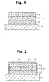
- FIG. 1 is a schematic sectional view of an organic electroluminescence device constituting a detection section of a sensor.
- the organic electroluminescence device 11 is formed on a substrate 12, and comprises an anode 13, an organic electroluminescence layer 14 and a cathode 15.
- a member provided on the light extraction side with respect to the organic electroluminescence layer 14, of the organic electroluminescence device 11 and the substrate 12, is transparent to light having a wavelength emitted outward from the organic electroluminescence device 11.
- the electroluminescence device 11 can be formed in the order of the cathode 15, the organic electroluminescence layer 14 and the anode 13 on the substrate 12.
- the anode 13 is an electrode injecting a positive hole into the organic electroluminescence layer 14 (positive hole transport layer in the configuration described later).
- a material for formation of the anode 13 may be any material imparting this nature to the anode 13, well known materials such as metals, alloys, electrically conductive compounds and mixtures thereof are generally selected, and the electrode is manufactured such that the work function of the surface (face contacting the organic electroluminescence layer 14) is 4eV or greater.
- Materials for formation of the anode 13 include, for example, the following materials:
- the anode 13 is provided on the light extraction side from the organic electroluminescence layer 14, generally, it is set so that the transmittance for extracted light is greater than 10%. If light in the visible range is extracted, ITO having a high transmittance in the visible range is suitably used.
- anode 13 is used as a reflecting electrode, a material having a capability of reflecting the light to be extracted outside is appropriately selected from the materials described above, and a metal, alloy or metal compounds are generally selected.
- the anode 13 may be formed by one type of the materials described above, or may be termed by mixing two or more types. Furthermore, it may be a multilayered structure composed of multiple layers of the same composition or different compositions.
- the auxiliary electrode is a metal such as copper, chromium, aluminum, titanium or an aluminum alloy or a layered product thereof partially provided in the anode 13.
- the anode 13 is formed by a well known thin film formation method such as a sputtering method, ion plating method, vacuum vapor deposition method, spin coating method or electron beam deposition method using the above mentioned materials.
- the surface may be subjected to UV ozone cleaning or plasma cleaning.
- the surface roughness should be controlled to be 20 nm or less as a mean-square value by a method for reducing the particle size or a method of polishing after film formation.
- the thickness of the anode 13 is selected to be generally about 5 nm to 1 ⁇ m, preferably about 10 nm to 1 ⁇ m, further preferably about 10 nm to 500 nm, especially preferably about 10 nm to 300 nm, desirably 10 nm to 200 nmdepending on the material that is used.
- the sheet electric resistance of the anode 13 is set to preferably several hundreds of ⁇ /square, more preferably about 5 to 50 ⁇ /square.
- the organic electroluminescence layer 14 may be a well known layer structure or layer of a well known material in a well known organic electroluminescence device, and can be manufactured by a well known manufacturing method.
- the organic electroluminescence layer 14 should realize at least the following capabilities, and may have a layered structure with each layer having any of the capabilities, or may have a single layer to realize the capabilities described below.
- layers maybe provided in the order of a positive hole transport layer, a light emission layer and an electron transport layer from the anode side to constitute the organic electroluminescence layer 14.
- the positive transport layer is a layer transporting the positive hole from the anode to the light emission layer.
- a material for formation of the positive hole transport layer may be selected from, for example, low molecular materials such as metal phthalocyanines and nonmetal phthalocyanines such as copper phthalocyanine and tetra (t-butyl) copper phthalocyanine, quinacridone compounds, aromatic amines such as 1,1-bis(4-di-p-triaminophenyl)cyclohexane, N,N'-diphenyl-N,N'-bis(3-methylphenyl)-1,1'-biphenyl-4,4'-d iamine and N,N'-di(1-naphtyl)-N,N'-diphenyl-1,1'-biphenyl-4,4'-diamine, polymer materials such as polythiophene and polyaniline, polythiophene oligomer materials, and other existing positive transport
- the light emission layer is a layer rebinding together the positive hole transported from the anode side and the electrode transported from the cathode side to enter into an excited state, and emitting light when returning to the ground state from the excited state.
- a material for the light emission layer a fluorescent material or phosphorescent material may be employed.
- a dopant fluorescent material or phosphorescent material may be incorporated in the host material.
- materials for formation of the light emission layer may be selected from, for example, low-molecular materials such as 9,10-diarylanthracene derivatives, pyrene derivatives, colonene derivatives, perylene derivatives, lubrene derivatives, 1,1,4,4-tetraphenylbutadiene, tris(8-quinolinolate) aluminum complexes, tris(4-methyl-8-quinolinolate) aluminum complexes, bis(8-quinolinolate) zinc complexes, tris(4-methyl-5-trifluoromethyl-8-quinolinolate) aluminum complexes, tris(4-methyl-5-cyano-8-quinolinolate)aluminum complexes, bis(2-methyl-5-trifluoromethyl-8-quinolinolate) [4-(4-cyanophenyl)phenolate] aluminum complexes, bis(2-methyl-5-cyano-8-quinolinolate) [4-(4-cyanophenyl)phenolate] aluminum complex
- the electron transport layer is a layer transporting an electron from the cathode to the light emission layer.
- Materials for formation of the electron transport layer include, for example, 2-(4-biphinylyl)-5-(4-t-butylphenyl)-1,3,4-oxadiazole, 2,5-bis(1-naphtyl)-1,3-4-oxadiazole and oxadiazole derivatives, bis(10-hydroxybenzo[h]quinolinolate) beryllium complexes and triazole compounds.
- the organic electroluminescence layer 14 can be provided with layers that can be employed in a well known organic electroluminescence layer, such as a buffer layer, a positive hole block layer, an electron injection layer and a positive hole injection layer, as a matter of course. These layers may be provided by a well known method using well known materials.
- the cathode 15 is an electrode injecting electrodes into the organic electroluminescence layer 14 (electron transport layer in the configuration described above), and metals and alloys, electrically conductive compounds and mixtures thereof having a work function, for example, less than 4.5 eV, generally equal to or less than 4.0 eV, typically equal to or less than 3.7 eV or less are employed as electrode materials for improving electron injection efficiency.
- the electrode materials described above include, for example, lithium, sodium, magnesium, gold, silver, copper, aluminum, indium, calcium, tin, ruthenium, titanium, manganese, chromium, yttrium, aluminum-calcium alloys, aluminum-lithium alloys, aluminum-magnesium alloys, magnesium-silver alloys, magnesium-indium alloys, lithium-indium alloys, sodium-potassium alloys, magnesium/copper mixtures and aluminum/aluminum oxide mixtures. Furthermore, a material capable of being employed as a material that is used in the anode may also be used.
- the cathode 15 is provided on the light extraction side from the light emission layer, generally, it is set so that the transmittance for extracted light is greater than 10% and for example, an electrode formedbystackingatransparent conductive oxide on a very thin magnesium-silver alloy, or the like, is employed. Furthermore, for preventing the light emission layer and the like from being damaged by plasma when the conductive oxide is sputtered, in the cathode, a buffer layer having copper phthalocyanine or he like should be provided between the cathode 15 and the organic luminescence layer 14.
- the cathode 15 is used as a light reflecting electrode, a material having a capability of reflecting the light to be extracted outside is appropriately selected from the materials described above, and a metal, alloy or metal compound is generally selected.
- the cathode 15 may be formed by one of the above materials alone, or may be formed by a plurality of materials. For example, if 5 to 10% of silver or copper is added to magnesium, oxidation of the cathode 15 can be prevented, and adhesion of the cathode 15 to the organic electroluminescence layer 14 is enhanced.
- the cathode 15 may be a multilayered structure composed of multiple layers of the same composition or different compositions.
- the structure described below can be used.
- the passivation film for example, silver or aluminum is suitably used.
- an oxide, fluoride or metal compound having a reduced work function is inserted into an interface area between the cathode 15 and the organic electroluminescence layer 14.
- lithium fluoride or lithium oxide is inserted into the interface area.
- the cathode 15 may be formed by a well known thin film formation method such as a vacuum vapor deposition method, sputtering method, ionization deposition method, ion plating method or electron beam deposition method.
- the thickness is set to generally about 5 nm to 1 ⁇ m, preferably about 5 nm to 1000 nm, especially preferably about 10 nm to 500 nm, desirably 50 nm to 200 nmdepending on the electrode material that is used.
- the sheet electric resistance of the cathode 15 is preferably set to several hundreds of ⁇ /square.
- the substrate 12 is generally a plate member supporting the organic electroluminescence device 11.
- the organic electroluminescence device 11 is generally fabricated as an organic EL device supported by the substrate 12 because each constituent layer is very thin.
- the substrate 12 is preferably has plane smoothness because it is a member on which the organic electroluminescence device 11 is stacked.
- the substrate 12 is placed on the light extraction side from the organic electroluminescence layer 14, it is transparent to extracted light.
- the substrate 12 a well known material may be used as long as it has the performance described above. Generally, glass substrates, silicon substrates, ceramic substrates such as quartz substrates and plastic substrates are selected. Furthermore, metal substrates and substrates with metal foils formed on supports are also used. Moreover, a substrate composed of a composite sheet having combined two or more of the same or different substrates may also be used.
- the organic electroluminescence device 11 has a terminal portion (not shown) of the anode 13 and a terminal portion (not shown) of the cathode 15 connected to a power source.
- a predetermined voltage is applied between both electrodes (anode 13 and cathode 15) from the power source, and the organic electroluminescence layer 14 has a positive hole injected thereinto from the anode 13 and an electrode injected thereinto from the cathode 15, recombines the positive hole and the electrode together to enter into an excited state, and emits light when returning to the ground state.
- gas in the ambient atmosphere can be detected.
- an area protected from gas in the ambient atmosphere, and an area 21a not protected from gas in the ambient atmosphere may be provided in the organic electroluminescence device 11.
- the above protected area should be protected by the substrate 12 and a protective member 20 comprising at least one of a passivation film and a sealing can. That is, the electroluminescence device should be designed to have an area contacting the substrate 12, an area protected by the protective member 20, and an area not protected from water and gas.
- the electroluminescence device is configured in this way, water or gas in the ambient atmosphere contacts and enters the organic electroluminescence device 11 mainly from the non-protected area 21a, and therefore the growth rate of a dark spot is reduced compared with an organic electroluminescence device that is not protected at all, and an organic electroluminescence device that is protected only by the substrate. The number of dark spots generated is also reduced. Thus, the above sensor can function for a longer time period.
- the area 21a not protected from gas may also be protected by a material permeable to the gas to be detected. If protection is provided in this way, the lifetime of the sensor can be prolonged. Furthermore, gas other than the detection object is hard to contact/enter the organic electroluminescence device 11, resulting in higher gas detection accuracy for the sensor.
- the passivation film is a protective layer (sealing layer) provided on the side opposite to the substrate for preventing the organic electroluminescence device 11 from contacting oxygen.
- Materials to be used for the passivation film may include, for example, organic polymer materials, inorganic materials and photo-curable resins, and the material to be used for the protective layer may be used alone, or in combination of two or more materials.
- the protective layer may be a single-layer structure or multilayered structure. The thickness of the passivation film is not limited as long as water and gas from outside can be blocked.
- organic polymer materials may include fluorine based resins such as chlorotrifluoroethylene polymers, dichlorodifluoroethylene polymers, and copolymers of chlorotrifluoroethylene polymersand dichlorodifluoroethylene polymers, acryl based resins such as polymethyl methacrylates and polyacrylates, epoxy resins, silicon resins, epoxysilicone resins, polystyrene resins, polyester resins, polycarbonate resins, polyamide resins, polyimide resins, polyamideimide resins, polyparaxylene resins, polyethylene resins and polyphenylene oxide resins.
- fluorine based resins such as chlorotrifluoroethylene polymers, dichlorodifluoroethylene polymers, and copolymers of chlorotrifluoroethylene polymersand dichlorodifluoroethylene polymers
- acryl based resins such as polymethyl methacrylates and polyacrylates
- epoxy resins silicon resins, epoxysilicone resins, poly
- Inorganic materials may include polysilazane, diamond thin films, amorphous silica, electrically resistant glass, metal oxides, metal nitrides, metal carbides and metal sulfates.
- the sealing can is a member provided composed of a sealing member such as a sealing plate or sealing container provided on the side opposite to the substrate 12 for blocking water and oxygen from outside.
- the sealing can may be placed only on the electrode side on the backside (opposite to the substrate 12), or may be situated to cover the entire organic electroluminescence device 11.
- the shape, size, thickness and the like of the sealing member are not specifically limited as long as it can seal the organic electroluminescence device 11 and block air from outside.
- materials to be used for the sealingmember glass, stainless steel, metals (aluminum, etc.), plastics (polychlorotrifluoroethylene, polyester, polycarbonate, etc.), ceramic and the like may be used.
- sealing agent adhesive
- the sealing member When the sealing member is placed in the organic electroluminescence device 11, a sealing agent (adhesive) may be used as appropriate. If the entire organic electroluminescence device 11 is coveredwith the sealingmember, sealing members may be heat-sealed without using the sealing agent.
- the sealing agent ultraviolet-curable resins, thermoset resins, two-pack curable resins and the like can be used.
- an area permanently protected from gas in the ambient atmosphere and an area 21b capable of switching between protected and non-protected states may be provided in the organic electroluminescence device 11.
- the above permanently protected area should be protected by the substrate 12 and the protective member 20 comprising at least one of a passivation film and a sealing can. That is, the permanently protected area in the organic electroluminescence device 11 is comprised of an area contacting the substrate 12 and an area protected by the protective member 20.
- the area 21b capable of switching between protected and non-protected states should be such that the organic electroluminescence device 11 is protected from gas by a cover member 22 in an initial state, and is in a non-protected state with part or all of the cover member 22 having been removed in a usage state.
- the cover member 22 is preferably constituted by a material protecting the organic electroluminescence device 11 from gas in the ambient atmosphere, e.g., a material for formation of the passivation film or a material for formation of the sealing can.
- the organic electroluminescence devise 11 In the initial state (non-usage state), the organic electroluminescence devise 11 is protected from gas in the ambient atmosphere by the substrate 12, the protective member 20 and the cover member 22.
- the cover member 22 is removed from the area 21b capable of switching between protected and non-protected states so that water and gas in the ambient atmosphere can contact the organic electroluminescence device 11 through the area 21b.
- the shape of the cover member 22 may be any shape as long as it can realize the above capabilities.
- the cover member 22 may have a shape such that part of the cover member 22 is accommodated in part of the protective member 20 that has been cut off, and may be bonded to the protective member 20 with an adhesive or the like in the initial state, and removed from the protective member 20 in the usage state.
- the cover member 22 may be a seal member, and may be bonded to the protective member 20 with an adhesive or the like in the initial state, and partially or wholly removed from the protective member 20 in the usage state.
- the organic electroluminescence device may be protected by at least the substrate and a protective layer (partially permeable layer) permeable to molecules having sizes equal to or smaller than a specified size. More preferably, the partially permeable layer is a passivation film and/or sealing can, and is permeable to molecules equal to or smaller than in size molecules of gas that are detected by the sensor.
- the partially permeable layer may cover the organic electroluminescence device 11, for example, with the passivation film and sealing can having a thickness allowing water and gas to permeate.
- the organic electroluminescence device 11 may be covered with a material permeable to at least water and gas to be detected by the sensor.
- the organic electroluminescence device may be protected by the substrate, and at least one of the passivation film and sealing can, with a through-hole bored in part of the passivation film or sealing can.
- a member such as a needle for boring a though-hole in part of the passivation filmor sealing can should be further provided in the sensor.
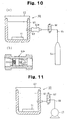
- the organic electroluminescence device 11 may be protected by the substrate 12 and a sealing can 23, and a through-hole making member constituted by a needle 24 for boring a though-hole in the sealing can, a press section 25 connected to the needle 24 and intended for pressing down the needle 24, and a cover 26 for holding the press section 25 at a predetermined position in the sealing can 23 may be provided outside the sealing can 23.
- the cover 26 is configured so that it can be partially or wholly removed from the sealing can 23, or so at least the water and gas to be detected by the sensor can pass through the cover 26.
- the organic electroluminescence device 11 is protected by the sealing can 23 and the substrate 12 in the initial state.
- the press section 25 is pressed from above the cover 26 toward the sealing can 23 side, and the needle 24 bores a through-hole in the sealing can 23.
- At least one of the electrodes should contain at least one element selected from alkali metals and alkali earth metals. This is because an electrode containing these metals is susceptible to degeneration such as oxidization and therefore tends to generate a dark spot and as a result, a very sensitive sensor can be provided.
- An inert gas may be enclosed in the passivation film or sealing can.
- An inert gas refers to a gas that does not react with the organic electroluminescence device 11, and rare gas such as helium and argon, or nitrogen gas may be employed. If this configuration is employed, a dark spot is difficult to be generated in the organic electroluminescence device 11 in the initial state, i.e., non-usage state, thus making it possible to prolong the lifetime of the sensor. Furthermore, in the initial state, storage of the gas sensor in a specified place is not required.
- a plurality of devices may be arranged in a matrix form rather than fully illuminating the organic electroluminescence device.
- the organic electroluminescence device may be used to display an image using the passive matrix control method or active matrix control method.
- the sensitivity of the sensor can be adjusted, and the sensor usable time period can be freely set.
- This detecting apparatus is characterized by comprising as a gas detection section the gas sensor described above, or a sensor with the above sensor altered as appropriate as described previously, and detecting gas in the ambient atmosphere using the gas detection method described previously.
- a first gas detecting apparatus will be described.
- a gas detecting apparatus is characterized by comprising as a gas detection section the gas sensor described above, or a sensor with the above sensor altered as appropriate as described previously, and detecting gas by a change in luminance when a predetermined voltage is continuously applied to the organic electroluminescence device. Furthermore, the concentration of gas maybe detected. Of course, both may be detected.
- the luminance of the organic electroluminescence device in which a dark spot is generated decreases in inverse proportion to the ratio of the total area of dark spots to the luminance area of the device, compared with a device in which no dark spots are generated.
- the gas detecting apparatus of the first embodiment it is comprised of the above gas sensor, a power source connected to electrodes of the sensor and applying a certain voltage to the sensor. A change in luminance is visually checked. Consequently, the user can see whether gas exists in the ambient atmosphere or not by merely checking brightness of the organic electroluminescence device 11. Furthermore, the concentration of water or gas can be determined.
- a display apparatus configured in the same manner as the above gas detecting apparatus except that the organic electroluminescence device is fully sealed should be fabricated and placed at a position so that the organic electroluminescence device in this apparatus can be compared with the organic electroluminescence device 11 in the above gas detecting apparatus.
- the display apparatus retaining brightness in the initial state can be visually compared with the detecting apparatus having a reduced luminance due to generation of a dark spot by gas in the ambient atmosphere, thus making it possible to determine more easily whether the luminance of the detecting apparatus has decreased or not.
- the luminance of the organic electroluminescence device decreases over time.
- the organic electroluminescence device of the display apparatus and the organic electroluminescence device of the detecting apparatus side-by-side as described above, whether the decrease in luminance of the organic electroluminescence device of the detecting apparatus results from a change with time or generation of a dark spot is easily determined.
- the above detecting apparatus may further comprise a luminance measuring apparatus (luminance detection section) 31 as a luminance measurement section measuring the luminance of the organic electroluminescence device 11, with a luminance detection and measurement section 31a measuring the luminance of the organic electroluminescence device 11. Consequently, a decrease in luminance of light emitted from the organic electroluminescence device 11 can be determined more accurately than a visual determination.
- a luminance measuring apparatus luminance detection section
- 31a luminance detection and measurement section 31a measuring the luminance of the organic electroluminescence device 11. Consequently, a decrease in luminance of light emitted from the organic electroluminescence device 11 can be determined more accurately than a visual determination.
- the organic electroluminescence device of the display apparatus and the organic electroluminescence device 11 of the detecting apparatus should be arranged side-by-side as described above, and the luminance of the device of the display apparatus should be measured.
- a determination section making the determination is preferably provided.
- an effect equivalent to that described above can be obtained by previously measuring light emission characteristics (result of change in characteristics associated with increasing time) of the organic electroluminescence device of the above display apparatus, and comparing the result of the measurement with the luminance of the organic electroluminescence device 11 of the above detecting apparatus.
- a storage section 32 storing the above light emission characteristics and a determination section 33 making the determination as described above are preferably provided as shown in FIG. 6.
- the determination section 33 is constituted by a microcomputer. Furthermore, in this configuration, it is not necessary to provide the above display apparatus.
- the gas detecting apparatus is characterized by measuring the area of dark spots in the organic electroluminescence device to detect gas. Furthermore, the concentration of gas or the like may be detected. Of course, both may be detected.
- This detecting apparatus is comprised of at least the organic electroluminescence device 11 and a power source connected to electrodes of the device. By checking any of the items described below, it can be determined that the water or gas to be detected is present in the ambient atmosphere.
- the concentration of gas in the ambient atmosphere can be determined.
- finding (C) described above there is a predetermined matching relation between the increasing rate of the total area of dark spots and the concentration of gas in the ambient atmosphere, and therefore a mathematical expression, matching table or the like indicating the relationship between the former and the latter can be created.
- the concentration of water or the like in the ambient atmosphere can be determined.
- an image analyzing apparatus (measurement section) 34 image-analyzing the display area of the organic electroluminescence device 11 should be provided as shown in FIG. 7.
- the image analyzing apparatus 34 comprises at least an imaging section 35 comprised of a CCD or the like forming an image of the display area of the organic electroluminescence device 11, and an area calculation section 36 making a determination based on dark spots in the display area from the image formed by the imaging section 35 and calculating the area of the dark spots.
- the area calculation section 36 is constituted by a microcomputer.
- the gas detecting apparatus of the third embodiment is characterized by detecting gas by a change in voltage value required for illuminating the organic electroluminescence device at a predetermined luminance. Furthermore, the concentration of gas may be detected. Of course, both may be detected.
- the luminance of the organic electroluminescence device 11 decreases if a dark spot is generated.
- the luminance of an area free from a dark spot must be increased and for this purpose, the magnitude of a voltage to be applied to the device must be increased.
- the detecting apparatus of the third embodiment detects the presence/absence of gas in the ambient atmosphere, and the concentration of gas.
- the third detecting apparatus comprises at least a luminance measuring apparatus (luminance measurement section) 51, a determination apparatus (determination section) 52 and a power source section 53
- the luminance measuring apparatus 51 measures the luminance of the organic electroluminescence device 11.
- the determination apparatus 52 determines the magnitude of a voltage to be applied to the organic electroluminescence device 11 based on the result of measurement by the luminance measuring apparatus 51.
- the power source section 53 applies a voltage based on the result of determination by the determination apparatus 52 to the organic electroluminescence device 11.
- light emission characteristics (characteristics in change with time) of the organic electroluminescence device fully protected from water and gas are preferably considered before detection is performed as in the case of the gas detecting apparatus of the first embodiment.
- the gas detecting apparatus is characterized by detecting gas based on a change in voltage value in the organic electroluminescence device 11 when a predetermined voltage is applied to the device.
- the detecting apparatus detects the presence/absence of gas and the concentration thereof in the ambient atmosphere by measuring generation of dark spots, and the increasing rate of the total area of dark spots taking advantage of the change in voltage characteristics due to generation of dark spots.
- a detecting apparatus should only comprise at least a power source section passing a certain current through the organic electroluminescence device 11, and a voltage measurement section (measurement section) measuring a voltage in the organic electroluminescence device 11.
- the voltage arises, it can be determined that a dark spot is generated, and therefore it can be determined that water or gas exists in the ambient atmosphere.
- the increasing rate of the total area of dark spots can be calculated from the degree of drop in voltage to calculate the concentration of water or gas in the ambient atmosphere.
- the detecting apparatus should further comprise a determination apparatus (determination section) determining whether the voltage value in the organic electroluminescence device 11 is a predetermined value or not, and make the determination apparatus perform the above calculation.
- the organic electroluminescence device has characteristics such that if a certain current is passed through the device, the voltage in the device increases, more accurate detection can be performed if such characteristics (voltage characteristics and current characteristics associated with increasing time) are considered before the above calculation is performed.
- a detecting apparatus is not required to measure a luminance and determine the size and number of dark spots, and therefore the organic electroluminescence device 11 configured to emit no light to the outside may also be employed.
- an anode and a cathode may be each constituted by a metal electrode.
- a very high degree of freedom can be obtained for the material and method for formation of the organic electroluminescence device 11 and the layer structure of the device.
- a gas detecting apparatus can be changed into an apparatus for detecting a specific type of gas, and an apparatus for detecting various types of gases, by appropriately designing and altering the sensor as described previously.
- the detecting apparatus can be changed into an apparatus measuring for humidity in the ambient atmosphere, or an apparatus measuring the degree of vacuum in the ambient atmosphere, or an apparatus for measuring oxygen in the ambient atmosphere.
- a gas detecting apparatus can be changed into a new detecting apparatus by changing only the organic electroluminescence device 11.
- the presence of gas can be detected visually, the concentration thereof can be detected, and more accurate detection can be performed if it is combined with the above measuring apparatuses and the like.
- a method for storing a gas sensor according to the first embodiment is characterized in that at least the organic electroluminescence device 11 is placed under an inert gas for the device or placed under vacuum until it is used.
- parts other than the organic electroluminescence device 11 may be stored under the environment described above as a matter of course.
- a storage vessel for a gas sensor according to this embodiment is characterized by having a structure capable of using the technical idea of the above method for storing the gas sensor.
- the above storage vessel 60 has a housing 61 as a storage section for storing at least the organic electroluminescence device 11, and the housing 61 comprises a cover 62 as a switching member for switching between isolation from and exposure to the exterior of the storage vessel 60. That is, the storage vessel 60 can contain at least the organic electroluminescence device 11 within the housing 61, and isolate the interior of the housing 61 from the ambient atmosphere by the cover 62.
- a storage vessel according to the first embodiment is not limited to the configuration shown in FIG. 9, and can employ any housing irrespective of its shape, material, size, etc. as long as the above technical idea, i.e., action can be obtained.
- parts other than the organic electroluminescence device 11 may also be stored under the housing 61.
- this storage vessel may have any of the following configurations (I) to (IV).
- connection section comprises a mechanism, such as a valve or shutter, which can be connected to a suction device such as an aspirator or suction pump provided outside, and allows the interior of the storage section to communicate with the exterior (suction device) when being suctioned by the suction device, and cuts off (isolates) the interior of the storage vessel from the exterior when not being suctioned by the suction device in configuration (II).
- a suction device such as an aspirator or suction pump provided outside
- the electroluminescence device can be stored under vacuum.
- the organic electroluminescence device 11 may not be protected with the passivation film or sealing can, or may be only provided with a protective layer using a material having poor water and gas barrier properties.
- a storage vessel of the gas detecting apparatus according to this embodiment will now be described along with the gas detection method according to this embodiment.
- a method for storing the gas detecting apparatus according to this embodiment is characterized in that at least the electroluminescence device is placed under inert gas for the device or under vacuum until it is used.
- parts other than the organic electroluminescence device 11 may be stored under the above environment as a matter of course.
- a storage vessel for the gas detecting apparatus is characterized by having a structure capable of using the technical idea of the method for storing the above gas detecting apparatus.
- the above storage vessel is characterized by comprising a storage section for storing at least the electroluminescence device, the storage section comprising a section of isolation from exposure to the exterior of the storage vessel. That is, the storage vessel can store at least the electroluminescence device in the storage section, and isolate the interior of the storage section from the ambient atmosphere.
- a storage vessel according to this embodiment is not limited to the configuration described above, but may employ any housing irrespective of its shape, material, size, etc., as long as the above technical idea, i.e., action can be obtained.
- parts other than the organic electroluminescence device 11 may be stored in the storage section.
- this storage vessel may have any of the following configurations (V) to (VIII).
- This configuration is equivalent to the configuration (IV) described above, and allows at least the electroluminescence device to be stored under vacuum.
- a method and device for detecting gas in the ambient atmosphere and/or the concentration of gas in the ambient atmosphere by providing an electroluminescence device is performed based on the presence of a dark spot in the electroluminescence device, which is caused by exposure of the electroluminescence device to gas in the ambient atmosphere.
Landscapes
- Physics & Mathematics (AREA)
- Health & Medical Sciences (AREA)
- Chemical & Material Sciences (AREA)
- Pathology (AREA)
- General Physics & Mathematics (AREA)
- Immunology (AREA)
- Life Sciences & Earth Sciences (AREA)
- Analytical Chemistry (AREA)
- Biochemistry (AREA)
- General Health & Medical Sciences (AREA)
- Plasma & Fusion (AREA)
- Chemical Kinetics & Catalysis (AREA)
- Engineering & Computer Science (AREA)
- Nuclear Medicine, Radiotherapy & Molecular Imaging (AREA)
- Optics & Photonics (AREA)
- Electroluminescent Light Sources (AREA)
- Investigating Or Analysing Materials By The Use Of Chemical Reactions (AREA)
- Investigating, Analyzing Materials By Fluorescence Or Luminescence (AREA)
Applications Claiming Priority (2)
| Application Number | Priority Date | Filing Date | Title |
|---|---|---|---|
| JP2003279915 | 2003-07-25 | ||
| JP2003279915A JP2005043303A (ja) | 2003-07-25 | 2003-07-25 | 水分・ガス検出方法、水分・ガスセンサ、当該センサを用いた水分・ガス検出装置、当該水分・ガスセンサ及び前記水分・ガス検出装置の保管方法並びに保管器 |
Publications (2)
| Publication Number | Publication Date |
|---|---|
| EP1500922A2 true EP1500922A2 (de) | 2005-01-26 |
| EP1500922A3 EP1500922A3 (de) | 2005-04-13 |
Family
ID=33487724
Family Applications (1)
| Application Number | Title | Priority Date | Filing Date |
|---|---|---|---|
| EP04017327A Withdrawn EP1500922A3 (de) | 2003-07-25 | 2004-07-22 | Elektrolumineszenzgassensor und verfahren zum gasnachweis |
Country Status (6)
| Country | Link |
|---|---|
| US (1) | US20050019947A1 (de) |
| EP (1) | EP1500922A3 (de) |
| JP (1) | JP2005043303A (de) |
| KR (1) | KR20050012684A (de) |
| CN (1) | CN1576825A (de) |
| TW (1) | TWI273236B (de) |
Cited By (2)
| Publication number | Priority date | Publication date | Assignee | Title |
|---|---|---|---|---|
| DE102006029721B4 (de) * | 2005-07-20 | 2008-02-07 | Lg. Philips Lcd Co., Ltd. | Verfahren zur Herstellung eines 9,10-Diarylanthracens |
| DE102006029417B4 (de) * | 2005-07-20 | 2008-02-14 | Lg. Philips Lcd Co., Ltd. | Verfahren zur Herstellung eines 9,10 Diarylanthracens |
Families Citing this family (22)
| Publication number | Priority date | Publication date | Assignee | Title |
|---|---|---|---|---|
| JP4827589B2 (ja) * | 2006-04-05 | 2011-11-30 | 株式会社半導体エネルギー研究所 | 湿度検出装置 |
| GB2438423A (en) * | 2006-05-24 | 2007-11-28 | Univ Graz Tech | Optical sensor for detecting an analyte |
| US7969569B2 (en) * | 2006-10-16 | 2011-06-28 | National Institute Of Advanced Industrial Science And Technology | Method for detecting trace substance using organic electroluminescent device |
| DE102006055797B4 (de) * | 2006-11-27 | 2024-01-11 | Robert Bosch Gmbh | Sensorelement für einen Gasssensor zur Bestimmung einer physikalischen Eigenschaft eines Messgases |
| US8907802B2 (en) | 2012-04-29 | 2014-12-09 | Valor Fire Safety, Llc | Smoke detector with external sampling volume and ambient light rejection |
| US9140646B2 (en) | 2012-04-29 | 2015-09-22 | Valor Fire Safety, Llc | Smoke detector with external sampling volume using two different wavelengths and ambient light detection for measurement correction |
| US8947244B2 (en) | 2012-04-29 | 2015-02-03 | Valor Fire Safety, Llc | Smoke detector utilizing broadband light, external sampling volume, and internally reflected light |
| KR20150000227A (ko) * | 2013-06-24 | 2015-01-02 | 삼성디스플레이 주식회사 | 유기 발광 장치 |
| CN104280442B (zh) | 2013-07-12 | 2018-04-27 | 株式会社杰士汤浅国际 | 伽伐尼电池式氧传感器 |
| JP6407295B2 (ja) | 2013-10-30 | 2018-10-17 | ヴァラー ファイヤー セーフティー, エルエルシー | 外部サンプリング体積および周囲光拒絶を有する煙検出器 |
| TW201525442A (zh) * | 2013-12-27 | 2015-07-01 | 菱生精密工業股份有限公司 | 微型封裝結構之氣體感知器及其製造方法 |
| CN105489969A (zh) * | 2015-12-02 | 2016-04-13 | 黎海纤 | 一种空气电池组及其制作方法 |
| CN105352940A (zh) * | 2015-12-02 | 2016-02-24 | 蔡权 | 一种新型继电保护器及其制作方法 |
| CN105352938A (zh) * | 2015-12-02 | 2016-02-24 | 肖锐 | 一种具有气体检测功能的高压电源及其制作方法 |
| CN105352937A (zh) * | 2015-12-02 | 2016-02-24 | 钟林超 | 一种新型机器人及其制作方法 |
| CN105270671A (zh) * | 2015-12-02 | 2016-01-27 | 杨炳 | 一种真空包装机及其制作方法 |
| CN105449467A (zh) * | 2015-12-02 | 2016-03-30 | 杨超坤 | 一种具有气体报警功能的安全插座及其制作方法 |
| CN105352941A (zh) * | 2015-12-02 | 2016-02-24 | 陈杨珑 | 一种生物质反应炉及其制作方法 |
| EP3879561A1 (de) * | 2020-03-10 | 2021-09-15 | Sensirion AG | Verfahren zur herstellung einer elektronischen vorrichtung |
| JP2021192017A (ja) * | 2020-06-05 | 2021-12-16 | パナソニックIpマネジメント株式会社 | ガスセンサ素子及びそれを用いたガス検出装置 |
| DE102021119709A1 (de) | 2021-07-29 | 2023-02-02 | OSRAM Opto Semiconductors Gesellschaft mit beschränkter Haftung | Anordnung, verfahren zur montage eines optoelektronischen bauteils und optoelektronisches bauteil |
| CN115078400A (zh) * | 2022-06-10 | 2022-09-20 | 江苏富乐华功率半导体研究院有限公司 | 一种陶瓷基板缺陷检测装置及缺陷检测方法 |
Family Cites Families (13)
| Publication number | Priority date | Publication date | Assignee | Title |
|---|---|---|---|---|
| JPS5852473A (ja) * | 1981-09-21 | 1983-03-28 | Mitsubishi Heavy Ind Ltd | 金属材料の表面処理法 |
| JPH0742583B2 (ja) * | 1986-05-23 | 1995-05-10 | 日本電信電話株式会社 | 薄膜形成装置 |
| FR2714454B1 (fr) * | 1993-12-28 | 1996-02-09 | Etat Francais Labo Cl Ponts Ch | Dispositif de signalisation visible sur 360 degré logeant de manière étanche une source lumineuse. |
| JPH0850096A (ja) * | 1994-08-04 | 1996-02-20 | Toyota Central Res & Dev Lab Inc | 電界発光素子を利用したガス検出装置 |
| JP2715942B2 (ja) * | 1994-11-29 | 1998-02-18 | 日本電気株式会社 | 波長変換装置 |
| CA2199096C (en) * | 1996-03-05 | 2001-01-23 | Soichiro Kawakami | Process and apparatus for recovering components of sealed type battery |
| US5994835A (en) * | 1997-01-13 | 1999-11-30 | Xerox Corporation | Thin film organic light emitting diode with edge emitter waveguide and electron injection layer |
| GB9712483D0 (en) * | 1997-06-17 | 1997-08-20 | Kathirgamanathan Poopathy | Fabrication of light emitting devices from chelates of transition metals, lanthanides and actinides |
| JPH11329719A (ja) * | 1998-04-08 | 1999-11-30 | Lg Electronics Inc | 有機電界発光素子 |
| US6160267A (en) * | 1999-01-05 | 2000-12-12 | Regents Of The University Of Minnesota | Vapochromic led |
| JP2003086355A (ja) * | 2001-09-05 | 2003-03-20 | Kiko Kenji Kagi Kofun Yugenkoshi | 有機el素子の封止構造並びに封止方法及び封止装置 |
| US7214543B2 (en) * | 2001-10-12 | 2007-05-08 | University Of Florida Research Foundation, Inc. | Method and apparatus for sensing nitroaromatics |
| JP3868280B2 (ja) * | 2001-12-04 | 2007-01-17 | 株式会社美和製作所 | 有機電界発光素子の製造装置 |
-
2003
- 2003-07-25 JP JP2003279915A patent/JP2005043303A/ja active Pending
-
2004
- 2004-07-22 TW TW093121840A patent/TWI273236B/zh not_active IP Right Cessation
- 2004-07-22 EP EP04017327A patent/EP1500922A3/de not_active Withdrawn
- 2004-07-23 US US10/897,831 patent/US20050019947A1/en not_active Abandoned
- 2004-07-23 KR KR1020040057815A patent/KR20050012684A/ko not_active Ceased
- 2004-07-23 CN CNA2004100684587A patent/CN1576825A/zh active Pending
Cited By (4)
| Publication number | Priority date | Publication date | Assignee | Title |
|---|---|---|---|---|
| DE102006029721B4 (de) * | 2005-07-20 | 2008-02-07 | Lg. Philips Lcd Co., Ltd. | Verfahren zur Herstellung eines 9,10-Diarylanthracens |
| DE102006029417B4 (de) * | 2005-07-20 | 2008-02-14 | Lg. Philips Lcd Co., Ltd. | Verfahren zur Herstellung eines 9,10 Diarylanthracens |
| US7622619B2 (en) | 2005-07-20 | 2009-11-24 | Lg Display Co., Ltd. | Synthesis process |
| US8766023B2 (en) | 2005-07-20 | 2014-07-01 | Lg Display Co., Ltd. | Synthesis process |
Also Published As
| Publication number | Publication date |
|---|---|
| JP2005043303A (ja) | 2005-02-17 |
| TWI273236B (en) | 2007-02-11 |
| US20050019947A1 (en) | 2005-01-27 |
| CN1576825A (zh) | 2005-02-09 |
| TW200508603A (en) | 2005-03-01 |
| EP1500922A3 (de) | 2005-04-13 |
| KR20050012684A (ko) | 2005-02-02 |
Similar Documents
| Publication | Publication Date | Title |
|---|---|---|
| EP1500922A2 (de) | Elektrolumineszenzgassensor und verfahren zum gasnachweis | |
| US7250721B2 (en) | Organic EL element and organic EL display panel | |
| US6611098B2 (en) | Hermetic encapsulation package and method of fabrication thereof | |
| US7855506B2 (en) | Electric field light emitting element | |
| US10418575B2 (en) | OLED with mixed layer between the hole transport and emission layers | |
| JP2008153004A (ja) | 有機エレクトロルミネッセンス素子 | |
| JP2001338755A (ja) | 有機el素子およびその製造方法 | |
| US20100044736A1 (en) | Semiconductor apparatus and method of manufacturing same | |
| CN100448060C (zh) | 有机电致发光元件以及有机电致发光显示器 | |
| JPH04328295A (ja) | 有機エレクトロルミネッセンス素子 | |
| US7233105B2 (en) | Organic electroluminescent display device having plural carrier transportation layers | |
| JP2003297554A (ja) | 発光素子およびこれを用いた表示装置並びに照明装置 | |
| JP2005174701A (ja) | 電界発光デバイス | |
| JPH04328294A (ja) | 有機エレクトロルミネッセンス素子 | |
| KR100790672B1 (ko) | 유기 일렉트로루미네센스 소자 및 유기 일렉트로루미네센스디스플레이 | |
| KR100699966B1 (ko) | 유기 일렉트로루미네선스 소자 및 유기 일렉트로루미네선스디스플레이 | |
| JP2001110569A (ja) | 有機発光素子および画像表示装置 | |
| JPWO2005122702A1 (ja) | 有機エレクトロルミネセンス素子、その検査装置及び検査方法 | |
| JP2010114312A (ja) | 有機エレクトロルミネッセンス素子 | |
| JP2003297550A (ja) | 発光素子およびこれを用いた表示装置並びに照明装置 | |
| JP2009276721A (ja) | 電気光学装置及びその検査方法並びに電子機器 | |
| JP3693033B2 (ja) | 発光素子およびその製造方法 | |
| JPH118074A (ja) | 有機エレクトロルミネッセンス素子 | |
| CN101176384A (zh) | 有机电致发光元件 | |
| KR100581640B1 (ko) | 유기 전계발광 소자 |
Legal Events
| Date | Code | Title | Description |
|---|---|---|---|
| PUAI | Public reference made under article 153(3) epc to a published international application that has entered the european phase |
Free format text: ORIGINAL CODE: 0009012 |
|
| 17P | Request for examination filed |
Effective date: 20040722 |
|
| AK | Designated contracting states |
Kind code of ref document: A2 Designated state(s): AT BE BG CH CY CZ DE DK EE ES FI FR GB GR HU IE IT LI LU MC NL PL PT RO SE SI SK TR |
|
| AX | Request for extension of the european patent |
Extension state: AL HR LT LV MK |
|
| PUAL | Search report despatched |
Free format text: ORIGINAL CODE: 0009013 |
|
| RTI1 | Title (correction) |
Free format text: ELECTROLUMINESCENT GAS SENSOR AND GAS DETECTION METHOD |
|
| AK | Designated contracting states |
Kind code of ref document: A3 Designated state(s): AT BE BG CH CY CZ DE DK EE ES FI FR GB GR HU IE IT LI LU MC NL PL PT RO SE SI SK TR |
|
| AX | Request for extension of the european patent |
Extension state: AL HR LT LV MK |
|
| AKX | Designation fees paid |
Designated state(s): DE FI GB NL |
|
| 17Q | First examination report despatched |
Effective date: 20061122 |
|
| STAA | Information on the status of an ep patent application or granted ep patent |
Free format text: STATUS: THE APPLICATION IS DEEMED TO BE WITHDRAWN |
|
| 18D | Application deemed to be withdrawn |
Effective date: 20070403 |