EP1500904A1 - Procede et instrument de mesure de la forme de coupe du manchon de verre d'un tube electrique soude - Google Patents
Procede et instrument de mesure de la forme de coupe du manchon de verre d'un tube electrique soude Download PDFInfo
- Publication number
- EP1500904A1 EP1500904A1 EP03719173A EP03719173A EP1500904A1 EP 1500904 A1 EP1500904 A1 EP 1500904A1 EP 03719173 A EP03719173 A EP 03719173A EP 03719173 A EP03719173 A EP 03719173A EP 1500904 A1 EP1500904 A1 EP 1500904A1
- Authority
- EP
- European Patent Office
- Prior art keywords
- bead
- image
- pipe
- electric resistance
- shape
- Prior art date
- Legal status (The legal status is an assumption and is not a legal conclusion. Google has not performed a legal analysis and makes no representation as to the accuracy of the status listed.)
- Granted
Links
Images


Classifications
-
- B—PERFORMING OPERATIONS; TRANSPORTING
- B23—MACHINE TOOLS; METAL-WORKING NOT OTHERWISE PROVIDED FOR
- B23K—SOLDERING OR UNSOLDERING; WELDING; CLADDING OR PLATING BY SOLDERING OR WELDING; CUTTING BY APPLYING HEAT LOCALLY, e.g. FLAME CUTTING; WORKING BY LASER BEAM
- B23K11/00—Resistance welding; Severing by resistance heating
- B23K11/24—Electric supply or control circuits therefor
- B23K11/25—Monitoring devices
- B23K11/252—Monitoring devices using digital means
-
- B—PERFORMING OPERATIONS; TRANSPORTING
- B21—MECHANICAL METAL-WORKING WITHOUT ESSENTIALLY REMOVING MATERIAL; PUNCHING METAL
- B21C—MANUFACTURE OF METAL SHEETS, WIRE, RODS, TUBES OR PROFILES, OTHERWISE THAN BY ROLLING; AUXILIARY OPERATIONS USED IN CONNECTION WITH METAL-WORKING WITHOUT ESSENTIALLY REMOVING MATERIAL
- B21C37/00—Manufacture of metal sheets, bars, wire, tubes or like semi-manufactured products, not otherwise provided for; Manufacture of tubes of special shape
- B21C37/06—Manufacture of metal sheets, bars, wire, tubes or like semi-manufactured products, not otherwise provided for; Manufacture of tubes of special shape of tubes or metal hoses; Combined procedures for making tubes, e.g. for making multi-wall tubes
- B21C37/08—Making tubes with welded or soldered seams
- B21C37/0807—Tube treating or manipulating combined with, or specially adapted for use in connection with tube making machines, e.g. drawing-off devices, cutting-off
- B21C37/0811—Tube treating or manipulating combined with, or specially adapted for use in connection with tube making machines, e.g. drawing-off devices, cutting-off removing or treating the weld bead
-
- B—PERFORMING OPERATIONS; TRANSPORTING
- B21—MECHANICAL METAL-WORKING WITHOUT ESSENTIALLY REMOVING MATERIAL; PUNCHING METAL
- B21C—MANUFACTURE OF METAL SHEETS, WIRE, RODS, TUBES OR PROFILES, OTHERWISE THAN BY ROLLING; AUXILIARY OPERATIONS USED IN CONNECTION WITH METAL-WORKING WITHOUT ESSENTIALLY REMOVING MATERIAL
- B21C51/00—Measuring, gauging, indicating, counting, or marking devices specially adapted for use in the production or manipulation of material in accordance with subclasses B21B - B21F
-
- G—PHYSICS
- G01—MEASURING; TESTING
- G01B—MEASURING LENGTH, THICKNESS OR SIMILAR LINEAR DIMENSIONS; MEASURING ANGLES; MEASURING AREAS; MEASURING IRREGULARITIES OF SURFACES OR CONTOURS
- G01B11/00—Measuring arrangements characterised by the use of optical techniques
- G01B11/24—Measuring arrangements characterised by the use of optical techniques for measuring contours or curvatures
Definitions
- the present invention relates to a method and device for measuring welded bead cutting shapes in electric resistance welded pipes, including the position of the bead.
- electric resistance welded pipes such as electric resistance steel pipes
- electric resistance steel pipes are manufactured by continuously forming steel plates or steel coils into a tubular form, and continuously performing butt welding both sides of the steel coil in the longitudinal direction by means such as high-frequency induction heat-pressure welding or resistance heat-pressure welding.
- a raised portion called a "bead” is formed at the weld portion of the electric resistance welded pipe due to the butt welding, on the inside of the pipe and the outside of the pipe.
- the bead is continuously cut in the longitudinal direction of the steel pipe by a cutting tool on the production line further downstream from the welder.
- the shape of the surface of the pipe after the bead portion has been cut off (hereafter referred to as "bead cutting shape”) preferably becomes one with the outline shape of the pipe other than the weld, such that where the bead was cannot be distinguished, ideally.
- the cutting tool tip must be held at an appropriate position on the surface of the electric resistance welded pipe.
- the bead cutting portion cannot be directly observed during manufacturing, due to the configuration of the production line. Accordingly, the end portion of the pipe is observed at the process where the pipe is cut at the end position of the line. Alternatively, the line is stopped to cut out a sample of the bead position of the pipe by gas cutting, and the inner face is observed.
- the observation position is several tens of meters downstream from the cutting position, so there has been a problem in that in the event that an abnormality occurs in the cutting, the defective pipe becomes longer until detected, resulting in decrease in yield.
- the cutting tool seizes due to friction heat in the event that the line is stopped, so the cutting tool must be retracted.
- a bead cutting shape measurement method using the optical cutting method has been proposed.
- Examples of the optical cutting method are disclosed in Japanese Unexamined Patent Application Publication No. 57-108705 and Japanese Examined Patent Application Publication No. 60-1138.
- slit light 121 from a light source 120 is cast on a measuring object (electric resistance welded pipe 110), and this is observed from a different angle with a camera 130, thereby observing a slit image (optical cutting image) deformed following the surface shape of the measuring object 110.
- the shape of the object can be calculated from this optical cutting image and the geometric position of the observation optical system. This is advantageous in that the observation optical system is simple, that the measurement sensitivity can be widely changed according to the geometric placement of the observation optical system, and so forth.
- the region outside of the irradiation region of the slit light is called "background texture".
- Japanese Unexamined Patent Application Publication No. 52-96049 proposes a bead shape observation method wherein an uncut weld bead portion is observed with the optical cutting method, and marks corresponding to an enlargement ratio determined by optical placement on a display monitor 140.
- An example of a determination method for automatic measurement is the technique disclosed in Japanese Patent No. 2618303, for example. According to this, a method is proposed wherein a picture is taken of the steel pipe bead cutting portion using an optical cutting image from slit light and an ITV camera at the time of measuring the shape following cutting the welding bead of the electric resistance welded pipe, and as shown in Fig.
- the cross-sectional shape is calculated by performing thinning processing (taking a region wherein one pixel is connected in one direction as a thin line) on the cross-sectional shape picture, the cut portion and uncut portion are distinguished by the luminance of the cross-sectional shape, the value for the center of the distinguished cut portion and the value at the right edge of the cut portion and the value at the left edge of the cut portion are obtained, and the cutting depth, and amount of cutting inclination are calculated based on these three calculated values.
- the specific method for thinning processing only involves performing computation for directly substituting luminance to Y-axial coordinates, such as plotting the maximum luminance in a direction parallel to the pipe axis (Y-axial direction) obtained from the optical cutting image onto the coordinates on an X axis extending in the circumferential direction of the pipe (this is equivalent to the width direction for material steel plates and steel coils, and accordingly with hereafter be referred to as the width direction), so there is the problem in that there are cases wherein an accurate cross-sectional shape cannot be obtained.
- the luminance of the optical cutting image of the bead cutting portion is not necessarily around the same degree in the width direction.
- Fig. 14 there are cases such as in Fig. 14 wherein almost all of the slit light of the cut portion exhibits specular reflection (reflection in the opposite direction to the incident direction at the same angle as the incident angle), with the luminance thereof being one-tenth or less than that of the uncut portion. This is due to the fact that in the event that the incident angle and the reception angle differ, such specular reflection light actually appears to have less luminance.
- the present invention has been made to solve the problems such as described above, and accordingly, it is an object thereof to provide a method and device for precisely measuring the bead cutting shape of electric resistance welded pipe without being affected by the difference in luminance level between the cut portion and uncut portion in optical cutting images.
- Japanese Unexamined Patent Application Publication No. 57-208404 proposes a method wherein an optical cutting image is searched vertically from top to bottom and an optical cutting line is extracted only from within a section wherein a portion greater than a predetermined setting value first occurs, and subsequent extraction of optical cutting lines is terminated at the one scanning line, thereby preventing erroneously detecting abnormal reflections at portions of the optical cutting line on the object other than the slit luminescent line position.
- Japanese Unexamined Patent Application Publication No. 2-35306 proposes a shape detecting method wherein the entire region of the acquired optical cutting image is scanned in the direction crossing the optical cutting line, and in the event that there is a peak value due to the noise image on the scanning line, an optical cutting search range is set based on the optical cutting line position detected on the same scanning line over the entire screen, thereby ignoring noise.
- Japanese Unexamined Patent Application Publication No. 4-240508 proposes a three-dimensional shape recognition device for calculating coordinates of an object of measurement based on an optical cutting image, and judging the image to be an unreal image in the event that the shape thereof exists in a needle-like shape separated from surrounding images, thereby ignoring that data and recognizing the shape.
- a fixed threshold V1 is used for recognizing the only optical cutting extraction section, so application thereof to measuring bead cutting shapes wherein the luminance of the optical cutting line of the acquired optical cutting image changes greatly between the cut portion and uncut portion is impossible, as already described.
- Japanese Unexamined Patent Application Publication No. 2-35306 assumes that parts having raised shapes with a generally uniform size in the longitudinal direction are arrayed in the direction of the slit light at equal intervals, as with soldered portions of electronic parts, and generation of noise is explained as being secondary light due to reflected slit light off of a neighboring part, so this is clearly inapplicable to the problems of the present invention since a similar noise generation state is not generated at the cut portion of an electric resistance welded pipe.
- the present invention has been made to solve the above-described problems, and accordingly it is an object thereof to provide a measurement method and measurement device which can readily recognize image processing abnormality portions due to deterioration in the SN ratio in three-dimensional shape measurement by the optical cutting method as being uneven portions due to cutting.
- Patent Document 1 proposes a method for detecting deviation of the outer face weld portions of the running pipe using contact-type rollers.
- Patent Document 2 proposes a center position detection method for the welding bead wherein a detecting head comprising a magnetic core, performing uniform circular motion on a concentric axis within a transmission coil and reception coil disposed in a concentric cylindrical fashion, is erected above the welding bead and brought into close proximity, and at the time of the magnetic core passing over the welding bead, passage timing is detected twice per rotation of the magnetic core based on the change in impedance of the reception coil, with the time passing between these passage timings being computed and compared, thereby detecting the center position of the welding bead.
- Patent Document 3 proposes a method wherein a plurality of eddy current sensors are disposed in a form generally extending in one direction, and scanning the object of detection by sequentially switching the roles of the eddy current sensors between magnetization, induced-magnetization, and detection, thereby detecting the bead position from the detection waveform.
- Patent Document 6 proposes a bead shape automatic measuring device as a common welding bead position and shape automatic measurement technique, wherein an image is taken of the welding bead from above and from the side, analog image information from the image-taking unit is converted into grayscale level digital information, and the width and height and the like of the welding bead is detected based on the digital image information.
- the height of the bead must be approximately constant in the longitudinal direction with the irregularities in height thereof being relatively steep, so in the event that the irregularities in height of the bead is constantly smooth, in the event that the bead height is low, or in the event that the bead height is not constant in the longitudinal direction, accurate detection cannot be made.
- Patent Document 3 wherein magnetization, induced-magnetization, and detection coils are disposed generally in one direction, readily responds to foreign material adhering to the surface of the pipe and irregularities and so forth in the height of the surface of the pipe besides the bead, so it is difficult to avoid erroneous detection, and also, in the event of dealing with various sizes such as with electric resistance welded pipes, multiple detecting heads must be prepared to handle the difference in shape thereof, which increases manufacturing costs.
- the optical methods such as disclosed in Patent Document 4 and Patent Document 5 allow non-contact detection, and are advantageous in that not only bead position detection but also bead shape evaluation can be made with the same device configuration.
- the present invention has been made to solve the problems of the conventional art described above, and it is an object thereof to provide a method and device for accurately detecting the bead shape from the shape data of electric resistance welded pipes with the so-called optical cutting method detected by slit light or point light scanning, without effects of luminance or profile data noise.
- Patent Document 7 a metal flow angle measurement method for electric resistance welded pipes has been proposed, wherein slit light is irradiated before bead cutting on a base pipe which is moving and the optical cutting profile obtained thereby is optically received as image, the width and height of the bead at the welded portion is detected from the obtained optical cutting profile reception signals, and the metal flow angle of the welded portion is computed based on the detection values of the width and height of the bead thus obtained.
- Patent Document 8 proposes a metal flow angle measurement method for the welded portion of electric resistance welded pipes, wherein slit light is irradiated before bead cutting on a base pipe which is moving and optical cutting profiles each obtained thereby are optically received as an image, the surface position of the bead corresponding to a predetermined height within the range of 3/4 to 1/3 of the maximum height of the bead based on the rising position of the beard at the welded portion is detected from the obtained optical cutting profile image reception signals, and the metal flow angle of the welded portion is computed based on the horizontal distance from the slope of the bead on the surface and the predetermined height thereof, corresponding to the predetermined height thus obtained.
- the height of the bead must be approximately constant in the longitudinal direction with the irregularities in height thereof being relatively steep, so in the event that the irregularities in height of the bead is constantly smooth, in the event that the bead height is low, or in the event that the bead height is not constant in the longitudinal direction, there has been the problem that accurate detection cannot be made.
- the shape of the welding bead is taken as being a trapezoid in form, with the relation between the width and height ratio thereof and the metal flow angle being calculated by a shape index computation circuit based on experiment expressions, but advances in welding technology in recent years have led to smooth slopes on the bead, and the optimal slope angle changes depending on the thickness of the plate or the usage, so there has been the problem that operating while experimentally switching over the calibration curve for each case becomes extremely troublesome.
- bead width information is used at 3/4 and 1/3 of the bead height, so in addition to the aforementioned problems, there has been the problem that in the event that the bead shape is off of a triangular shape or trapezoid shape, e.g., in the event that the portion of 1/3 through 3/4 of the height is vertical, the denominator of the metal flow computation is zero, the computation results are abnormal.
- a method may be conceived wherein the cross-sectional-direction shape (in the direction perpendicular to the axis) of the pipe including the weld bead portion is detected and the bead position and slope angle is calculated by derivative values thereof, but in the event that there is noise on the detected shape data, this is accentuated by the derivation computations of such a method, leading to the problems of erroneous bead shape detection or increased error in the slope angle calculations.
- the present invention has been made to solve the problems in the conventional art as described above, and it is an object thereof to detect bead shapes with precision from the shape data of electric resistance welded pipes detected by the optical cutting method.
- a measurement method for a bead cutting shape of an electric resistance welded pipe for measuring the shape following cutting a bead generated on the inner face or outer face of an electric resistance welded pipe at a welding portion, comprises: a step for obtaining an optical cutting image by taking an image of slit light irradiated on the bead portion with image-taking means, from an angle different to the irradiation direction of the slit light; a step for obtaining each of maximum luminance in the pipe axial direction at a given width-direction coordinate on the optical cutting image, and maximum luminance in background texture region outside of the irradiation range of the slit light; a step for performing interior division of the maximum luminance of the pipe axial direction and the maximum luminance of the background texture region by a ratio determined beforehand, and setting the obtained luminance as a threshold value; a step for taking a luminance greater than the threshold value and a weighted mean of pipe axial direction coordinates indicating the lumina
- a measurement method for a bead cutting shape of an electric resistance welded pipe for measuring the shape following cutting a bead generated on the inner face or outer face of an electric resistance welded pipe at a welding portion, comprises: a step for obtaining an optical cutting image, by taking an image of slit light irradiated on the bead portion with image-taking means, from an angle different to the irradiation direction of the slit light; a step for taking, in the event that the maximum luminance in the pipe axial direction at a given width-direction coordinate on the optical cutting image is equal to or exceeds a predetermined fixed threshold value, a weighted mean of pipe axial direction coordinates indicating the luminance as pseudo-cross-sectional direction coordinates for the width-direction coordinate and pipe axial direction coordinate; a step for obtaining, in the event that the maximum luminance is less than the predetermined fixed threshold value, each of maximum luminance in the pipe axial direction at a given width-direction
- a measurement device for a bead cutting shape of an electric resistance welded pipe comprises: a slit light source for irradiating slit light at a given incident angle on a bead portion of an electric resistance welded pipe following cutting; image-taking means for taking an irradiation image of the slit light at a different receiving angle; a first computation circuit for calculating, with regard to the optical cutting image output from the image-taking means, the maximum luminance in the pipe axial direction at a given width-direction coordinate on the optical cutting image, and the pipe axial direction coordinate where the maximum luminance occurs; a second computation circuit for calculating the maximum luminance in background texture region, at a position removed by a predetermined number of pixels or more from a pipe axial direction coordinate where the maximum luminance in the pipe axial direction occurs at a given width-direction coordinate; an accumulation circuit for calculating a luminance which is greater than a threshold calculated following a predetermined computation expression from the first computation circuit and
- a measurement device for a bead cutting shape of an electric resistance welded pipe comprising: a slit light source for irradiating slit light at a given incident angle on a bead portion of an electric resistance welded pipe following cutting; image-taking means for taking an irradiation image of the slit light at a different receiving angle; a first computation circuit for calculating, with regard to the optical cutting image output from the image-taking means, the maximum luminance in the pipe axial direction at a given width-direction coordinate on the optical cutting image, and the pipe axial direction coordinate where the maximum luminance occurs; a branch circuit for judging whether or not the maximum luminance in the pipe axial direction at the certain width direction is equal to or greater than a predetermined fixed threshold value; a second computation circuit for calculating the maximum luminance in background texture region, at a position removed by a predetermined number of pixels or more from a pipe axial direction coordinate where the maximum luminance in the pipe axial direction
- a measurement method for a bead cutting shape of an electric resistance welded pipe for calculating the bead shape of an electric resistance welded pipe by subjecting to predetermined image processing an optical cutting image obtained by taking an image of slit light irradiated on a bead generated on the inner face or outer face of an electric resistance welded pipe at a welding portion with image-taking means from an angle different to the irradiation direction of the slit light, an image obtained by overlaying the optical cutting image and an optical cutting image following thinning processing of the optical cutting image by predetermined processing means is displayed.
- the color of each pixel in the optical cutting image following thinning may be colored with a color corresponding to an SN ratio determined by a ratio between the luminance of the optical cutting image on an optical cutting image corresponding to the pixel, and the maximum luminance in a region outside of the slit light, and be displayed.
- the color of each pixel in the optical cutting image following thinning by predetermined image processing means of an optical cutting image obtained by taking an image of irradiated slit light with image-taking means from an angle different to the irradiation direction of the slit light may be categorized and colored with a color corresponding to an SN ratio determined by a ratio between the luminance of the optical cutting image on the optical cutting image corresponding to the pixel, and the maximum luminance in a region outside of the slit light, and be overlaid with the optical cutting image and displayed.
- a measurement device for a bead cutting shape of an electric resistance welded pipe comprises: a slit light source for irradiating slit light at a given incident angle on a bead portion of an electric resistance welded pipe following cutting; image-taking means for taking an irradiation image of the slit light at a different receiving angle; a thinning processing circuit for processing the optical cutting image output from the image-taking means so as to display the image of the slit light with one pixel; and an image synthesizing circuit for overlaying the optical cutting image, and the results of the thinning, on the same image.
- a measurement device for a bead cutting shape of an electric resistance welded pipe comprises: a slit light source for irradiating slit light at a given incident angle on a bead portion of an electric resistance welded pipe following cutting; image-taking means for taking an irradiation image of the slit light at a different receiving angle; a thinning processing circuit for processing the optical cutting image output from the image-taking means so as to display the image of the slit light with one pixel; and a thinning circuit for coloring the color of each pixel in the thinned optical cutting line corresponding to an SN ratio determined by a ratio between the luminance of the slit light image on the optical cutting image corresponding to the pixel, and the maximum luminance in a region outside of the slit light.
- the measurement device may further comprise an image synthesizing circuit for overlaying the optical cutting image and the colored results of the thinning output by the thinning circuit on the same image.
- an electric resistance welded pipe bead shape detecting method for detecting the bead shape of an electric resistance welded pipe by the optical cutting method, wherein an image, obtained by a slit light being irradiated or a point light being scanned on a welding portion of an electric resistance welded pipe and an image of the slit light irradiated on the surface of the welding portion or an image of the track of the point light scanned thereupon being taken with image-taking means from an angle different to the irradiation direction of the slit light, is subjected to predetermined image processing, comprises: a step for calculating coordinates for a temporary bead apex by a predetermined calculation expression from a profile of an electric resistance welded pipe; a step for obtaining a first approximation curve by approximating the profile of the electric resistance welded pipe with a quadratic function; a step for calculating the coordinates for two intersecting points on either side of the temporary bead
- an electric resistance welded pipe bead shape detecting device comprises: light projecting means for irradiating a slit light or scanning a point light on a welding portion of an electric resistance welded pipe at a given angle; image-taking means for taking an image of the projected light irradiated on the welding portion by the light projecting means, from an angle different to the given angle; profile calculating means for calculating a profile of the electric resistance welded pipe by subjecting the image obtained from the image-taking means to predetermined image processing; temporary bead apex detecting means for calculating coordinates for a temporary bead apex by a predetermined calculation expression from the profile of the electric resistance welded pipe; first regression computation means for approximating with a predetermined regression expression, with the profile of the electric resistance welded pipe as a quadratic function; intersecting point calculating means for calculating the coordinates for two intersecting points on either side of the temporary bead apex from the output of the first regression
- an electric resistance welded pipe bead shape detecting method for detecting the bead shape of an electric resistance welded pipe, wherein an image, obtained by a slit light being irradiated or a point light being scanned on a pipe surface including a bead portion due to welding of an electric resistance welded pipe, and an image of the slit light irradiated on the pipe surface including the bead portion or an image of the track of the point light scanned thereupon being taken with image-taking means from an angle different to the irradiation direction of slit light, is subjected to predetermined image processing, comprises: a step for obtaining shape data of a portion of the pipe surface equivalent to the bead portion from shape data of the pipe surface including the bead portion calculated in the image processing, from preset boundaries at the left and right edges of the bead portion, and an apex position of the bead portion calculated separately; a step for dividing the shape data of the
- Calculations may be performed to minimize the error between the left and right bead shape approximation functions and the shape data of the pipe surface including the bead portion, with approximation functions for the left and right bead shapes as functions wherein two or more straight lines with different inclinations are linked, and with the position of the linking points, the inclination of the straight lines, and intercept, as parameters.
- the intersecting points between the left and right bead shape approximation functions and the base pipe shape approximation function may be calculated as the boundaries of both edges of the bead portion; with at least one of the bead width, height, slope angle, and step at the left and right boundaries between the bead portion and base pipe, being calculated, based thereupon.
- the deviation in the bead shape approximation function values and the base pipe shape approximation function values at the electric resistance welded pipe cross-sectional direction position on the apex of the bead portion may be calculated as the bead height.
- the intersecting points between the left and right bead shape approximation functions and the base pipe shape approximation function may be calculated as the boundaries of both edges of the bead portion, with respective differential coefficients being calculated for the intersecting points between the left and right bead shape approximation functions and the base pipe shape approximation function at the electric resistance welded pipe cross-sectional direction position, and the left and right bead slope angles being each calculated, based thereupon.
- an electric resistance welded pipe bead shape detecting device comprises: light projecting means for irradiating a slit light or scanning a point light on a pipe surface including a welding portion of an electric resistance welded pipe; image-taking means for taking an image of the projected light irradiated on the pipe surface including the welding portion, from an angle different to that of the light projecting means; bead shape calculating means for calculating the bead shape of the electric resistance welded pipe by subjecting the image obtained from the image-taking means to predetermined image processing; an apex position setting circuit and a bead range setting circuit, for calculating the bead apex position and each of the boundary positions between the bead portion and the base pipe excluding the bead portion, based on the bead shape data calculated by the bead shape calculating means; a bead shape approximation circuit for calculating approximation functions for the left and right bead shapes, based on the ap
- the bead cutting shape of electric resistance welded pipe can be precisely measured without being affected by the difference in luminance level between the cut portion and uncut portion in optical cutting images.
- the features of the electric resistance welded pipe bead shape are calculated based on the shape data of the pipe surface, so the bead shape can be detected without being affected by changes in the magnetic permeability of the welded portions.
- the bead shape can be accurately detected even in cases wherein the bead slopes are extremely smooth or the bead height is low, in cases wherein the height of the bead is irregular in the longitudinal direction, or in cases wherein the bead shape is not a triangle or trapezoid, or in cases wherein the bead shape is steep.
- the bead cutting shape data can be automatically computed and recorded, so not only is the optical cutting image visually monitored; rather, combining this with quantitative judgement and understanding inclinations, and further cutting position control, enables advanced electric resistance welded pipe manufacturing operations to be carried out.
- an optical cutting image In a case of taking an optical cutting image with two-dimensional image-taking means such as a CCD camera, a region having both background texture and a slit light irradiation region can be expected to be displayed on a display screen. This will hereafter be referred to as an "optical cutting image".
- the optical cutting image of the slit light irradiation region is captured as a two-dimensional mesh display image such as shown in Fig. 1A.
- Fig. 1A In Fig.
- the Y coordinates of the optical cutting line at each X coordinate is obtained by the following procedures (1) through (3).
- cross-section line calculation of regions with such high reflection light intensity may be substituted with a predetermined fixed threshold value J2. That is to say, the following procedures may be followed instead of the above-described procedures.
- the slit light irradiation image which is a pseudo-cross-sectional shape image so as to say, on the electric resistance welded pipe is thus calculated using the optical cutting method.
- the X coordinate and Y coordinate of the optical cutting line representing the slit light irradiation image with a weighted mean in the skit width direction are the pixel address of the optical cutting image, and in the example of the two explanatory arrangements described above, this is a set of two values with the lower left corner of the optical cutting image as the origin (0, 0), which can be readily converted into a full-scale true cross-sectional shape of the electric resistance welded pipe bead cutting shape.
- an arrangement may be used wherein a sample wherein dimensions are already known is taken, and conversion coefficients are adjusted from (Xi, Yj) to (xi, yj), instead of the above expression.
- the width of the welding beard before cutting is around 1/10 to 1/5 of the outer diameter of the pipe, and the position where the welding bead is can be generally known beforehand.
- the metal strip which is the material uninterruptedly continues from uncoiling of the metal strip coil of base material, through the formation and welding stages of the pipe, and the position and direction thereof is restricted by the formation rolls and so forth, so even in the event that horizontal movement of the pipe (change in path line), twisting, etc., does occur, the maximum extent thereof is around the width of the bead or so.
- the bead portion may be anywhere on the circumference of the pipe, but the following descriptions will be made with the bead portion at around the top of the pipe, to facilitate description. Of course, this assumption does not diminish the generality thereof in any way.
- the approximation curve attempts to approximate not only the base pipe portion but also the protruding shape of the bead portion thereupon at the same time, so the curve is a curve which passes above the profile of the base pipe portion and below the apex of the bead portion. This curve is a first approximation curve.
- the general apex position Xc of the bead portion can be obtained with separate means, and points X1 and Xr where the first approximation curve and the profile of the electric resistance welded pipe intersect can be obtained by searching to the left and right from the general apex position, thereby obtaining a general bead range R (X1' to Xr') from the coordinates of X1, Xr, and Xc.
- the first approximation curve is restricted to a quadratic function.
- the reason is that, while the shape of the pipe is essentially horizontally symmetrical with regard to the apex of the bead portion, so approximation with an even function such as a polynomial of an even degree should suffice, approximation with a quartic polynomial or higher showed that inflection points are generated on the approximation curve which accentuate the bead portion, causing adverse effects with regard to calculation of the intersecting points with the base pipe portion. Accordingly, using only a quadratic function avoids this problem.
- Fig. 39 indicates the relation between the degree of the polynomial and the RMS (root-mean-square) of the approximation error in the event that the curve at the upper half of an ellipse is subjected to regression with quadratic, quartic, sextic, and octic polynomials.
- This nature can be used to compare the profile of the base pipe portion approximately with sufficient precision with the profile of the electric resistance welded pipe including the bead portion, so as to determine the region containing the coordinates of the bead apex in the range wherein the deviation of the profiles is greater than a predetermined threshold to be the bead.
- Fig. 4 illustrates around a bead trimmer 112 on the inner face of the electric resistance welded pipe 110, with reference numeral 114 denoting a cutting tool, 116 denoting a supporting arm, 150 denoting a measurement head of a bead cutting shape measurement device according to the present invention, 170 denoting a control device, 190 denoting a display device, and 192 denoting a recording device.
- the measurement head 150 is placed downstream in the pipe transportation direction of the cutting tool 114, preferably at a position 500 to 2000 mm therefrom, preferably has a mechanism for protecting the measurement equipment from radiant heat and welding sparks from the welding seam, and scattering of cooling water, and preferably has a gas purging mechanism handling both cleansing and cooling, in order to prevent overheating of the optical system and soiling thereof by water, oil, fumes, and so forth.
- control device 170, display device 190, and recording device 192 are preferably positioned at a working position away form the manufacturing line, for example, near an operating board not shown in the drawings to be operated by an operator, and connected to the measurement head 150 by a cable 160 through a supporting arm 116 or the like, with a shielded configuration to prevent intrusion of electric noise or the like along the way.
- the measurement method and device for the electric resistance welded pipe bead cutting shape according to the present invention may be equally applied to the outer face or the inner face of the pipe.
- reference numeral 120 denotes a slit light source
- 130 denotes a CCD camera
- 132 denotes a lens
- 124 denotes light source power source
- 134 denotes camera power source
- 172 denotes an image data conversion circuit.
- the light source power source 124, camera power source 134, image data conversion circuit 172, and the later-described computation circuit group are preferably stored in one case as a control device 170.
- the computation circuit group is a first computation circuit 174, a second computation circuit 176, a integration circuit 178, an image reconfiguring circuit 180, and a coordinates computation circuit 182.
- the slit light source 120 is within the measurement head 150 and irradiates a slit light 121 which has an angle ⁇ as to the cross-section of the electric resistance welded pipe 110, has a predetermined irradiation width in the pipe circumferential direction (width direction), and forms the irradiation weight of a rectangular irradiated image as narrow as possible in the pipe axial direction, preferably 0.05 mm or less, and in this aspect, the present embodiment has the same arrangement as with conventional art.
- the camera 130 observes the irradiation image of the slit light irradiated onto the bead cutting portion from an angle ⁇ as to the cross-section of the electric resistance welded pipe 110, and ITVs or cameras using semiconductor devices such as CCD or CMOS which are widely used in industrial fields can be used.
- a commercially-available camera lens may be used for the lens 132 for image formation by the camera, but a bandpass filter having a passage wavelength band matching the wavelength of the light source in order to eliminate unnecessary light such as background light or the like from the optical cutting image, and a heat-ray cut filter or the like for preventing damage to the image-taking surface of the camera and the lens from radiant heat, should be provided as necessary.
- the measurement head 150 is preferably a sealed structure for protecting the optical equipment such as the camera 130, light source 120, lens 132, etc., within from heat and water and the like, and in this case, a preferably configuration has windows 152 and 154 for only the slit light and camera field of view portions, respectively.
- the position angle of the camera 130 is preferably such that ( ⁇ + ⁇ ) is generally 90°, with the number of pixels of the camera and the field of view being determined based on the width of the bead portion and the necessary resolution.
- the range of the field of view is 25 mm wide and 20 mm high
- the number of pixels 1300 horizontally by 1000 vertically, as a suitable value.
- the light source 120 and camera 130 should be positioned such that the optical axes thereof intersect precisely over the bead cutting portion, and further, the plane formed by the axial axes of the light source 120 and camera 130 even more preferably contains the direction of progression of the electric resistance welded pipe 110, i.e., the center axis of the pipe.
- this arrangement of the light source and the camera allows the optical cutting image on the inner face of the pipe to be horizontally symmetrically taken with regard to a virtual center line extending in the Y-axial direction on the optical cutting image.
- the light source 120 and the camera 130 may be fixed to the measurement head 150 in an inclined state as shown in Fig. 5, or may be disposed so that their optical axes are both parallel to the central axis within the electric resistance welded pipe to reduce the size of the device, with the angle of the optical axis being changed by the reflection mirror 136.
- the image data conversion circuit 172 converts each pixel of image signals output form the camera 130 into luminance data and outputs, and an image board (frame-grabber) widely commercially available in recent years, which is compatible with the camera 130, can be used.
- the second computation circuit 176 is for calculating the maximum luminance I1 of the background texture in the pixel data in the Y-axial direction (0 ⁇ Y ⁇ Y0 - N w ⁇ Y, Y0 + N w ⁇ Y ⁇ Y ⁇ Yn), using Y0 and the number of offset pixels set beforehand N w and the Y-directional length of one pixel ⁇ Y.
- the second computation circuit 176 may have the same configuration as the first computation circuit 174, except for the computation range being different.
- the coordinates computation circuit 182 converts a string of optical cutting line coordinates (a set of an X coordinate and a Y coordinate indicating the position of the optical cutting line at each X coordinate) output by the image reconfiguring circuit 180 based on a predetermined conversion expression determined by the placement of the optical system and the resolution of the camera, into the full-scale data of a true cross-sectional shape, and can be realized with a circuit which performs computation of (xi, yj), described in the section on operations, for example.
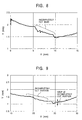
- the image output from the image reconfiguring circuit 180 is as shown in Fig. 7, and even though the contrast of the optical cutting image was extremely low at the cut portion, the fact that the cut was normal, and the manner in which the cut portion and uncut portion differ in curvature, could be observed. Also, the output image of the image reconfiguring circuit 180 while manufacturing a different electric resistance welded pipe 110 was as shown in Fig. 8, wherein it could be configured that the bead cutting was incomplete, due to some sort of cutting abnormality. A sample was collected of the bead cutting portion on the inner side of the pipe equivalent to Fig.
- Fig. 10 is a block diagram illustrating the configuration of the computation circuit group within the measurement head according to another embodiment of the present invention.
- the unshown bead trimmer 112 and measurement head 150 to be mounted thereupon are of the same configuration as those in the first embodiment, so description thereof will be omitted.
- first integration circuit 174 second computation circuit 176
- integration circuit 178 integration circuit 178
- image reconfiguring circuit 180 the same articles as those used in the above first embodiment may be employed here.
- Reference numeral 184 in the present embodiment denotes a branch circuit and 186 denotes a second integration circuit.
- the branch circuit 184 is a circuit for judging which of the maximum luminance I0 on the optical cutting line calculated by the first computation circuit 174, and the fixed threshold value J2 set beforehand, is greater, and causing one or the other of the first integration circuit 178 and the second integration circuit 186 to operate. This can be configured with a commercially-available comparator circuit.
- the threshold J1 of the integration circuit 178 in the above-described first embodiment is replaced with the predetermined fixed threshold value J2.
- the same image reconfiguring circuit 180 as that with the above-described first embodiment may be used, with the branch circuit 184 selecting either the first integration circuit 178 or the second integration circuit 184 as the input thereof.
- the image output from the image reconfiguring circuit 180 is as shown in Fig. 12, and the bead cutting shape could be measured suitably without effects of halation or noise.
- Fig. 15 illustrates around a bead trimmer 212 on the inner face of the electric resistance welded pipe 210, with reference numeral 214 denoting a cutting tool, 216 denoting a supporting arm, 250 denoting a measurement head of a bead cutting shape measurement device according to the present invention, 270 denoting a control device, 290 denoting a display device, and 292 denoting a recording device.
- the measurement head 250 is placed downstream in the pipe transportation direction of the cutting tool 214, preferably at a position 500 to 2000 mm therefrom, preferably has a mechanism for protecting the measurement equipment from radiant heat and welding sparks from the welding seam, and scattering of solution water, and preferably has a gas purging mechanism handling both cleansing and cooling, in order to prevent overheating of the optical system and soiling thereof by water, oil, fumes, and so forth.
- control device 270, display device 290, and recording device 292 are preferably positioned at a working position away form the manufacturing line, for example, near an operating board not shown in the drawings to be operated by an operator, and connected to the measurement head 250 by a cable 260 through a supporting arm 216 or the like, with a shielded configuration to prevent intrusion of electric noise along the way.
- the measurement method and device for the electric resistance welded pipe bead cutting shape according to the present invention may be equally applied to the outer face or the inner face of the pipe.
- reference numeral 220 denotes a slit light source
- 230 denotes a camera
- 232 denotes a lens
- 224 denotes light source power source
- 225 denotes camera power source
- 272 denotes an image data conversion circuit.
- the light source power source 224, camera power source 225, image data conversion circuit 272, and the later-described computation circuit group are preferably stored in one case as a control device 270.
- the computation circuit group is a thinning processing circuit 275 and an image synthesizing circuit 281.
- the slit light source 220 is within the measurement head 250 and irradiates a slit light 221 which has an angle ⁇ as to the cross-section of the electric resistance welded pipe 210, has a predetermined irradiation width in the pipe circumferential direction (width direction), and forms the irradiation width of a rectangular irradiated image as narrow as possible in the pipe axial direction, preferably 0.05 mm or less, and in this aspect, the present embodiment has the same arrangement as with conventional art.
- the camera 230 observes the irradiation image of the slit light irradiated onto the bead cutting portion from an angle ⁇ as to the cross-section of the electric resistance welded pipe 210, and ITVs or cameras using semiconductor devices such as CCD or CMOS which are widely used in industrial fields can be used.
- a commercially-available camera lens may be used for the lens 232 for image formation by the camera, but a bandpass filter having a passage wavelength band matching the wavelength of the light source in order to eliminate unnecessary light such as background light or the like from the optical cutting image, and a heat-ray cut filter or the like for preventing damage to the image-taking surface of the camera and the lens from radiant heat, should be provided as necessary.
- the measurement head 250 is preferably a sealed structure for protecting the optical equipment such as the camera 230, light source 220, lens 232, etc., within from heat and water and the like, and in this case, a preferably configuration has windows 252 and 254 for only the slit light and camera field of view portions, respectively.
- the position angle of the camera 230 is preferably such that ( ⁇ + ⁇ ) is generally 90°, with the number of pixels of the camera and the field of view being determined based on the width of the bead portion and the necessary resolution.
- the range of the field of view is 25 mm wide and 20 mm high
- the number of pixels is 1300 horizontally by 1000 vertically, as a suitable value.
- the light source 220 and camera 230 should be positioned such that the optical axes thereof intersect precisely over the bead cutting portion, and further, the plane formed by the axial axes of the light source 220 and camera 230 even more preferably contains the direction of progression of the electric resistance welded pipe 210, i.e., the center axis of the pipe.
- this arrangement of the light source and the camera allows the optical cutting image on the inner face of the pipe to be horizontally symmetrically taken with regard to a virtual center line extending in the Y-axial direction on the optical cutting image.
- the light source 220 and the camera 230 may be fixed to the measurement head 250 in an inclined state as shown in Fig. 16, or may be disposed so that their optical axes are both parallel to the central axis within the electric resistance welded pipe to reduce the size of the device, with the angle of the optical axis being changed by the reflection mirror 236.
- the image data conversion circuit 272 converts each pixel of image signals output form the camera 230 into luminance data and outputs, and an image board (frame-grabber) widely commercially available in recent years, which is compatible with the camera 230, can be used.
- the thinning processing circuit 275 is for performing thinning processing of the slit light image within the acquired picture. Either conventionally known thinning processing means, or the thinning processing method proposed here by the Inventors, may be used.
- the image synthesizing circuit 281 is for overlaying the slit light image picture subjected to thinning processing as described above, and the original optical cutting image (original image picture) output from the image data conversion circuit. Specifically, the image synthesizing circuit 281 performs computation such as addition of values of pixels on the same coordinates in the image, obtaining the logical OR, overwriting a thinning line alone on the original image picture, and so forth.
- Fig. 17 is an optical cutting image of a cut bead observed with the device according to the present embodiment at the time of manufacturing the electric resistance welded pipe 210
- Fig. 18 is the thinning processing results of the optical cutting image shown in Fig. 17.
- recessed notches occur in the thinning results as indicated by the arrows in Fig. 18, due to scattered light noise at the circled portions in Fig. 18.
- This can be told from the output of the present embodiment being as shown in Fig. 19.
- the original image picture and the thinning results can both be confirmed as shown in Fig. 19, so mistaking such notches due to scattered light noise for cutting steps can be avoided.
- Fig. 20 is a block diagram illustrating the configuration of the computation circuit group within the control device 270 according to another embodiment of the present invention.
- the unshown bead trimmer 212 and the measurement head 250 to be mounted thereupon are of the same configuration as those in the first embodiment, so description thereof will be omitted.
- the same image data conversion circuit 272 and thinning processing circuit 275 as the first embodiment may be used.
- the SN ratio detecting circuit 277 is for calculating the ratio between the luminance of the optical cutting line image and the luminance of a portion outside of the optical cutting line image, at the same X coordinate in the image at the time of performing thinning processing, for each X coordinate, and can be realized by combining a known maximum value searching circuit and dividing circuit.
- the thinning circuit 288 is for coloring each pixel on the thing line portion in the thinning image according to the SN ratio at each X coordinate, output by the SN ratio computation circuit, and may be colored with grayscale or an arbitrary color order.
- a preferred example of the present embodiment is arranged with colors corresponding to the SN ratio being assigned in 16 steps, as shown in Table 1. In Table 1, intermediate colors of commonly-known color names are frequently used, so the colors are also listed in the RGB luminance format, as well.
- Fig. 21 is an optical cutting image of a cut bead observed with the device according to the present embodiment while manufacturing the electric resistance welded pipe 210
- Fig. 22 and Fig. 23 are the results of thinning processing of the optical cutting image.
- the portions in Fig. 22 indicated by the arrows have marked protrusions in the thinning results, which are portions exhibiting abnormal values in the thinning processing due to the luminance of the slit light at this portion being very small, but these cannot be recognized with conventional lines alone being displayed.
- Fig. 23 is a thinning image output from the thinning circuit according to the present embodiment, which shows that the SN at the portions corresponding to the circled portions in Fig. 22 is at a minimal level (blue or blue-green) by the color of the thinning image. Accordingly, erroneously recognizing the cutting shape of this portion was prevented.
- Fig. 24 is a block diagram illustrating the configuration of the computation circuit group within the control device 270 of yet another embodiment according to the present invention.
- the unshown bead trimmer 212 and the measurement head 250 to be mounted thereupon are of the same configuration as those in the first embodiment, so description thereof will be omitted.
- the same image data conversion circuit 272 and thinning processing circuit 275 as the first embodiment may be used, and the same SN ratio detecting circuit 277 and thinning circuit 288 as the second embodiment may be used.
- Fig. 25 is an optical cutting image of a cut bead observed with the device according to the present embodiment while manufacturing the electric resistance welded pipe 210
- Fig. 26 is the results of thinning processing of the optical cutting image shown in the optical cutting image in Fig. 25.
- the portion in Fig. 26 indicated by the arrow has irregularities in the thinning results, which is a portion exhibiting abnormal values in the thinning processing due to the luminance of the slit light at this portion being very small, besides effects of scattering noise, but these cannot be recognized with conventional lines alone being displayed.
- Fig. 27 is a thinning image output from the thinning circuit according to the present embodiment, which shows that the SN at the portion corresponding to the circled portion in Fig. 26 is at a minimal level (blue or blue-green) by the color of the thinning image, and that has departed from the original optical cutting line image. Accordingly, mistaking this portion for a cutting step was prevented.
- all or part of the thinning circuit 275, the SN ration detection circuit 277, and the remaining image processing computation group, within the control device 270 may be realized by software, programs in ROM, etc., within a digital computer.
- Fig. 31 is a schematic diagram illustrating an example of an equipment configuration of a bead detecting device for a electric resistance welded pipe according to the present invention.
- reference numeral 320 denotes the electric resistance welded pipe, 301 denoting light projecting means, 302 denoting image-taking means, 303 denoting profile calculating device, 304 denoting a profile data processing device, and 305 denoting a display device.
- Fig. 32 is a configuration diagram illustrating the internal configuration of the profile data processing device 304.
- reference numeral 310 denotes a temporary apex calculating circuit
- 311 denotes a first regression computation circuit
- 312 denotes an intersecting point calculating circuit
- 313 denotes a first range calculating circuit
- 314 denotes a second regression computation circuit
- 315 denotes a deviation calculating circuit
- 316 denotes a second range calculating circuit.
- a slit light source wherein light emitted from a light emitting device such as a laser or lamp is converged at a line with a cylindrical lens or the like, or a scanning point light source wherein a light which converges at a point on an irradiation position is scanned in the width direction using a mirror or the like, may be used, but a small-size slit light source wherein a light emitting diode(LED) and a lens system are integrated is preferably used, the width of the short side of the slit is preferably sufficiently smaller than the height of the welding bead, preferably 50 ⁇ m or smaller.
- the shape of the portion to be measured is calculated as a single line by the later-described optical cross-sectional image processing, so this is not indispensable but should be as small as practicable.
- ITV cameras or a PSD Position Sensitive Device, an optical position detecting device
- a CCD camera taking the ease of data conversion to the following image processing device, a CCD camera is suitably used.
- common arrangements may be selected and used for the lens mechanism for forming an image from irradiated light, the aperture diaphragm for adjusting the amount of light received to an appropriate range, the shutter mechanism, and so forth.
- the incident angle ⁇ of the light projecting means 301 serving as the light source, and the mounting angle of the image-taking means 302, i.e., the image-taking angle ⁇ , is preferably such that ( ⁇ + ⁇ ) is generally 90°, with the number of pixels and the field of view of the camera, i.e., the image-taking means 302 being determined based on the width of the bead portion and the necessary resolution.
- the range of the field of view is 25 mm wide and 20 mm high
- the number of pixels is 640 horizontally by 480 vertically.
- the profile calculating means 303 is for converting a slit light image projected on the pipe surface as shown in Fig. 33 into one line with appropriate image processing means, and further calculating a true profile in the wall thickness cross-sectional direction of the pipe, i.e., profile data of the electric resistance welded pipe, based on the slit light image, i.e., a pseudo-cross-sectional profile, from the placement of the light source and the image-taking means, i.e., from geometric calculations of the incident angle ⁇ and the image-taking angle ⁇ .
- a true profile in the wall thickness cross-sectional direction of the pipe i.e., profile data of the electric resistance welded pipe
- a true profile in the wall thickness cross-sectional direction of the pipe i.e., profile data of the electric resistance welded pipe
- a true profile in the wall thickness cross-sectional direction of the pipe i.e., profile data of the electric resistance welded pipe
- the profile data processing device 304 With the direction crossing the bead portion (width direction) as the X axis in a pseudo-cross-sectional profile obtained by irradiation of slit light as described above, or a profile of the electric resistance welded pipe, following thinning processing in either case, the profile can be represented as a data group of heights corresponding to X coordinates.
- the temporary apex calculating circuit 310 calculates the apex position Xc0 of the welding bead, so a configuration for calculating the weighted mean (position of the first order moment) of the profile data, for example, is sufficient.
- this can be performed by stringing pixels exhibiting the maximum luminance with regard to a given width-direction (X-axial direction) coordinate, in the width direction (X-axial direction), and obtaining the X coordinate exhibiting the maximum value on the vertical axis from these.
- the first regression computation circuit 311 is for regression of the profile data such as shown in Fig. 34 with a quadratic function, so a configuration for executing known regression computation, preferably least-square computation, is sufficient.
- a first approximation curve wherein the first regression computation circuit 311 has approximated the profile data with a quadratic function is shown in Fig. 35.
- Fig. 34 uses relative values for the height of the bead shown on the vertical axis. This means values wherein the geometric part are omitted, with regard to the fact that the above-described geometric calculation part may be omitted without any particular problem for the bead shape detection which is an object of the present invention since the profile data of the electric resistance welded pipe is simple, as described earlier. This understanding holds in the following description.
- the intersecting point calculating circuit 312 selects, of the points where the profile data and the first approximation curve intersect, the two closest points on the left side and right side of the apex Xc0, as X1 and Xr, respectively, as shown in Fig. 35.
- the first range calculating circuit 313 calculates the range of the coordinates used for the following base pipe regression, based on the X1 and Xr calculated by the intersecting point calculating circuit 312, and the apex Xc0. For example, a suitable example is to calculate R: x ⁇ X1', x > Xr' based on the 3 : 2 externally dividing point of the apex and intersecting points.
- X1' (3X1 - Xc0)/2
- Xr' (3Xr - Xc0)/2
- This external dividing ratio should be decided as appropriate, taking into consideration the smoothness of the slope of an average bead, based on experience, for example.
- the second regression computation circuit 314 performs least-square polynomial regression computation in the range R for x that has been calculated as described above, as with the first regression computation circuit, is sufficient.
- the polynomial used for calculations at the second regression computation circuit 314 is a polynomial of an even degree quadratic or higher, and preferably is a quartic or higher polynomial. This yields the second approximation curve. This second approximation curve is extrapolated into the region X1' ⁇ x ⁇ Xr' outside of the range R for the above-described x, as well.
- the deviation calculating circuit 315 is for calculating the deviation between the second approximation curve output by the second regression computation circuit and the profile data of the electric resistance welded pipe, over the entirety of X coordinates where profile data of the electric resistance welded pipe exists ("entirety" meaning within the image field of view as an optical cutting image), and can be configured of a polynomial computation circuit and a subtraction circuit.
- the second range calculating circuit 316 then calculates the range where the output of the deviation calculating circuit 315 exceeds the predetermined threshold value and outputs the portion of this range containing the apex Xc0 as a temporary existence range for the bead, and can be configured of a threshold circuit and a comparator circuit.
- the optical cutting image obtained by the light projecting means 301 irradiating slit light onto the surface of the pipe and taking an image thereof with the image-taking device 302 is as shown in Fig. 33, and the profile data of the electric resistance welded pipe including the bead portion calculated by the profile calculating means 303 from this optical cutting image that has been subjected to thinning processing is as shown in Fig. 34.
- the temporary apex calculating circuit 310 calculates the apex by a technique such as maximum value computation, weighted mean (center of gravity computation), etc., with regard to this profile data.
- the Xc0 marked in Fig. 34 is the apex position of the bead thus calculated.
- the first regression computation circuit 311 performs least-square regression computation by the quadratic expression of the entire profile, consequently outputting a quadratic function as shown in Fig. 35.
- the X1, Xr, X1', and Xr' marked in Fig. 35 in the same way are positions of X coordinates calculated by the intersecting point calculating circuit 312 and range calculating circuit 313, as described above.
- the second regression computation circuit 314 calculates the second approximation curve for the profile data regarding the range of the X coordinates set by the range calculating circuit 313.
- the quartic degree was selected as a suitable example for regression.
- the second approximation curve obtained as a result is as shown in Fig. 36 by the heavy line.
- the deviation calculating circuit 315 calculates the deviation e(x) between the heavy line in Fig. 36 and the profile data of the electric resistance welded pipe, and the results thereof are obtained as shown in Fig. 37.
- the second range calculating circuit 316 searches for ranges wherein this deviation e(x) exceeds a threshold value set beforehand, and of these, calculates a range of X coordinates including the apex coordinates Xc0.
- a threshold value of 0.05 was used as a suitable example in the present embodiment. The results thereof indicate the range marked by the arrows in Fig. 37.
- the internal configuration circuits of the profile calculating device 303 and profile data processing device 304 may be realized by software or programs in ROM, within a digital computer.
- the object of application of the present invention is not restricted to steel pipe, and may be other metal pipes, such as copper, aluminum, and so forth.
- Fig. 40 is a schematic diagram illustrating a configuration example of a electric resistance welded pipe bead shape detecting device according to the present invention.
- reference numeral 420 denotes the electric resistance welded pipe, with 401 denoting light projecting means, 402 denoting image-taking means, 403 denoting bead shape calculating means, 404 denoting a data processing device, and 405 denoting a display device.
- a slit light source wherein light emitted from a light emitting device such as a laser or lamp is converged on a plane with a cylindrical lens or the like, or a scanning point light source wherein a light which converges at a point on an irradiation position is scanned in the width direction using a mirror or the like, may be used, but a small-size slit light source wherein a semiconductor device (LED) and a lens system are integrated is preferably used, the width of the short side of the slit is preferably sufficiently smaller than the height of the welding bead, preferably 50 ⁇ m or smaller.
- the shape of the portion to be measured is calculated as a single line by the later-described optical image processing, so this is not indispensable.
- ITV cameras or a PSD Position Sensitive Device, an optical position detecting device
- a CCD camera taking the ease of data conversion to the following image processing device, a CCD camera is suitably used.
- common arrangements may be selected and used for the lens mechanism for forming an image from irradiated light, the aperture diaphragm for adjusting the amount of light received to an appropriate range, the shutter mechanism, and so forth.
- the incident angle ⁇ of the light projecting means 401, and the mounting angle ⁇ of the image-taking means 402, is preferably such that ( ⁇ + ⁇ ) is generally 90°, with the number of pixels and the field of view of the camera, being determined based on the width of the bead portion and the necessary resolution.
- the range of the field of view is 25 mm wide and 20 mm high
- the number of pixels is 640 horizontally by 480 vertically.
- the bead shape calculating means 403 are for taking the slit light image as one line with suitable image processing means, and calculating a bead shape (profile) by geometric calculations determined by the positioning of the light projecting means 401 and the image-taking means 402.
- a profile refers to the outline shape on the inner face or output face of the electric resistance welded pipe, and the shape data of the pipe surface including the bead portion is from a section thereof.
- thinning processing may be used for the image processing means here, but the thinning processing means proposed by the Inventors here is preferably used.
- the internal configuration of the data processing device 404 is shown in Fig. 41, comprising a apex position setting circuit 410, a bead range setting circuit 411, a bead shape approximation circuit 412, a base pipe shape approximation circuit 413, a bead range re-setting circuit 414, and a features calculating circuit 415.
- the following is a description of the components of the data processing device 404.
- the apex position setting circuit 410 sets the apex position of the bead from shape data of the pipe surface including the bead portion calculated as described above.
- An arrangement may be made wherein an operator judges and manually inputs the apex position of the bead from the shape data of the pipe surface containing the bead portion, but a more preferable arrangement is to obtain a position indicating the maximum height value in the shape data of the pipe surface containing the bead portion. Further, this can by calculated with addition processing by weighted mean computation or the like.
- the bead range setting circuit 411 sets a bead range from shape data of the pipe surface including the bead portion, calculated as described above.
- An arrangement may be made wherein an operator judges the bead range from the shape data of the pipe surface containing the bead portion and manually inputs the boundaries at the left and right edges of the bead portion, and sets the region equivalent to the portion between left and right boundaries as the bead range, or an arrangement wherein the slope position is detected based on difference in adjacent shape data, such as disclosed in Patent Document 3, but a more preferable arrangement is to divide a preset bead width into two halves centered on the bead apex position output from the apex position setting circuit 410, or to set following the method disclosed in the electric resistance welded pipe bead shape detecting method which the Inventors propose here.
- the bead shape approximation circuit 412 divides the bead range which is set as described above into the left side of the apex x 1 ⁇ x ⁇ x c and the right side of the apex x c ⁇ x ⁇ x r , approximates the shape of the bead portion in each range with a predetermined function, and determines the function with regard to the shape of the left and right portions of the bead portion.
- a preferred method thereof will be described in the section on the operations of the present embodiment, later.
- the base pipe shape approximation circuit 413 is for approximating the shape data of the bead range thus set with pipe surface shape data, wherein the shape data of the bead range is removed from the shape data of the pipe surface including the bead portion, and a function of a predetermined form such as a power function or the like, and specific parameters such as the coefficients of the functions are calculated.
- a preferred method thereof will be described in the section on the operations of the present embodiment, later.
- the bead range re-setting circuit 414 is for re-recognizing the positions where the values of the approximation functions of the thus-determined left and right bead shape and the approximation function of the base pipe shape intersect as the boundary positions between the bead portion and the base pipe position, and can be configured from a function value computation circuit and a comparator.
- the features calculating circuit 415 is for calculating the bead width, height, left and right slope angles, and unevenness between the boundary between the left and right bead portions and the base pipe portion, based on the thus-calculated bead range, apex position, approximation functions for the left and right bead shapes, approximation function for the base pipe shape, and shape data of the pipe surface including the bead portion.
- the display device 405 displays the features of the bead shape detected by the features calculating circuit 415. While each of the values may be periodically updated and displayed as numbers or bar charts, a preferable arrangement is to display the shape data of the pipe surface including the bead portion and the features of each as a time chart.
- an arrangement may be made wherein the output for the features calculating circuit 415 is output to an unshown recorder or business computer or the like by an unshown communication port or external output circuit, at appropriate time intervals, so as to accumulate data.
- Fig. 42 is an optical cutting image of the slit light source 401 serving as the light projecting means covering the range of the pipe surface including the bead portion, taken with the image-taking means 402, and the results of subjecting this to thinning processing with the bead shape calculating means 403 and converting into coordinates on the display device 405 is the shape data of the pipe surface including the bead portion such as shown in Fig. 43.
- the arrows marked in Fig. 43 indicate the bead range calculated by the apex position setting circuit 410 and the bead range setting circuit 411, and the x coordinate at the apex position.
- i L and i R are shape data addresses for the left edge and right edge of the bead range.
- the i c used below is an address for a shape data row equivalent to the x c obtained as described above.
- E L the least value of E L is to be solved regarding the five parameters of a L1 , b L1 , a L2 , b L2 , and x p1 , in order to calculate f L (x), which can be calculated by dividing into the following steps.
- the base pipe shape approximation circuit 413 calculates the approximation function f p (x) with regard to the range excluding the bead portion. Though a circle or ellipse may be used for this approximation function f p (x), a power function, and an even degree polynomial, quadratic or higher, is preferably used as the approximation curve.
- Fig. 45 is a chart illustrating the relation between the degree of a polynomial and the RMS (root-mean-square) of approximation error, in a case of regression of the upper half curve of a circle with quadratic, quartic, sextic, and octic polynomials, indicating that a polynomial of an even degree quadratic or higher, and preferably a quartic or higher polynomial, can perform regression of the shape of the ellipse with sufficient precision. Accordingly, with the present embodiment, approximation is performed with a quartic function.
- the bead range re-setting circuit 414 calculates the intersecting points of the left and right bead shape approximation functions f L (x) and f R (x) calculated as described above with the base pipe shape approximation function f p (x), and outputs the region corresponding to between the calculated left and right intersecting points as a new bead range (x L ', x R ').
- the dashed line plotted in Fig. 46 is the shape data of the pipe surface including the bead portion, the same as that shown in Fig. 43.
- the features calculating circuit 415 calculates the bead height H, width W, slope angles ⁇ L and ⁇ R of the left and right bead portions, and the unevenness ⁇ between the left and right bead portion boundaries, from the thus-calculated bead range, apex position, approximation functions for the left and right bead shapes, approximation function for the base pipe, and the shape data of the pipe surface including the bead portion.
- the present embodiment performs calculations following the following definitions.
Landscapes
- Engineering & Computer Science (AREA)
- Mechanical Engineering (AREA)
- Physics & Mathematics (AREA)
- General Physics & Mathematics (AREA)
- Length Measuring Devices By Optical Means (AREA)
Applications Claiming Priority (9)
| Application Number | Priority Date | Filing Date | Title |
|---|---|---|---|
| JP2002128497A JP3823871B2 (ja) | 2002-04-30 | 2002-04-30 | 電縫溶接管のビード切削形状の計測方法および装置 |
| JP2002128497 | 2002-04-30 | ||
| JP2002251269 | 2002-08-29 | ||
| JP2002251269A JP2004093195A (ja) | 2002-08-29 | 2002-08-29 | 電縫溶接管の溶接ビード切削形状計測方法および計測装置 |
| JP2002277802A JP3858792B2 (ja) | 2002-09-24 | 2002-09-24 | 電縫溶接管のビード形状検出方法および検出装置 |
| JP2002277802 | 2002-09-24 | ||
| JP2002348649 | 2002-11-29 | ||
| JP2002348649A JP4374845B2 (ja) | 2002-11-29 | 2002-11-29 | 電縫溶接管のビード形状検出方法および装置 |
| PCT/JP2003/005168 WO2003093761A1 (fr) | 2002-04-30 | 2003-04-23 | Procede et instrument de mesure de la forme de coupe du manchon de verre d'un tube electrique soude |
Publications (3)
| Publication Number | Publication Date |
|---|---|
| EP1500904A1 true EP1500904A1 (fr) | 2005-01-26 |
| EP1500904A4 EP1500904A4 (fr) | 2008-08-27 |
| EP1500904B1 EP1500904B1 (fr) | 2010-09-29 |
Family
ID=29407968
Family Applications (1)
| Application Number | Title | Priority Date | Filing Date |
|---|---|---|---|
| EP03719173A Expired - Fee Related EP1500904B1 (fr) | 2002-04-30 | 2003-04-23 | Procede et dispositif de mesure de la forme de la coupe d'un tube soude electriquement |
Country Status (7)
| Country | Link |
|---|---|
| US (3) | US7236255B2 (fr) |
| EP (1) | EP1500904B1 (fr) |
| KR (1) | KR100685206B1 (fr) |
| DE (1) | DE60334373D1 (fr) |
| MY (1) | MY137246A (fr) |
| TW (1) | TW587153B (fr) |
| WO (1) | WO2003093761A1 (fr) |
Cited By (3)
| Publication number | Priority date | Publication date | Assignee | Title |
|---|---|---|---|---|
| DE102010013472B4 (de) * | 2010-03-30 | 2012-12-13 | Ernst Blissenbach Gmbh | Nahtüberwachungs-Vorrichtung |
| RU2606901C2 (ru) * | 2012-08-10 | 2017-01-10 | Смс Груп Гмбх | Способ и устройство для оптического измерения внутренних размеров трубы |
| CN112489010A (zh) * | 2020-11-27 | 2021-03-12 | 桂林电子科技大学 | 一种焊缝快速识别方法、装置及存储介质 |
Families Citing this family (42)
| Publication number | Priority date | Publication date | Assignee | Title |
|---|---|---|---|---|
| US6440425B1 (en) | 1995-05-01 | 2002-08-27 | Aventis Pasteur Limited | High molecular weight major outer membrane protein of moraxella |
| JP4544240B2 (ja) * | 2005-11-21 | 2010-09-15 | Jfeスチール株式会社 | 管体の超音波探傷装置および超音波探傷方法 |
| KR100797239B1 (ko) * | 2005-12-23 | 2008-01-23 | 주식회사 포스코 | 강판의 용접부 온라인 검출장치 및 방법 |
| US8118733B2 (en) * | 2006-12-22 | 2012-02-21 | Ge Inspection Technologies, Lp | Heat protection systems and methods for remote viewing devices |
| JP4861854B2 (ja) * | 2007-02-15 | 2012-01-25 | 株式会社バンダイナムコゲームス | 指示位置演算システム、指示体及びゲームシステム |
| DE102007011394A1 (de) * | 2007-03-07 | 2008-09-11 | Fachhochschule Kiel | Verfahren zur Messung der Fließgeschwindigkeit eines Mediums unter Anlegen eines Magnetfelds an das durchsetzte Meßvolumen |
| BRPI0818126A2 (pt) * | 2007-11-02 | 2020-10-06 | Nippon Steel Corporation | sistema e método para monitoramento de estado de soldagem |
| CN102066040B (zh) * | 2008-06-23 | 2015-08-12 | 杰富意钢铁株式会社 | 激光焊接钢管的制造方法 |
| US8657605B2 (en) * | 2009-07-10 | 2014-02-25 | Lincoln Global, Inc. | Virtual testing and inspection of a virtual weldment |
| US8917320B2 (en) | 2009-03-04 | 2014-12-23 | VISIONx INC. | Digital optical comparator |
| JP5178624B2 (ja) * | 2009-05-11 | 2013-04-10 | 株式会社日立製作所 | 解析モデル生成装置 |
| US8004695B1 (en) * | 2010-08-16 | 2011-08-23 | Paccar Inc. | Measurement of film thickness in motor exhaust systems |
| JP5672480B2 (ja) * | 2010-08-30 | 2015-02-18 | スズキ株式会社 | ビードの終端部の形状を判定する装置及びその方法 |
| DE102011109717B3 (de) * | 2011-08-06 | 2012-10-11 | Ndt Systems & Services Gmbh & Co. Kg | Verfahren und Sensorträger zur Aufdachungsmessung von Rohrleitungen mittels Ultraschallprüfung |
| JP5494597B2 (ja) * | 2011-09-16 | 2014-05-14 | 株式会社安川電機 | ロボットシステム |
| US9764415B2 (en) * | 2013-03-15 | 2017-09-19 | The United States Of America As Represented By The Administrator Of Nasa | Height control and deposition measurement for the electron beam free form fabrication (EBF3) process |
| US9267784B2 (en) | 2013-07-15 | 2016-02-23 | Faro Technologies, Inc. | Laser line probe having improved high dynamic range |
| FR3011935B1 (fr) * | 2013-10-11 | 2017-06-23 | Luceo | Procede et dispositif pour inspecter les soudures d'emballages |
| US9658061B2 (en) | 2013-12-31 | 2017-05-23 | Faro Technologies, Inc. | Line scanner that uses a color image sensor to improve dynamic range |
| US9531967B2 (en) | 2013-12-31 | 2016-12-27 | Faro Technologies, Inc. | Dynamic range of a line scanner having a photosensitive array that provides variable exposure |
| KR101599154B1 (ko) * | 2014-11-07 | 2016-03-02 | 두산중공업 주식회사 | 용접량 측정 장치 및 방법 |
| US10019666B2 (en) * | 2015-03-10 | 2018-07-10 | Primetals Technologies Germany Gmbh | Counting bar-shaped products based upon acquired images |
| WO2017119118A1 (fr) * | 2016-01-08 | 2017-07-13 | オリンパス株式会社 | Procédé et appareil de mesure de forme d'échantillon |
| JP6159005B1 (ja) * | 2016-11-21 | 2017-07-05 | 株式会社中田製作所 | 溶接管製造装置および溶接管製造方法 |
| DE102017102762B4 (de) * | 2017-02-13 | 2023-06-15 | Precitec Gmbh & Co. Kg | Verfahren zum Erkennen von Fügepositionen von Werkstücken und Laserbearbeitungskopf mit einer Vorrichtung zur Durchführung dieses Verfahrens |
| US11440125B2 (en) * | 2018-03-29 | 2022-09-13 | Jfe Steel Corporation | Electric resistance welded steel pipe for producing hollow stabilizer, hollow stabilizer, and production methods for same |
| CN108876771B (zh) * | 2018-06-04 | 2022-05-20 | 广东工业大学 | 一种咬边焊接缺陷的检测方法 |
| TWI673620B (zh) * | 2018-11-28 | 2019-10-01 | 財團法人工業技術研究院 | 利用動態位置誤差模擬切削方法 |
| CN111612730B (zh) * | 2019-02-23 | 2022-04-22 | 妙微(杭州)科技有限公司 | 一种焊缝检测定位方法 |
| JP7247876B2 (ja) * | 2019-12-10 | 2023-03-29 | トヨタ自動車株式会社 | 溶着ビード切削装置および溶着ビード切削方法 |
| CN112132807B (zh) * | 2020-09-23 | 2024-02-23 | 泉州装备制造研究所 | 一种基于颜色相似度分割的焊缝区域提取方法和装置 |
| CN113592798B (zh) * | 2021-07-21 | 2023-08-15 | 山东理工大学 | 一种道路病害智能辨识方法、系统、终端及介质 |
| US11828190B2 (en) | 2021-11-18 | 2023-11-28 | General Electric Company | Airfoil joining apparatus and methods |
| KR102562216B1 (ko) * | 2021-11-29 | 2023-08-01 | 한국광기술원 | 용접 비드의 3차원 형상 검사 시스템 및 그 방법 |
| CN114577122B (zh) * | 2022-02-28 | 2023-08-18 | 长三角先进材料研究院 | 一种基于图像处理的自冲铆接剖面几何参数自动测量方法 |
| CN114769715B (zh) * | 2022-04-25 | 2023-07-07 | 湖南机电职业技术学院 | 轨道式大直径管道切割装置 |
| CN114782526B (zh) * | 2022-06-22 | 2022-09-02 | 季华实验室 | H型钢的焊缝轨迹计算方法、装置、电子设备及存储介质 |
| CN115319323B (zh) * | 2022-07-27 | 2024-03-29 | 熵智科技(深圳)有限公司 | 管板焊焊接方法、系统、焊接机器人及存储介质 |
| TWI822209B (zh) * | 2022-07-28 | 2023-11-11 | 行政院原子能委員會核能研究所 | 銲接品質檢測裝置 |
| CN115338556A (zh) * | 2022-08-03 | 2022-11-15 | 湖南科技大学 | 用于厚壁焊接工件的焊缝质量检测方法及计算机设备 |
| CN116030098B (zh) * | 2023-03-27 | 2023-06-13 | 齐鲁工业大学(山东省科学院) | 一种基于方向特征驱动的焊缝目标跟踪方法及系统 |
| CN117557553B (zh) * | 2023-12-28 | 2024-05-24 | 中核武汉核电运行技术股份有限公司 | 一种核电站管道焊缝检测方法及装置 |
Citations (6)
| Publication number | Priority date | Publication date | Assignee | Title |
|---|---|---|---|---|
| JPH03289505A (ja) * | 1990-04-06 | 1991-12-19 | Nippondenso Co Ltd | 3次元形状測定装置 |
| EP0532257A2 (fr) * | 1991-09-11 | 1993-03-17 | Toyota Jidosha Kabushiki Kaisha | Appareil pour déterminer la qualité de cordon de soudure |
| JPH06241740A (ja) * | 1993-02-17 | 1994-09-02 | Nippon Steel Corp | 電縫管溶接ビード切削不良・欠陥検出方法 |
| JPH0740049A (ja) * | 1993-07-29 | 1995-02-10 | Nippon Steel Corp | Uo鋼管の溶接部検出方法及び装置 |
| JPH11230721A (ja) * | 1998-02-13 | 1999-08-27 | Fuji Xerox Co Ltd | 3次元形状計測装置および画像読取装置 |
| JPH11271029A (ja) * | 1998-03-23 | 1999-10-05 | Suzuki Motor Corp | 三次元形状の計測装置 |
Family Cites Families (23)
| Publication number | Priority date | Publication date | Assignee | Title |
|---|---|---|---|---|
| US4142713A (en) * | 1974-11-26 | 1979-03-06 | Nippon Steel Corporation | Method of heat-treatment of welded pipe and apparatus therefor |
| JPS606755B2 (ja) * | 1981-02-20 | 1985-02-20 | 日本鋼管株式会社 | 溶接管の外面溶接部断面形状検出装置 |
| JPS6025234B2 (ja) * | 1981-06-11 | 1985-06-17 | 日本鋼管株式会社 | 電縫溶接管の溶接部メタルフロ−角度測定方法 |
| JPS57208404A (en) | 1981-06-19 | 1982-12-21 | Hitachi Ltd | Configuration detecting method |
| US4645893A (en) * | 1983-06-23 | 1987-02-24 | Nippon Steel Corporation | Method for manufacturing spiral-welded steel pipe |
| JPS60128304A (ja) * | 1983-12-15 | 1985-07-09 | Nippon Tsushin Gijutsu Kk | 溶接機計測ヘツド |
| JPS61111461A (ja) * | 1984-11-06 | 1986-05-29 | Nippon Steel Corp | 電縫管溶接部の超音波探傷方法 |
| US4734766A (en) * | 1985-08-19 | 1988-03-29 | Kawasaki Steel Corporation | Method and system for locating and inspecting seam weld in metal seam-welded pipe |
| DE3632952A1 (de) * | 1986-09-27 | 1988-04-07 | Hoesch Ag | Verfahren und vorrichtung zur kontinuierlichen herstellung rohrfoermiger koerper mittels laser-laengsnahtschweissung |
| JPH0235306A (ja) | 1988-07-26 | 1990-02-05 | Mitsubishi Electric Corp | 形状検出方法 |
| JPH03234444A (ja) * | 1990-02-09 | 1991-10-18 | Nkk Corp | 電縫管内面ビード切削状況監視装置 |
| JPH04122811A (ja) * | 1990-09-14 | 1992-04-23 | Sumitomo Metal Ind Ltd | 管内面ビード切削異常監視装置 |
| JPH04240508A (ja) | 1991-01-23 | 1992-08-27 | Mitsubishi Heavy Ind Ltd | 三次元形状認識装置 |
| US5331770A (en) * | 1991-07-26 | 1994-07-26 | Hitachi, Ltd. | Method for scraping off excessive portion of workpiece |
| JP2618303B2 (ja) | 1991-09-26 | 1997-06-11 | 新日本製鐵株式会社 | 電縫管溶接ビード切削形状計測方法 |
| JPH08292017A (ja) | 1995-04-25 | 1996-11-05 | Tokai Rika Co Ltd | 断面形状選別装置 |
| US5681490A (en) * | 1995-09-18 | 1997-10-28 | Chang; Dale U. | Laser weld quality monitoring system |
| JP3151790B2 (ja) | 1995-09-27 | 2001-04-03 | 川崎製鉄株式会社 | 溶接開先・ビードの中心位置検出方法及び装置 |
| WO1998034195A1 (fr) * | 1997-01-30 | 1998-08-06 | Yissum Research Development Company Of The Hebrew University Of Jerusalem | Mosaique panoramique generalisee |
| JPH11194103A (ja) * | 1998-01-06 | 1999-07-21 | Hitachi Eng & Service Co Ltd | 電縫管内の異物検出方法、異物表示装置ならびに電縫管 |
| JPH11281343A (ja) * | 1998-03-30 | 1999-10-15 | Nippon Steel Corp | パイプ用外周長計測装置 |
| JP3678056B2 (ja) * | 1999-06-01 | 2005-08-03 | 日産自動車株式会社 | 溶接品質判定方法及び装置 |
| JP2002236100A (ja) * | 2001-02-09 | 2002-08-23 | Hitachi Ltd | 非破壊検査方法およびその装置 |
-
2003
- 2003-04-17 MY MYPI20031453A patent/MY137246A/en unknown
- 2003-04-23 KR KR1020047016653A patent/KR100685206B1/ko active IP Right Grant
- 2003-04-23 DE DE60334373T patent/DE60334373D1/de not_active Expired - Lifetime
- 2003-04-23 EP EP03719173A patent/EP1500904B1/fr not_active Expired - Fee Related
- 2003-04-23 US US10/507,350 patent/US7236255B2/en not_active Expired - Lifetime
- 2003-04-23 WO PCT/JP2003/005168 patent/WO2003093761A1/fr active Application Filing
- 2003-04-25 TW TW092109761A patent/TW587153B/zh not_active IP Right Cessation
-
2007
- 2007-05-21 US US11/802,133 patent/US7471400B2/en not_active Expired - Fee Related
-
2008
- 2008-05-01 US US12/113,440 patent/US7619750B2/en not_active Expired - Fee Related
Patent Citations (6)
| Publication number | Priority date | Publication date | Assignee | Title |
|---|---|---|---|---|
| JPH03289505A (ja) * | 1990-04-06 | 1991-12-19 | Nippondenso Co Ltd | 3次元形状測定装置 |
| EP0532257A2 (fr) * | 1991-09-11 | 1993-03-17 | Toyota Jidosha Kabushiki Kaisha | Appareil pour déterminer la qualité de cordon de soudure |
| JPH06241740A (ja) * | 1993-02-17 | 1994-09-02 | Nippon Steel Corp | 電縫管溶接ビード切削不良・欠陥検出方法 |
| JPH0740049A (ja) * | 1993-07-29 | 1995-02-10 | Nippon Steel Corp | Uo鋼管の溶接部検出方法及び装置 |
| JPH11230721A (ja) * | 1998-02-13 | 1999-08-27 | Fuji Xerox Co Ltd | 3次元形状計測装置および画像読取装置 |
| JPH11271029A (ja) * | 1998-03-23 | 1999-10-05 | Suzuki Motor Corp | 三次元形状の計測装置 |
Non-Patent Citations (1)
| Title |
|---|
| See also references of WO03093761A1 * |
Cited By (3)
| Publication number | Priority date | Publication date | Assignee | Title |
|---|---|---|---|---|
| DE102010013472B4 (de) * | 2010-03-30 | 2012-12-13 | Ernst Blissenbach Gmbh | Nahtüberwachungs-Vorrichtung |
| RU2606901C2 (ru) * | 2012-08-10 | 2017-01-10 | Смс Груп Гмбх | Способ и устройство для оптического измерения внутренних размеров трубы |
| CN112489010A (zh) * | 2020-11-27 | 2021-03-12 | 桂林电子科技大学 | 一种焊缝快速识别方法、装置及存储介质 |
Also Published As
| Publication number | Publication date |
|---|---|
| TW587153B (en) | 2004-05-11 |
| EP1500904A4 (fr) | 2008-08-27 |
| WO2003093761A1 (fr) | 2003-11-13 |
| US7236255B2 (en) | 2007-06-26 |
| US7619750B2 (en) | 2009-11-17 |
| US20080218768A1 (en) | 2008-09-11 |
| TW200402524A (en) | 2004-02-16 |
| KR100685206B1 (ko) | 2007-02-22 |
| EP1500904B1 (fr) | 2010-09-29 |
| DE60334373D1 (de) | 2010-11-11 |
| US7471400B2 (en) | 2008-12-30 |
| US20050147289A1 (en) | 2005-07-07 |
| MY137246A (en) | 2009-01-30 |
| KR20040101519A (ko) | 2004-12-02 |
| US20080105731A1 (en) | 2008-05-08 |
Similar Documents
| Publication | Publication Date | Title |
|---|---|---|
| US7236255B2 (en) | Method and instrument for measuring bead cutting shape of electric welded tube | |
| JP4705479B2 (ja) | ビード形状検出方法及び装置 | |
| EP1524492B1 (fr) | Dispositif de mesure en trois dimensions | |
| JP2017053790A (ja) | 欠陥検出装置及び欠陥検出方法 | |
| US20100157043A1 (en) | System and method for inspecting the interior surface of a pipeline | |
| JP5288297B2 (ja) | ねじ付き管の端部形状測定方法 | |
| US9638606B2 (en) | Tire shape inspection method and tire shape inspection device | |
| JP4893788B2 (ja) | 熱交換器のチューブ抽出検査方法及び装置 | |
| JP4876599B2 (ja) | 突合せ溶接部の良否検出方法および装置 | |
| JP3858792B2 (ja) | 電縫溶接管のビード形状検出方法および検出装置 | |
| JP4762851B2 (ja) | 断面形状検出方法及び装置 | |
| JP3823871B2 (ja) | 電縫溶接管のビード切削形状の計測方法および装置 | |
| JP4374845B2 (ja) | 電縫溶接管のビード形状検出方法および装置 | |
| Li et al. | On-line visual measurement and inspection of weld bead using structured light | |
| JP2004093195A (ja) | 電縫溶接管の溶接ビード切削形状計測方法および計測装置 | |
| JP4793161B2 (ja) | 突合せ溶接部の良否検査方法および装置 | |
| JP3137254B2 (ja) | 自動溶接方法 | |
| JPH05240620A (ja) | 管の外径・肉厚測定装置 | |
| JP2865125B2 (ja) | 電縫管溶接部の検査方法及び電縫管溶接部の検査装置 | |
| JPH1133621A (ja) | 溶接温度測定方法及び装置並びに溶接管製造方法及び装置 | |
| TWI711801B (zh) | 帶狀產品孔洞位置的檢測方法 | |
| JP2618303B2 (ja) | 電縫管溶接ビード切削形状計測方法 | |
| JP6064754B2 (ja) | 電縫鋼管の外表面形状計測方法および外表面形状計測装置 | |
| JPH05240619A (ja) | 管の外径・肉厚測定装置 | |
| JPH0577062A (ja) | 熱間電縫管溶接部の監視方法とその装置 |
Legal Events
| Date | Code | Title | Description |
|---|---|---|---|
| PUAI | Public reference made under article 153(3) epc to a published international application that has entered the european phase |
Free format text: ORIGINAL CODE: 0009012 |
|
| 17P | Request for examination filed |
Effective date: 20040915 |
|
| AK | Designated contracting states |
Kind code of ref document: A1 Designated state(s): AT BE BG CH CY CZ DE DK EE ES FI FR GB GR HU IE IT LI LU MC NL PT RO SE SI SK TR |
|
| A4 | Supplementary search report drawn up and despatched |
Effective date: 20080725 |
|
| 17Q | First examination report despatched |
Effective date: 20080925 |
|
| GRAP | Despatch of communication of intention to grant a patent |
Free format text: ORIGINAL CODE: EPIDOSNIGR1 |
|
| RTI1 | Title (correction) |
Free format text: METHOD OF AND DEVICE FOR MEASURING BEAD CUTTING SHAPE OF ELECTRIC WELDED TUBE |
|
| GRAS | Grant fee paid |
Free format text: ORIGINAL CODE: EPIDOSNIGR3 |
|
| GRAA | (expected) grant |
Free format text: ORIGINAL CODE: 0009210 |
|
| AK | Designated contracting states |
Kind code of ref document: B1 Designated state(s): DE FR |
|
| REF | Corresponds to: |
Ref document number: 60334373 Country of ref document: DE Date of ref document: 20101111 Kind code of ref document: P |
|
| PLBE | No opposition filed within time limit |
Free format text: ORIGINAL CODE: 0009261 |
|
| STAA | Information on the status of an ep patent application or granted ep patent |
Free format text: STATUS: NO OPPOSITION FILED WITHIN TIME LIMIT |
|
| 26N | No opposition filed |
Effective date: 20110630 |
|
| REG | Reference to a national code |
Ref country code: DE Ref legal event code: R097 Ref document number: 60334373 Country of ref document: DE Effective date: 20110630 |
|
| REG | Reference to a national code |
Ref country code: FR Ref legal event code: PLFP Year of fee payment: 14 |
|
| REG | Reference to a national code |
Ref country code: FR Ref legal event code: PLFP Year of fee payment: 15 |
|
| PGFP | Annual fee paid to national office [announced via postgrant information from national office to epo] |
Ref country code: FR Payment date: 20170313 Year of fee payment: 15 |
|
| PGFP | Annual fee paid to national office [announced via postgrant information from national office to epo] |
Ref country code: DE Payment date: 20170420 Year of fee payment: 15 |
|
| REG | Reference to a national code |
Ref country code: DE Ref legal event code: R119 Ref document number: 60334373 Country of ref document: DE |
|
| PG25 | Lapsed in a contracting state [announced via postgrant information from national office to epo] |
Ref country code: DE Free format text: LAPSE BECAUSE OF NON-PAYMENT OF DUE FEES Effective date: 20181101 |
|
| PG25 | Lapsed in a contracting state [announced via postgrant information from national office to epo] |
Ref country code: FR Free format text: LAPSE BECAUSE OF NON-PAYMENT OF DUE FEES Effective date: 20180430 |