EP1489655B1 - Eine Aufnahme- und Ablagemontage um einen Film zu transportieren - Google Patents
Eine Aufnahme- und Ablagemontage um einen Film zu transportieren Download PDFInfo
- Publication number
- EP1489655B1 EP1489655B1 EP04076592A EP04076592A EP1489655B1 EP 1489655 B1 EP1489655 B1 EP 1489655B1 EP 04076592 A EP04076592 A EP 04076592A EP 04076592 A EP04076592 A EP 04076592A EP 1489655 B1 EP1489655 B1 EP 1489655B1
- Authority
- EP
- European Patent Office
- Prior art keywords
- film
- pick
- collet
- place assembly
- contact surface
- Prior art date
- Legal status (The legal status is an assumption and is not a legal conclusion. Google has not performed a legal analysis and makes no representation as to the accuracy of the status listed.)
- Expired - Lifetime
Links
Images

Classifications
-
- H—ELECTRICITY
- H10—SEMICONDUCTOR DEVICES; ELECTRIC SOLID-STATE DEVICES NOT OTHERWISE PROVIDED FOR
- H10P—GENERIC PROCESSES OR APPARATUS FOR THE MANUFACTURE OR TREATMENT OF DEVICES COVERED BY CLASS H10
- H10P72/00—Handling or holding of wafers, substrates or devices during manufacture or treatment thereof
- H10P72/04—Apparatus for manufacture or treatment
- H10P72/0442—Apparatus for placing on an insulating substrate, e.g. tape
-
- H—ELECTRICITY
- H10—SEMICONDUCTOR DEVICES; ELECTRIC SOLID-STATE DEVICES NOT OTHERWISE PROVIDED FOR
- H10P—GENERIC PROCESSES OR APPARATUS FOR THE MANUFACTURE OR TREATMENT OF DEVICES COVERED BY CLASS H10
- H10P72/00—Handling or holding of wafers, substrates or devices during manufacture or treatment thereof
- H10P72/70—Handling or holding of wafers, substrates or devices during manufacture or treatment thereof for supporting or gripping
- H10P72/78—Handling or holding of wafers, substrates or devices during manufacture or treatment thereof for supporting or gripping using vacuum or suction, e.g. Bernoulli chucks
-
- H—ELECTRICITY
- H10—SEMICONDUCTOR DEVICES; ELECTRIC SOLID-STATE DEVICES NOT OTHERWISE PROVIDED FOR
- H10W—GENERIC PACKAGES, INTERCONNECTIONS, CONNECTORS OR OTHER CONSTRUCTIONAL DETAILS OF DEVICES COVERED BY CLASS H10
- H10W72/00—Interconnections or connectors in packages
- H10W72/01—Manufacture or treatment
- H10W72/011—Apparatus therefor
- H10W72/0113—Apparatus for manufacturing die-attach connectors
-
- H—ELECTRICITY
- H10—SEMICONDUCTOR DEVICES; ELECTRIC SOLID-STATE DEVICES NOT OTHERWISE PROVIDED FOR
- H10W—GENERIC PACKAGES, INTERCONNECTIONS, CONNECTORS OR OTHER CONSTRUCTIONAL DETAILS OF DEVICES COVERED BY CLASS H10
- H10W72/00—Interconnections or connectors in packages
- H10W72/01—Manufacture or treatment
- H10W72/013—Manufacture or treatment of die-attach connectors
- H10W72/01321—Manufacture or treatment of die-attach connectors using local deposition
- H10W72/01325—Manufacture or treatment of die-attach connectors using local deposition in solid form
-
- H—ELECTRICITY
- H10—SEMICONDUCTOR DEVICES; ELECTRIC SOLID-STATE DEVICES NOT OTHERWISE PROVIDED FOR
- H10W—GENERIC PACKAGES, INTERCONNECTIONS, CONNECTORS OR OTHER CONSTRUCTIONAL DETAILS OF DEVICES COVERED BY CLASS H10
- H10W72/00—Interconnections or connectors in packages
- H10W72/071—Connecting or disconnecting
- H10W72/073—Connecting or disconnecting of die-attach connectors
-
- H—ELECTRICITY
- H10—SEMICONDUCTOR DEVICES; ELECTRIC SOLID-STATE DEVICES NOT OTHERWISE PROVIDED FOR
- H10W—GENERIC PACKAGES, INTERCONNECTIONS, CONNECTORS OR OTHER CONSTRUCTIONAL DETAILS OF DEVICES COVERED BY CLASS H10
- H10W72/00—Interconnections or connectors in packages
- H10W72/071—Connecting or disconnecting
- H10W72/073—Connecting or disconnecting of die-attach connectors
- H10W72/07331—Connecting techniques
- H10W72/07337—Connecting techniques using a polymer adhesive, e.g. an adhesive based on silicone or epoxy
- H10W72/07338—Connecting techniques using a polymer adhesive, e.g. an adhesive based on silicone or epoxy hardening the adhesive by curing, e.g. thermosetting
-
- H—ELECTRICITY
- H10—SEMICONDUCTOR DEVICES; ELECTRIC SOLID-STATE DEVICES NOT OTHERWISE PROVIDED FOR
- H10W—GENERIC PACKAGES, INTERCONNECTIONS, CONNECTORS OR OTHER CONSTRUCTIONAL DETAILS OF DEVICES COVERED BY CLASS H10
- H10W72/00—Interconnections or connectors in packages
- H10W72/071—Connecting or disconnecting
- H10W72/073—Connecting or disconnecting of die-attach connectors
- H10W72/07331—Connecting techniques
- H10W72/07337—Connecting techniques using a polymer adhesive, e.g. an adhesive based on silicone or epoxy
- H10W72/07339—Connecting techniques using a polymer adhesive, e.g. an adhesive based on silicone or epoxy hardening the adhesive by cooling, e.g. thermoplastics
-
- H—ELECTRICITY
- H10—SEMICONDUCTOR DEVICES; ELECTRIC SOLID-STATE DEVICES NOT OTHERWISE PROVIDED FOR
- H10W—GENERIC PACKAGES, INTERCONNECTIONS, CONNECTORS OR OTHER CONSTRUCTIONAL DETAILS OF DEVICES COVERED BY CLASS H10
- H10W72/00—Interconnections or connectors in packages
- H10W72/30—Die-attach connectors
- H10W72/351—Materials of die-attach connectors
- H10W72/353—Materials of die-attach connectors not comprising solid metals or solid metalloids, e.g. ceramics
- H10W72/354—Materials of die-attach connectors not comprising solid metals or solid metalloids, e.g. ceramics comprising polymers
-
- Y—GENERAL TAGGING OF NEW TECHNOLOGICAL DEVELOPMENTS; GENERAL TAGGING OF CROSS-SECTIONAL TECHNOLOGIES SPANNING OVER SEVERAL SECTIONS OF THE IPC; TECHNICAL SUBJECTS COVERED BY FORMER USPC CROSS-REFERENCE ART COLLECTIONS [XRACs] AND DIGESTS
- Y10—TECHNICAL SUBJECTS COVERED BY FORMER USPC
- Y10T—TECHNICAL SUBJECTS COVERED BY FORMER US CLASSIFICATION
- Y10T156/00—Adhesive bonding and miscellaneous chemical manufacture
- Y10T156/17—Surface bonding means and/or assemblymeans with work feeding or handling means
- Y10T156/1702—For plural parts or plural areas of single part
- Y10T156/1705—Lamina transferred to base from adhered flexible web or sheet type carrier
- Y10T156/1707—Discrete spaced laminae on adhered carrier
- Y10T156/171—Means serially presenting discrete base articles or separate portions of a single article
-
- Y—GENERAL TAGGING OF NEW TECHNOLOGICAL DEVELOPMENTS; GENERAL TAGGING OF CROSS-SECTIONAL TECHNOLOGIES SPANNING OVER SEVERAL SECTIONS OF THE IPC; TECHNICAL SUBJECTS COVERED BY FORMER USPC CROSS-REFERENCE ART COLLECTIONS [XRACs] AND DIGESTS
- Y10—TECHNICAL SUBJECTS COVERED BY FORMER USPC
- Y10T—TECHNICAL SUBJECTS COVERED BY FORMER US CLASSIFICATION
- Y10T156/00—Adhesive bonding and miscellaneous chemical manufacture
- Y10T156/17—Surface bonding means and/or assemblymeans with work feeding or handling means
- Y10T156/1702—For plural parts or plural areas of single part
- Y10T156/1744—Means bringing discrete articles into assembled relationship
Definitions
- the invention relates to a pick and place assembly in accordance with the preamble of claim 1, to pick up and to apply films of material, in particular but not limited to a thermoplastic adhesive film, to an electronic component
- a pick and place assembly is disclosed in JP-06-104300 .
- Pick and place tools which may be in the form of vacuum collets or suction heads, are used in automated semiconductor manufacturing processes to transfer electronic components or materials from one location to another.
- One such application of a pick and place tool is in the transfer of semiconductor dice from a cut semiconductor wafer to a bond pad of a substrate during a packaging process.
- an adhesive material is placed onto the substrate for bonding the semiconductor die to the bond pad.
- the adhesive material may be in liquid form, such as epoxy, or in tape form, such as a polyimide tape, as disclosed in US Patent Publication number 2002/0109217 in respect of an "Apparatus for Die Bonding".
- An advantage of using adhesive tape is that it is electrically insulating and it does not overspread on the bond pad during attachment of a die onto it. Overspreading may lead to defects during later processing of the component.
- stacked die CSP Chip-Scale Package
- Stacked die CSPs serve to increase the semiconductor die density of a semiconductor package by including two or more semiconductor dice in one package.
- a high density package, having multiple semiconductor dice therein, increases the electronic component density on a printed circuit board.
- Such a high density semiconductor package also maximizes space utilization on a printed circuit board and further increases the number of active elements on the printed circuit board.
- Liquid adhesive is not desirable as an adhesive material for stacking the dice due to the aforesaid problem of overspreading, and adhesive tape or film is generally preferred. Therefore, the application of thin adhesive film or thermoplastic adhesive films is one of the major processes involved in the assembly and packaging of semiconductor devices especially those involving stacked die CSPs.
- Pick and place tools usually consist of flat or recessed vacuum collets or suction heads. Hard materials or materials with some resilience like rubber are used in contact surfaces for these suction heads for compliance with the surface of a material picked.
- pick and place tools are used to pick a thin thermoplastic adhesive film and to place it onto a flat heated substrate for bonding, air bubbles may be trapped and form voids between the interface of the adhesive film and the substrate and/or die. Even if the surface of a pick and place tool is perfectly flat, these voids may be unavoidable. Amongst other things, this is due to the flexible nature of the film material and difficulty in tensioning the film since the film is held by vacuum suction only. As a result, such voids may cause defects in the fabrication of semiconductor devices.
- a pick and place assembly has the characterizing feature that the contact surface is deformable by the placement surface upon contact therewith during placement of the film.
- Patent Abstracts of Japan, Volume 1995, no.06 relating to JP-07066092 , discloses a pick and place assembly for transferring a wafer onto a second wafer, the assembly comprising a jig having a substantially convex suction surface for contacting the wafer, and a vacuum suction device including vacuum channels having openings on the suction surface, the vacuum suction device being operative to generate a suction force to deform the wafer and hold the wafer against the convex suction surface.
- the wafer is placed upon the second wafer.
- the vacuum suction is reduced, and the bent wafer flattens again.
- the suction surface maintains its convex shape.
- the jig is not pressed down to gradually flatten the suction surface such as to gradually squeeze out any voids or air bubbles occurring between the wafer and the second wafer.
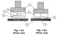
- Fig 1 (a) is a sectional view of a prior art pick and place assembly or tool holding a thin adhesive film 5 over a flat surface of a substrate 6.
- the pick and place tool generally comprises a collet or pickhead holder 1 and a suction head or vacuum collet 2. Inside the vacuum collet 2, there is a vacuum channel 3 for providing suction force to hold the adhesive film 5. Sometimes, there may be a recess 4 at the opening of the vacuum channel 3 to enhance the effectiveness of the suction force.
- the thin adhesive film 5 which may be in the form of a thermoplastic adhesive film, is held by the pick and place tool by suction means and vacuum suction is supplied through the vacuum channel 3 inside the collet 2.
- Fig. 1(b) is a sectional view of the prior art pick and place tool placing the thin adhesive film 5 onto the flat surface of the substrate 6.
- the adhesive film 5 is pasted onto the substate 6 and a compressive force is applied vertically downwards from the tool onto the adhesive film 5. This force should be high enough such that the pressure-sensitive adhesive film 5 can adhere onto the substrate 6.
- Tg glass transitional temperature
- thermoset epoxy curing temperature
- the recess 4 in the collet 2 is not desirable since it may contribute to the formation of voids 7. This is because air bubbles will be trapped inside the film 5 when the film (which is not totally flat) adheres onto the substrate 6 with a flat surface. These voids 7 are undesirable and will affect the reliability of the final product. Even a perfectly flat collet 2 without recess 4 cannot avoid the formation of these voids 7 along the adhesion interface since there is no way to apply pre-tension to the film 5 to flatten it, since the flim 5 is being held by vacuum suction only. To address this situation, a smaller opening for the vacuum channel 3 of the vacuum collet 2 can help to reduce the size of voids 7 that are created, but the solution can be further improved.
- Fig. 2(a) is a sectional view of a pick and place assembly or tool according to the preferred embodiment of the invention holding a film of material, such as a thin adhesive film 5, over a flat placement surface of a substrate 6.
- the suction head or vacuum collet 8 has a convex curvature for its contact surface 10, and does not have a recess.
- the contact surface 10 will contact the adhesive film 5 during pickup.
- the vacuum collet 8 of the pick and place tool is preferably deforamble so as to be compliant with the placement surface of the substrate 6 during placement of the film 5.
- the vacuum collet preferably includes a resilient material, such as silicone-based rubber or a stainless steel foil with a soft backing support.
- the material should be able to withstand temperatures of up to 200°C so that it works properly at the Tg of thermoplastic film (which is at approximately 150-180°C).
- the second requirement is that the contact surface should be of a type that an adhesive film 5 that it is holding does not tend to cling to it, especially under pressure and elevated temperature, to aid in removal of the pick and place tool after placement.
- the third requirement is that the hardness of the resilient material or the soft backing support should be in the range of 35-55 in Durometer, Shore "A" points at room temperature.
- a plurality of vacuum channels 9 having openings on the contact surface 10 are preferably distributed close to the corners of the vacuum collet 8 and none at the center of the collet 8.
- Small openings are used for the vacuum channels 9.
- Fig. 2(b) is a sectional view of the said pick and place tool according to the preferred embodiment placing the thin adhesive film 6 onto the flat surface of the substrate 6.
- the illustration shows that the adhesive film 5 will be flattened when a vertical downward compressive force is applied from the pick and place tool (comprising the holder 1 and vacuum collet 8) to push the adhesive film 5 against the flat surface of the substrate 6 (at an elevated temperature if necessary).
- the center portion of the convex contact surface 10 of the suction head or vacuum collet 8, as well as the corresponding portion of the adhesive film 5 adjacent to it, will contact the placement surface of the substrate 6 first. Then, since this convex contact surface 10 is made of resilient material, it will be deformed and flattened by the compressive force as the holder 1 moves downwards. In this way, any voids or air bubbles occurring between the adhesive film 5 and the surface of the substrate 6 will be gradually squeezed out of the film 5 outwards from the said portion of the film 5. A void-free attachment interface 11 between the adhesive film 5 and the substrate 6 may thereby be formed.
- the resilient convex profile of the suction head or vacuum collet 8 used as aforesaid for the application of thin thermoplastic adhesive films 5 can assist in providing void-fee attachment of these films 5 onto the flat surfaces of substrates 6 at elevated temperatures.
Landscapes
- Die Bonding (AREA)
- Container, Conveyance, Adherence, Positioning, Of Wafer (AREA)
- Photographic Developing Apparatuses (AREA)
Claims (12)
- Aufnahme- und Ablage-Anordnung zum Verbringen eines Films (5) aus Material zu einer Ablageoberfläche, wobei die Anordnung eine Einspanneinrichtung (8) mit einer im Wesentlichen konvexen Kontaktfläche (10) zum Kontaktieren des Films und eine Unterdruck-Saug-Vorrichtung umfasst, die auf der Kontaktfläche (10) Öffnungen aufweisende Unterdruckkanäle (9) enthält, wobei die Unterdruck-Saug-Vorrichtung dazu betrieben wird, eine Saugkraft zum Halten des Films zu erzeugen,
dadurch gekennzeichnet, dass
die Kontaktfläche (10) aus einem flexiblen Material hergestellt ist; und
die Kontaktfläche (10) dazu ausgelegt ist, durch die Ablageoberfläche bei Kontakt mit dieser während der Ablage des Films verformbar zu sein. - Aufnahme- und Ablage-Anordnung nach Anspruch 1, wobei die Kontaktfläche (10) ein flexibles Material aufweist.
- Aufnahme- und Ablage-Anordnung nach Anspruch 2, wobei das flexible Material dazu fähig ist, Temperaturen von bis zu 200 °C zu widerstehen.
- Aufnahme- und Ablage-Anordnung nach Anspruch 2 oder 3, wobei das flexible Material bei Raumtemperatur eine Härte im Bereich von 35 bis 55 Shore-A-Durometer-Punkten hat.
- Aufnahme- und Ablage-Anordnung nach einem der Ansprüche 2 bis 4, wobei das flexible Material einen auf Silikon basierenden Gummi umfasst.
- Aufnahme- und Ablage-Anordnung nach einem der Ansprüche 2 bis 5, wobei das flexible Material eine Edelstahlfolie mit einer weichen Hintergrund-Abstützung umfasst.
- Aufnahme- und Ablage-Anordnung zum Verbringen eines Films (5) aus Material zu einer Ablageoberfläche vorzugsweise nach einem der vorhergehenden Ansprüche, wobei die Anordnung eine Einspanneinrichtung (8) mit einer im Wesentlichen konvexen Kontaktfläche (10) zum Kontaktieren des Films und eine Unterdruck-Saug-Vorrichtung umfasst, die auf der Kontaktfläche (10) Öffnungen aufweisende Unterdruckkanäle (9) enthält, wobei die Unterdruck-Saug-Vorrichtung dazu betrieben wird, eine Saugkraft zum Halten des Films zu erzeugen,
dadurch gekennzeichnet, dass
die Unterdruckkanäle (9) nur in der Nähe der Ecken der Einspanneinrichtung (8) verteilt sind und in der Mitte der Einspanneinrichtung (8) abwesend sind. - Aufnahme- und Ablage-Anordnung nach Anspruch 7, wobei die Einspanneinrichtung (8) im Wesentlichen eine quadratische Form hat und vier Unterdruckkanäle (9) hat, von denen jeder in der Nähe einer Ecke der Einspanneinrichtung (8) angeordnet ist.
- Aufnahme- und Ablage-Anordnung nach einem der Ansprüche 7 bis 8, wobei die Breite jeder Öffnung kleiner als 0,5 mm ist.
- Aufnahme- und Ablage-Anordnung nach einem der vorhergehenden Ansprüche, wobei der Film aus Material ein thermoplastisches Klebeband oder ein mit Duroplast-Epoxidharz der Stufe B beschichteter Film ist.
- Verfahren zum Verbringen eines Films (5) aus Material unter der Verwendung der Aufnahme- und Ablage-Anordnung nach einem der vorhergehenden Ansprüche, wobei eine Material der Kontaktfläche der Einspanneinrichtung (8) so ausgewählt ist, dass der Film aus Material nicht die Tendenz hat, auf der Kontaktfläche (10) anzuhaften.
- Verfahren zum Verbringen eines Films (5) aus Material zu einer Ablageoberfläche eines Substrats unter der Verwendung einer Aufnahme- und Ablage-Anordnung nach einem der vorhergehenden Ansprüche, wobei ein mittlerer Teil des Films zuerst mit der Ablageoberfläche in Kontakt gebracht wird und dann die Einspanneinrichtung (8) weiter auf die Ablageoberfläche zu bewegt wird, um so die Kontaktfläche (10) zu verformen und flachzudrücken, um so jegliche eventuell zwischen dem Teil des Films und der Ablageoberfläche entstehende Hohlräume oder Luftblasen allmählich nach außen zu drücken.
Applications Claiming Priority (2)
| Application Number | Priority Date | Filing Date | Title |
|---|---|---|---|
| US452993 | 1982-12-27 | ||
| US10/452,993 US7182118B2 (en) | 2003-06-02 | 2003-06-02 | Pick and place assembly for transporting a film of material |
Publications (2)
| Publication Number | Publication Date |
|---|---|
| EP1489655A1 EP1489655A1 (de) | 2004-12-22 |
| EP1489655B1 true EP1489655B1 (de) | 2008-07-09 |
Family
ID=33418057
Family Applications (1)
| Application Number | Title | Priority Date | Filing Date |
|---|---|---|---|
| EP04076592A Expired - Lifetime EP1489655B1 (de) | 2003-06-02 | 2004-05-28 | Eine Aufnahme- und Ablagemontage um einen Film zu transportieren |
Country Status (4)
| Country | Link |
|---|---|
| US (1) | US7182118B2 (de) |
| EP (1) | EP1489655B1 (de) |
| AT (1) | ATE400893T1 (de) |
| DE (1) | DE602004014853D1 (de) |
Cited By (1)
| Publication number | Priority date | Publication date | Assignee | Title |
|---|---|---|---|---|
| DE102013220118A1 (de) | 2013-10-04 | 2015-04-23 | Robert Bosch Gmbh | Vorrichtung und Verfahren zum Transportieren zumindest eines folienartigen Bauteils |
Families Citing this family (18)
| Publication number | Priority date | Publication date | Assignee | Title |
|---|---|---|---|---|
| US20060003548A1 (en) * | 2004-06-30 | 2006-01-05 | Kobrinsky Mauro J | Highly compliant plate for wafer bonding |
| AT413385B (de) * | 2004-09-13 | 2006-02-15 | Amag Rolling Gmbh | Verfahren zum aufbringen einer schutzleiste auf ein kathodenblech zur elektrolytischen gewinnung eines metalls aus einer elektrolytflüssigkeit |
| CH697496B1 (de) * | 2005-12-23 | 2008-11-14 | Alphasem Gmbh | Werkzeug zum Aufnehmen, Absetzen oder Anpressen eines flächigen Objektes und Verwendung des Werkzeugs. |
| US7790507B2 (en) * | 2007-03-24 | 2010-09-07 | Texas Instruments Incorporated | Semiconductor die collet and method |
| TW200947641A (en) * | 2008-05-15 | 2009-11-16 | Gio Optoelectronics Corp | Die bonding apparatus |
| US20100024968A1 (en) * | 2008-07-30 | 2010-02-04 | United Technologies Corporation | Adhesive installation tool |
| US8092645B2 (en) * | 2010-02-05 | 2012-01-10 | Asm Assembly Automation Ltd | Control and monitoring system for thin die detachment and pick-up |
| US8432679B2 (en) | 2010-06-15 | 2013-04-30 | Apple Inc. | Silicone barrier for drive window |
| US8632363B2 (en) | 2010-08-31 | 2014-01-21 | Apple Inc. | Heat sealed connector assembly |
| DE102011013369A1 (de) * | 2010-12-30 | 2012-07-05 | Osram Opto Semiconductors Gmbh | Verfahren zum Herstellen einer Mehrzahl von Halbleiterbauelementen |
| JP2013033925A (ja) * | 2011-07-01 | 2013-02-14 | Tokyo Electron Ltd | 洗浄方法、プログラム、コンピュータ記憶媒体、洗浄装置及び剥離システム |
| US9079351B2 (en) * | 2012-06-22 | 2015-07-14 | Wisconsin Alumni Research Foundation | System for transfer of nanomembrane elements with improved preservation of spatial integrity |
| US10446728B2 (en) * | 2014-10-31 | 2019-10-15 | eLux, Inc. | Pick-and remove system and method for emissive display repair |
| DE102015224885B4 (de) | 2015-12-10 | 2024-11-07 | Adidas Ag | Verfahren für die Platzierung von Patches und hergestellte Artikel |
| TWI567011B (zh) * | 2016-06-15 | 2017-01-21 | 萬潤科技股份有限公司 | Method and device for conveying the components of the bonding process |
| CN118737998A (zh) * | 2017-03-02 | 2024-10-01 | Ev 集团 E·索尔纳有限责任公司 | 用于键合芯片的方法和装置 |
| GB2576774A (en) * | 2018-09-01 | 2020-03-04 | Vps Group Ltd | Apparatus for vehicle registration plate assembly |
| KR102724556B1 (ko) | 2019-06-04 | 2024-10-30 | 삼성전자주식회사 | 본딩 장치 및 그를 포함하는 반도체 패키지의 제조 설비 |
Family Cites Families (13)
| Publication number | Priority date | Publication date | Assignee | Title |
|---|---|---|---|---|
| JP2646121B2 (ja) * | 1988-09-29 | 1997-08-25 | 株式会社日立製作所 | 薄板部品用の真空吸着器、薄板部品の取扱方法、薄板部品取扱装置、半導体ウエハ移し替え装置 |
| GB8829196D0 (en) * | 1988-12-14 | 1989-01-25 | Du Pont Canada | Heat-sealing device for thermoplastic films |
| DE3912242A1 (de) * | 1989-04-14 | 1990-10-18 | Gurit Essex Ag | Vorrichtungen zum maschinellen aufbringen von flexiblen, einseitig klebbaren schichtkoerpern auf werkstuecke und verwendung derselben |
| US5405487A (en) * | 1992-06-30 | 1995-04-11 | Cms Gilbreth Packaging Systems, Inc. | Apparatus and method for applying labels onto small cylindrical articles and web and adhesive delivery mechanism |
| JPH06104300A (ja) | 1992-09-24 | 1994-04-15 | Fujitsu Ltd | ダイボンドテープ貼付けの装置及び方法 |
| JPH0766092A (ja) | 1993-08-23 | 1995-03-10 | Sumitomo Sitix Corp | 半導体ウエーハの接着方法および接着治具 |
| US5733410A (en) * | 1996-06-03 | 1998-03-31 | Motorola, Inc. | Labeling apparatus for applying labels with a rolling motion |
| US6248441B1 (en) * | 1999-03-24 | 2001-06-19 | Custom-Pak, Inc. | Method for enhancing the three-dimensional effect of a raised plastic surface using in-mold labeling and the label used therewith |
| KR100317648B1 (ko) | 1998-08-26 | 2002-02-19 | 윤종용 | 절연접착테이프에의하여다이접착되는반도체소자및다이접착방법그리고그장치 |
| JP3520820B2 (ja) | 1999-10-22 | 2004-04-19 | 松下電工株式会社 | 接着剤の転写方法 |
| JP2001334891A (ja) | 2000-05-24 | 2001-12-04 | Sumitomo Wiring Syst Ltd | 自動車用ドアヒンジ |
| JP2002334891A (ja) * | 2001-05-09 | 2002-11-22 | Canon Inc | 接着剤の転写ピンユニット及び転写方法 |
| TWI283906B (en) * | 2001-12-21 | 2007-07-11 | Esec Trading Sa | Pick-up tool for mounting semiconductor chips |
-
2003
- 2003-06-02 US US10/452,993 patent/US7182118B2/en not_active Expired - Lifetime
-
2004
- 2004-05-28 AT AT04076592T patent/ATE400893T1/de active
- 2004-05-28 EP EP04076592A patent/EP1489655B1/de not_active Expired - Lifetime
- 2004-05-28 DE DE602004014853T patent/DE602004014853D1/de not_active Expired - Lifetime
Cited By (1)
| Publication number | Priority date | Publication date | Assignee | Title |
|---|---|---|---|---|
| DE102013220118A1 (de) | 2013-10-04 | 2015-04-23 | Robert Bosch Gmbh | Vorrichtung und Verfahren zum Transportieren zumindest eines folienartigen Bauteils |
Also Published As
| Publication number | Publication date |
|---|---|
| US7182118B2 (en) | 2007-02-27 |
| EP1489655A1 (de) | 2004-12-22 |
| ATE400893T1 (de) | 2008-07-15 |
| DE602004014853D1 (de) | 2008-08-21 |
| US20040238112A1 (en) | 2004-12-02 |
Similar Documents
| Publication | Publication Date | Title |
|---|---|---|
| US7182118B2 (en) | Pick and place assembly for transporting a film of material | |
| CN101657890B (zh) | 带粘接剂芯片的制造方法 | |
| US7631680B2 (en) | Method of and mechanism for peeling adhesive tape bonded to segmented semiconductor wafer | |
| TW493236B (en) | Method for manufacturing semiconductor devices | |
| JP4261356B2 (ja) | 半導体パッケージを製造する方法 | |
| US7958628B2 (en) | Bonding tool for mounting semiconductor chips | |
| WO2011029890A1 (en) | Tool for picking a planar object from a supply station | |
| JP2010118373A (ja) | 半導体装置の製造方法 | |
| KR102101760B1 (ko) | 반도체 제조 장치, 반도체 장치의 제조 방법 및 콜릿 | |
| TWI719896B (zh) | 黏晶裝置,剝離單元,夾頭及半導體裝置的製造方法 | |
| CN114342050A (zh) | 半导体装置的制造方法及夹头 | |
| JP6542464B2 (ja) | 剥離装置 | |
| JP5431533B2 (ja) | 半導体装置の製造方法 | |
| TW501207B (en) | Power semiconductor die attach process using adhesive film | |
| JP2005252072A (ja) | 素子の実装方法及び搬送装置 | |
| JP4043720B2 (ja) | 半導体装置および半導体装置の製造方法 | |
| US7498202B2 (en) | Method for die attaching | |
| JP3580244B2 (ja) | 半導体装置および半導体装置の製造方法 | |
| CN100383929C (zh) | 一种半导体处理制程 | |
| JP3773427B2 (ja) | Bga型半導体装置の製造方法 | |
| JP2000133748A (ja) | 半導体パッケージ、その製造方法及び搬送フレーム | |
| KR20020058212A (ko) | 반도체 패키지용 다이 본딩장치의 히트 블록 구조 | |
| JP2002353401A (ja) | チップ吸着用ダイコレット及び半導体製造方法 | |
| JP2001332591A (ja) | 半導体装置の製造方法 | |
| JP2005353883A (ja) | 半導体装置の製造方法 |
Legal Events
| Date | Code | Title | Description |
|---|---|---|---|
| PUAI | Public reference made under article 153(3) epc to a published international application that has entered the european phase |
Free format text: ORIGINAL CODE: 0009012 |
|
| AK | Designated contracting states |
Kind code of ref document: A1 Designated state(s): AT BE BG CH CY CZ DE DK EE ES FI FR GB GR HU IE IT LI LU MC NL PL PT RO SE SI SK TR |
|
| AX | Request for extension of the european patent |
Extension state: AL HR LT LV MK |
|
| RIC1 | Information provided on ipc code assigned before grant |
Ipc: 7H 01L 21/58 A Ipc: 7H 01L 21/68 B Ipc: 7H 05K 13/04 B |
|
| 17P | Request for examination filed |
Effective date: 20050615 |
|
| AKX | Designation fees paid |
Designated state(s): AT DE GB NL SE |
|
| RAP1 | Party data changed (applicant data changed or rights of an application transferred) |
Owner name: ASM ASSEMBLY AUTOMATION LTD. |
|
| RIN1 | Information on inventor provided before grant (corrected) |
Inventor name: CHONG, CHI MING Inventor name: CHEUNG, YIU MING |
|
| 17Q | First examination report despatched |
Effective date: 20050901 |
|
| 17Q | First examination report despatched |
Effective date: 20050901 |
|
| 17Q | First examination report despatched |
Effective date: 20050901 |
|
| GRAP | Despatch of communication of intention to grant a patent |
Free format text: ORIGINAL CODE: EPIDOSNIGR1 |
|
| RIN1 | Information on inventor provided before grant (corrected) |
Inventor name: CHONG, CHI MING Inventor name: CHEUNG, YIU MING |
|
| GRAS | Grant fee paid |
Free format text: ORIGINAL CODE: EPIDOSNIGR3 |
|
| GRAA | (expected) grant |
Free format text: ORIGINAL CODE: 0009210 |
|
| AK | Designated contracting states |
Kind code of ref document: B1 Designated state(s): AT DE GB NL SE |
|
| REG | Reference to a national code |
Ref country code: GB Ref legal event code: FG4D |
|
| REF | Corresponds to: |
Ref document number: 602004014853 Country of ref document: DE Date of ref document: 20080821 Kind code of ref document: P |
|
| REG | Reference to a national code |
Ref country code: SE Ref legal event code: TRGR |
|
| PLBE | No opposition filed within time limit |
Free format text: ORIGINAL CODE: 0009261 |
|
| STAA | Information on the status of an ep patent application or granted ep patent |
Free format text: STATUS: NO OPPOSITION FILED WITHIN TIME LIMIT |
|
| 26N | No opposition filed |
Effective date: 20090414 |
|
| PGFP | Annual fee paid to national office [announced via postgrant information from national office to epo] |
Ref country code: NL Payment date: 20230417 Year of fee payment: 20 |
|
| PGFP | Annual fee paid to national office [announced via postgrant information from national office to epo] |
Ref country code: DE Payment date: 20230404 Year of fee payment: 20 |
|
| PGFP | Annual fee paid to national office [announced via postgrant information from national office to epo] |
Ref country code: SE Payment date: 20230412 Year of fee payment: 20 Ref country code: AT Payment date: 20230425 Year of fee payment: 20 |
|
| PGFP | Annual fee paid to national office [announced via postgrant information from national office to epo] |
Ref country code: GB Payment date: 20230406 Year of fee payment: 20 |
|
| REG | Reference to a national code |
Ref country code: DE Ref legal event code: R071 Ref document number: 602004014853 Country of ref document: DE |
|
| REG | Reference to a national code |
Ref country code: NL Ref legal event code: MK Effective date: 20240527 |
|
| REG | Reference to a national code |
Ref country code: GB Ref legal event code: PE20 Expiry date: 20240527 |
|
| REG | Reference to a national code |
Ref country code: SE Ref legal event code: EUG |
|
| PG25 | Lapsed in a contracting state [announced via postgrant information from national office to epo] |
Ref country code: GB Free format text: LAPSE BECAUSE OF EXPIRATION OF PROTECTION Effective date: 20240527 |
|
| REG | Reference to a national code |
Ref country code: AT Ref legal event code: MK07 Ref document number: 400893 Country of ref document: AT Kind code of ref document: T Effective date: 20240528 |
|
| PG25 | Lapsed in a contracting state [announced via postgrant information from national office to epo] |
Ref country code: GB Free format text: LAPSE BECAUSE OF EXPIRATION OF PROTECTION Effective date: 20240527 |