EP1484949B1 - Verarbeiten von Materialien mit niedriger Dielektrizitätskonstante für die Hochgeschwindigkeitselektronik - Google Patents
Verarbeiten von Materialien mit niedriger Dielektrizitätskonstante für die Hochgeschwindigkeitselektronik Download PDFInfo
- Publication number
- EP1484949B1 EP1484949B1 EP04020818A EP04020818A EP1484949B1 EP 1484949 B1 EP1484949 B1 EP 1484949B1 EP 04020818 A EP04020818 A EP 04020818A EP 04020818 A EP04020818 A EP 04020818A EP 1484949 B1 EP1484949 B1 EP 1484949B1
- Authority
- EP
- European Patent Office
- Prior art keywords
- dielectric constant
- porous
- low dielectric
- materials
- porous layer
- Prior art date
- Legal status (The legal status is an assumption and is not a legal conclusion. Google has not performed a legal analysis and makes no representation as to the accuracy of the status listed.)
- Expired - Lifetime
Links
Images


Classifications
-
- H—ELECTRICITY
- H05—ELECTRIC TECHNIQUES NOT OTHERWISE PROVIDED FOR
- H05K—PRINTED CIRCUITS; CASINGS OR CONSTRUCTIONAL DETAILS OF ELECTRIC APPARATUS; MANUFACTURE OF ASSEMBLAGES OF ELECTRICAL COMPONENTS
- H05K1/00—Printed circuits
- H05K1/02—Details
- H05K1/03—Use of materials for the substrate
- H05K1/0313—Organic insulating material
-
- H—ELECTRICITY
- H05—ELECTRIC TECHNIQUES NOT OTHERWISE PROVIDED FOR
- H05K—PRINTED CIRCUITS; CASINGS OR CONSTRUCTIONAL DETAILS OF ELECTRIC APPARATUS; MANUFACTURE OF ASSEMBLAGES OF ELECTRICAL COMPONENTS
- H05K1/00—Printed circuits
- H05K1/02—Details
- H05K1/0213—Electrical arrangements not otherwise provided for
- H05K1/0237—High frequency adaptations
- H05K1/024—Dielectric details, e.g. changing the dielectric material around a transmission line
-
- H—ELECTRICITY
- H05—ELECTRIC TECHNIQUES NOT OTHERWISE PROVIDED FOR
- H05K—PRINTED CIRCUITS; CASINGS OR CONSTRUCTIONAL DETAILS OF ELECTRIC APPARATUS; MANUFACTURE OF ASSEMBLAGES OF ELECTRICAL COMPONENTS
- H05K1/00—Printed circuits
- H05K1/02—Details
- H05K1/03—Use of materials for the substrate
- H05K1/0313—Organic insulating material
- H05K1/0353—Organic insulating material consisting of two or more materials, e.g. two or more polymers, polymer + filler, + reinforcement
- H05K1/0373—Organic insulating material consisting of two or more materials, e.g. two or more polymers, polymer + filler, + reinforcement containing additives, e.g. fillers
-
- H—ELECTRICITY
- H05—ELECTRIC TECHNIQUES NOT OTHERWISE PROVIDED FOR
- H05K—PRINTED CIRCUITS; CASINGS OR CONSTRUCTIONAL DETAILS OF ELECTRIC APPARATUS; MANUFACTURE OF ASSEMBLAGES OF ELECTRICAL COMPONENTS
- H05K3/00—Apparatus or processes for manufacturing printed circuits
- H05K3/0011—Working of insulating substrates or insulating layers
- H05K3/0017—Etching of the substrate by chemical or physical means
- H05K3/0026—Etching of the substrate by chemical or physical means by laser ablation
- H05K3/0032—Etching of the substrate by chemical or physical means by laser ablation of organic insulating material
-
- H10W70/093—
-
- H10W70/614—
-
- H10W70/69—
-
- H10W99/00—
-
- H—ELECTRICITY
- H05—ELECTRIC TECHNIQUES NOT OTHERWISE PROVIDED FOR
- H05K—PRINTED CIRCUITS; CASINGS OR CONSTRUCTIONAL DETAILS OF ELECTRIC APPARATUS; MANUFACTURE OF ASSEMBLAGES OF ELECTRICAL COMPONENTS
- H05K2201/00—Indexing scheme relating to printed circuits covered by H05K1/00
- H05K2201/01—Dielectrics
- H05K2201/0104—Properties and characteristics in general
- H05K2201/0116—Porous, e.g. foam
-
- H—ELECTRICITY
- H05—ELECTRIC TECHNIQUES NOT OTHERWISE PROVIDED FOR
- H05K—PRINTED CIRCUITS; CASINGS OR CONSTRUCTIONAL DETAILS OF ELECTRIC APPARATUS; MANUFACTURE OF ASSEMBLAGES OF ELECTRICAL COMPONENTS
- H05K2201/00—Indexing scheme relating to printed circuits covered by H05K1/00
- H05K2201/01—Dielectrics
- H05K2201/0137—Materials
- H05K2201/015—Fluoropolymer, e.g. polytetrafluoroethylene [PTFE]
-
- H—ELECTRICITY
- H05—ELECTRIC TECHNIQUES NOT OTHERWISE PROVIDED FOR
- H05K—PRINTED CIRCUITS; CASINGS OR CONSTRUCTIONAL DETAILS OF ELECTRIC APPARATUS; MANUFACTURE OF ASSEMBLAGES OF ELECTRICAL COMPONENTS
- H05K2201/00—Indexing scheme relating to printed circuits covered by H05K1/00
- H05K2201/01—Dielectrics
- H05K2201/0137—Materials
- H05K2201/0158—Polyalkene or polyolefin, e.g. polyethylene [PE], polypropylene [PP]
-
- H—ELECTRICITY
- H05—ELECTRIC TECHNIQUES NOT OTHERWISE PROVIDED FOR
- H05K—PRINTED CIRCUITS; CASINGS OR CONSTRUCTIONAL DETAILS OF ELECTRIC APPARATUS; MANUFACTURE OF ASSEMBLAGES OF ELECTRICAL COMPONENTS
- H05K2203/00—Indexing scheme relating to apparatus or processes for manufacturing printed circuits covered by H05K3/00
- H05K2203/08—Treatments involving gases
- H05K2203/083—Evaporation or sublimation of a compound, e.g. gas bubble generating agent
-
- H—ELECTRICITY
- H05—ELECTRIC TECHNIQUES NOT OTHERWISE PROVIDED FOR
- H05K—PRINTED CIRCUITS; CASINGS OR CONSTRUCTIONAL DETAILS OF ELECTRIC APPARATUS; MANUFACTURE OF ASSEMBLAGES OF ELECTRICAL COMPONENTS
- H05K2203/00—Indexing scheme relating to apparatus or processes for manufacturing printed circuits covered by H05K3/00
- H05K2203/12—Using specific substances
- H05K2203/122—Organic non-polymeric compounds, e.g. oil, wax or thiol
-
- H—ELECTRICITY
- H05—ELECTRIC TECHNIQUES NOT OTHERWISE PROVIDED FOR
- H05K—PRINTED CIRCUITS; CASINGS OR CONSTRUCTIONAL DETAILS OF ELECTRIC APPARATUS; MANUFACTURE OF ASSEMBLAGES OF ELECTRICAL COMPONENTS
- H05K3/00—Apparatus or processes for manufacturing printed circuits
- H05K3/38—Improvement of the adhesion between the insulating substrate and the metal
- H05K3/386—Improvement of the adhesion between the insulating substrate and the metal by the use of an organic polymeric bonding layer, e.g. adhesive
-
- H10W70/099—
-
- H10W70/60—
-
- H10W70/682—
-
- H10W72/073—
-
- H10W72/874—
-
- H10W90/00—
-
- H10W90/734—
-
- Y—GENERAL TAGGING OF NEW TECHNOLOGICAL DEVELOPMENTS; GENERAL TAGGING OF CROSS-SECTIONAL TECHNOLOGIES SPANNING OVER SEVERAL SECTIONS OF THE IPC; TECHNICAL SUBJECTS COVERED BY FORMER USPC CROSS-REFERENCE ART COLLECTIONS [XRACs] AND DIGESTS
- Y10—TECHNICAL SUBJECTS COVERED BY FORMER USPC
- Y10S—TECHNICAL SUBJECTS COVERED BY FORMER USPC CROSS-REFERENCE ART COLLECTIONS [XRACs] AND DIGESTS
- Y10S521/00—Synthetic resins or natural rubbers -- part of the class 520 series
- Y10S521/918—Physical aftertreatment of a cellular product
-
- Y—GENERAL TAGGING OF NEW TECHNOLOGICAL DEVELOPMENTS; GENERAL TAGGING OF CROSS-SECTIONAL TECHNOLOGIES SPANNING OVER SEVERAL SECTIONS OF THE IPC; TECHNICAL SUBJECTS COVERED BY FORMER USPC CROSS-REFERENCE ART COLLECTIONS [XRACs] AND DIGESTS
- Y10—TECHNICAL SUBJECTS COVERED BY FORMER USPC
- Y10T—TECHNICAL SUBJECTS COVERED BY FORMER US CLASSIFICATION
- Y10T29/00—Metal working
- Y10T29/49—Method of mechanical manufacture
- Y10T29/49002—Electrical device making
- Y10T29/49117—Conductor or circuit manufacturing
- Y10T29/49124—On flat or curved insulated base, e.g., printed circuit, etc.
- Y10T29/49155—Manufacturing circuit on or in base
Definitions
- This invention relates generally to low dielectric constant porous materials and, more particularly, to a process for using porous layers in printed circuit boards and over electronic circuits and supporting substrates.
- Porous polytetrafluoroethylene (PTFE) materials such as GortexTM (Gortex is a trademark of W.L. Gore & Associates, Inc., of Newark, DE) have excellent low dielectric constant properties, but unfortunately they absorb process chemicals in their pores during MCM (multichip module) or PC (printed circuit) board processing that cannot be removed. Additionally, the fact that the porous material deforms during pressurized processing destroys its porous properties, and therefore the deformed material does not provide the desired consistent low dielectric constant.
- the DuPont Teflon polytetrafluoroethylene line of materials has intrinsically low dielectric constants and has the necessary high temperature stability for most industrial and military uses.
- Gortex material is a Teflon PTFE-based material that is filled with micro-pores that create a foam-like cloth material.
- Porous PTFE material is generally used in clothes to simultaneously provide warmth and allow perspiration and moisture vapors to vent through its pores.
- Porous PTFE material is alternatively sold as a filled porous PTFE material.
- Unfilled porous PTFE material is an excellent candidate for high frequency circuits because the dielectric constant can be significantly less than that found in other materials.
- the pores can collapse under pressure and/or be filled with processing materials during fabrication which cannot be easily removed.
- Ceramic foam materials are discussed, for example, in “ Giants in advanced ceramics,” Ceramic Industry, vol. 141, 47 (March 1993 ), and Te-Kao Wu, "Dielectric properties measurement of substrate and support materials,” Microwave and Optical Technology Letters, vol. 3, 283-286 (March 1990 ). These materials, however, are inflexible and not fabricated in large area sections. Because the ceramic foam materials are inflexible, they can be used as substrates but cannot be used in overlay technologies that are not perfectly flat. Because ceramic foam materials are fragile, they are typically not capable of withstanding PC board lamination processing in their intrinsic state. Furthermore, ceramic foam materials can be filled with processing materials which degrade their low dielectric constant.
- porous PTFE material and ceramic foam material
- the metal tends to extend into the pores and it is thus difficult to achieve a smooth and continuous metal surface for use in high frequency applications where skin-effect related losses are of importance.
- Polymer materials in high frequency circuits are preferably laser ablatable by ultraviolet light in order to form the via openings through which different layers of metallization are connected.
- Laser processing is normally done with several passes of the laser beam with a power ranging from 0.5 to 2.0 watts, with a preferred maximum power level being about 1.5 watts.
- a dielectric layer is characterized as being laser ablatable, it means that such layer can be totally removed by progressive passes of a laser beam of this power level, and when it is characterized as not being laser ablatable, it means that a layer is not completely removed by progressive passes of such a laser beam.
- One method of adaptive laser ablation is discussed in Eichelberger et al., U.S.
- Patent No. 4,835,704 Most polytetrafluoroethylene materials are not laser ablatable and generally do not easily adhere to other materials. A method of modifying the ultraviolet absorption characteristics of a polymer material with the addition of an ultraviolet absorbing dye is discussed is Cole et al., U.S. Patent No. 5,169,678 .
- preferred materials are those which can be processed at a laser frequency of 351 nm.
- This frequency was selected in accordance with the characteristics of desirable dielectric layers such as KaptonTM polyimide (Kapton is a trademark of E.I. DuPont de Nemours and Co.) and the fact that there are commercial photoresists which can be processed at this frequency.
- UltemTM polyetherimide resin Ultem is a registered trademark of General Electric Co.
- the Ultem polyetherimide resin is laser ablatable at 351 nm.
- PC boards typically have dielectric constants ranging from 2 through 5, and nonporous ceramics can have dielectric constants as high as 9. It would be desirable to have a low dielectric constant PC board material for use in high frequency and high speed electronics.
- the present invention aims to provide a new material and method of manufacturing high frequency and high speed electronic circuits with low power capabilities.
- This invention also aims to provide a method for processing low dielectric constant porous materials which does not leave process chemicals behind in the porous materials.
- a method for adding materials to the pores of the porous material that allow laser processing at an ultra-violet (UV) wavelength of about 350 nanometers (nm).
- UV ultra-violet
- This invention may also provide low dielectric constant polymer and ceramic PC boards.
- This invention modifies a low dielectric constant polymeric porous material, such as porous PTFE material, which has a dielectric constant of approximately 1.2-1.3, by filling the material's pores with a sublimable (or otherwise removable) material that prevents deformation and enables laser processing during high speed circuit fabrication.
- the term "low dielectric constant” is intended to mean a dielectric constant as close to 1 as possible and not greater than about 2. After processing, the filler material is removed, and the original porous material is left with the intrinsically low dielectric constant.
- the process which enables foam-like materials to be laminated and laser machined without the use of solvents or other chemical processing, can be used in PC boards, MCM modules, and anywhere else low dielectric constant surfaces are desired.
- Porous PTFE material is approximately 70% air and is generally made by stretching PTFE to cause approximately nine billion holes per square inch to be distributed evenly throughout its volume.
- This porous structure is composed of mostly air and can readily be filled with a sublimable material.
- the resulting porous material can be used as a low dielectric constant material in the manufacture of high frequency circuits and can reduce the need for laser ablation of material situated over air bridge structures and other microwave structures and devices.
- a method for applying and ablating a low dielectric constant material over a substrate comprises attaching a low dielectric constant porous polymer layer having a dielectric constant no greater than 2 to a surface of the substrate; applying mask material over the polymer layer; forming a via in the mask material extending through to the polymer layer; diffusing an additive material in a region of the polymer layer through the via in the mask material; removing the mask material; and ablating at least some of the polymer layer in the region where the additive material was diffused.
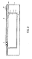
- FIGs. 1-5 are views showing steps in a process for applying a low dielectric constant porous material over a selected surface.
- a semiconductor chip 14 which for example may comprise a GaAs (gallium arsenide) chip having chip pads 16, is attached with an adhesive 12 in a chip well 18 of a milled substrate 10.
- the substrate may comprise any suitable structural material such as, for example, aluminum nitride or beryllium oxide.
- Adhesive 12 may comprise a material such as Ultem polyetherimide resin or silicone epoxy which can withstand high temperature processing.
- a low dielectric constant porous layer 20 is applied over the surfaces of substrate 10 and chip 14.
- the porous layer comprises a porous PTFE material having its pores filled with an additive material.
- the pores have diameters ranging approximately from 0.01 to 5 ⁇ m.
- the porous material is a polymer material. Expanded PTFE is a useful porous layer because it does not dissolve in most of the fabricating chemicals. Other examples of potentially useful porous material include polyethylene and polystyrene, for example.
- the selected additive material must be capable of withstanding high processing temperatures and capable of removal after processing by any appropriate process, such as heat or a combination of heat and applied vacuum.
- the additive material may comprise materials such as low melting temperature waxes, anthraquinone (as well as derivatives of anthraquinone such as alizarin), and other sublimable organic solids, such as adipic and other dicarboxylic acids. Some of these additive materials may require vacuum and heat combinations to sublime, whereas others tend to diffuse or evaporate from the material. A short list of sublimable materials can be found in the Handbook of Chemistry and Physics, 60th Ed. pages C-722-723. Many of the listed materials can be readily used with this invention. A combination of several additive materials may be desirable to provide a removable material which can absorb appropriate wavelengths for laser ablation.
- Porous layer 20 is heated to the softening point under pressure and attached to the substrate surface to achieve a bonded laminate.
- the pressure and temperature parameters are chosen so that the additive material does not significantly sublime, diffuse, or evaporate during the attachment.
- the outer porous layer surface can have another coating of the additive material added to refresh the surface after lamination.
- Either an adaptive laser, such as described in aforementioned Eichelberger et al., U.S. Pat. No. 4,835,704 , or a mask process is then used to form via openings 24 over selected chip pads 16, as shown in FIG. 3 .
- layers such as porous PTFE are not typically laser ablatable using the preferred wavelengths, the process of filling the pores of porous layer 20 with additive material causes the porous layer to be laser ablatable, as further discussed below.
- a layer of electrically conductive material is applied over porous layer 20 and patterned to form a pattern of electrical conductors 22 which, in a preferred embodiment, includes a bonding pad 26.
- the pattern of electrical conductors comprises a buffer layer of metallization such as titanium or chromium covered by a layer of copper which in turn is covered by a second buffer layer. These metals can be patterned with standard photoresist techniques, as discussed in Eichelberger et al., U.S. 4,783,695 .
- FIG. 5 is a sectional side view similar to that of FIG. 3 .
- FIG. 4 is an enlarged sectional side view along line 4-4' of FIG. 5 .
- Substrate 10 can be heated (either with or without vacuum conditions, depending on the additive material) to sublime, diffuse, or evaporate the additive material. Because the additive material does not sublime directly through the pattern of electrical conductors 22, additive material under the pattern of electrical conductors has a longer release path 21 a as compared with the release path 21 b of additive material not under the pattern of electrical conductors. The longer release path may require a longer heating period.
- Dye molecules such as anthraquinone or alizarin are relatively small molecules and fit between the spaces of the coiled polymer chains which preferably make up the porous layer. When heated above the sublimation temperature, the individual dye molecules, in the gas phase, will vent or pass through these spaces and be released from the porous layer.
- the metal does not significantly protrude into the porous layer and thus has a smooth surface as required for low loss high frequency applications.
- UV ultraviolet
- UV light acts to scission the material and thus create smaller molecules which can move easily and pass out of the porous materials.
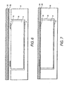
- FIGs. 6-9 are views showing steps in a process for applying a low dielectric constant porous layer similar to the process steps shown in FIGs. 1-5 with the addition of an amorphous adhesive 28 having a low dielectric constant, such as available from DuPont under the name AF 1600 or 2400 Teflon polytetrafluoroethylene, that maintains excellent adhesion to the porous layer after the additive material is removed.
- an amorphous adhesive 28 having a low dielectric constant such as available from DuPont under the name AF 1600 or 2400 Teflon polytetrafluoroethylene, that maintains excellent adhesion to the porous layer after the additive material is removed.
- Another potentially useful adhesive with a low dielectric constant is polyphenylene oxide.
- These low dielectric adhesives are preferably doped with an ultraviolet light absorbing dye as discussed in aforementioned Cole et al., U.S. Patent No. 5,169,678 .
- porous layer 20 is immersed and soaked in the additive material which is dissolved in a solvent. Ion implantation, pressure, or a combination of pressure and heat can be used to Increase the permeation of the additive material throughout the porous layer.
- adhesive 28 is either applied to porous layer 20 or applied to the substrate surface directly. It is helpful to position the additive material in the pores of the porous layer prior to the application and lamination of the porous layer to the substrate surface to prevent the adhesive from wicking or protruding into the pores. Thus the removal of the additive material from the porous layer can be accomplished while maintaining sufficient adhesion of the porous layer to the surface.
- FIGs. 7-9 illustrate views of process steps similar to those of FIGs. 2 , 3 , and 5 , respectively, but do not require as much heat to obtain adhesion of the porous layer to the desired surface.
- AF Teflon polytetrafluoroethylene is used as an adhesive
- the porous layer can attain adequate adhesion to substrate and chip surfaces in the temperature range of 225 °C - 250 °C.
- the step of forming a via opening 24 through porous layer 20 includes forming a corresponding via through adhesive 28.
- the addition of the thin adhesive 28 increases the dielectric constant above the surface because dielectric constants generally act in series and are proportional to the relative thicknesses of the adjacent materials. When the porous layer is much thicker than the adhesive, however, the dielectric constant can approach that of the porous layer and be suitably low.
- FIGs. 10-11 are views showing steps in a process for applying multiple low dielectric constant porous layers.
- a second additive filled porous layer 30 is applied with a second adhesive 32 to the outer surface of porous layer 20a of the structure shown in FIG. 9 .
- the second porous layer and all subsequent layers can be processed as described with respect to FIGs. 7-9 above by forming a via opening 34 extending to a portion of the pattern of electrical conductors 22, applying a second pattern of electrical conductors 36, and removing the additive material to result in the structure shown in FIG. 11 .
- the second adhesive is thin and therefore does not fill the lower vias 24, thus providing an air dielectric constant (about 1) in the metallized via areas.
- the porous layers and adhesives all comprise polytetrafluoroethylene.
- This embodiment uses two different DuPont AF Teflon polytetrafluoroethylene materials such as AF 1600 for adhesives 28 and 32 and AF 2400 for porous layers 20 and 30. These two materials have sufficiently different melting points so that when AF 2400 is a solid the AF 1600 can melt and function as a bonding glue.
- AF Teflon polytetrafluoroethylene materials can have various sublimable materials added that will enable 248-365 nm laser ablation and that can be subsequently be removed by heat or heat and vacuum conditions.
- additive materials include the above-discussed low melting temperature waxes, anthraquinone and its derivatives, and other sublimable organic solids.
- additive materials enables a material that is optically transparent to approximately 200 nm to be laser processable at more conventional laser frequencies such as pulsed excimer lasers at frequencies of 248 nm, 266 nm, 308 nm, and 351 nm, and ion argon or krypton lasers at frequencies of at 350-365 nm and 325 nm, respectively, and subsequently be removed.
- pulsed excimer lasers at frequencies of 248 nm, 266 nm, 308 nm, and 351 nm
- ion argon or krypton lasers at frequencies of at 350-365 nm and 325 nm, respectively, and subsequently be removed.
- the AF Teflon polytetrafluoroethylene layers will release the additive material easily because the materials can be heated near the Tg (glass transition temperature) where the additive material is passed by permeation through the softened material with ease. This process is time, thickness, temperature, and pressure dependent.
- An AF 2400 Teflon polytetrafluoroethylene porous layer can be film cast onto a release plate and an AF 1600 Teflon polytetrafluoroethylene adhesive material can be applied over the top of the porous layer without cracking it, enabling a composite structure that can then be laminated to a PC board or MCM structure.
- This embodiment can be used to reduce the impedance loading which occurs when using high dielectric constant materials.
- Some circuit chip manufacturers employ air bridges to obtain low impedance loading on critical areas of GaAs microcircuits. Typically, when these chips are situated in an integrated circuit, any overlying and underlying material must be removed in the area of the air bridges for optimal performance. This invention may reduce the need to remove material and thus enable new chip interconnection structures to be fabricated.
- FIGs. 12-16 are views showing steps in a doping process for enabling laser ablation of low dielectric constant porous layer 40 according to the invention.
- the porous layer is first applied to a substrate 10 surface, as discussed with respect to FIG. 2 , but without the additive material.
- a laser ablatable mask material 42 such as Kapton polyimide for example, is deposited over the outer surface of the porous layer.
- a via opening 46 over a portion of an electrical conductor 44 is formed in the mask material revealing the porous layer, as shown in FIG. 12 .
- the via is preferably formed with an argon laser, but can also be formed using other conventional methods such as plasma or reactive ion etching, for example.
- the additive material can be supplied to porous layer 40 in a pressure vessel 50 through a pressure port 52 using a heat source 54.
- the dopant may comprise a light absorbing dye such as discussed in aforementioned Cole et al., U.S. Patent No. 5,169,678 .
- Mask material 42 limits doping or diffusion to the localized areas 48 where the vias have been formed to cause permeation of the of the additive material for enabling laser ablation at CW argon ion laser frequencies. If desired, mask material 42 can also be applied over the side edges of the porous layer to prevent doping of the side edges. Slight doping which may occur along the edges of the porous layer, however, does not present any problems.
- FIG. 14 illustrates a doped region ready for laser processing.
- the mask material can be removed, as shown in FIG. 15 , and a laser can be used to produce vias in the porous layer where the additive material was doped because of the selective absorption of the excimer laser energy in the doped via areas.
- any remaining dopant material can be removed by a process such as sublimation, for example, leaving the material again transparent to the excimer laser's light energy, as shown by via 56 in FIG. 16 .
- FIGs. 17-19 are views showing steps in a process for forming a low dielectric constant printed circuit board.
- a porous layer 110 is filled with additive material as described with respect to FIG. 2 .
- the porous layer is preferably coated on both sides with thin layers of an adhesive material 112a and 112b, comprising a material such as AF 1600 or 2400 Teflon polytetrafluoroethylene, which in turn are coated with respective layers of metallization 114a and 114b, comprising a material such as copper, as shown in FIG. 17 .
- DuPont FEP or PFA Teflon polytetrafluoroethylene is applied with a pinch roll laminator such as used in PC board processing.
- holes 116 are punched or drilled through the porous material, adhesive, and metallization, and, as shown in FIG. 19 , the layers of metallization are patterned to form metallization lines on the board.
- the patterning is performed using a layer of photoresist (not shown) which is removed after patterning. If desired, any adhesive left exposed after the patterning of the metallization layer can be removed by RIE (reactive ion etching).
- RIE reactive ion etching
Landscapes
- Engineering & Computer Science (AREA)
- Microelectronics & Electronic Packaging (AREA)
- Physics & Mathematics (AREA)
- Optics & Photonics (AREA)
- Manufacturing & Machinery (AREA)
- Laminated Bodies (AREA)
- Manufacturing Of Printed Wiring (AREA)
- Production Of Multi-Layered Print Wiring Board (AREA)
- Printing Elements For Providing Electric Connections Between Printed Circuits (AREA)
Claims (5)
- Verfahren zum Aufbringen und Abtragen eines Materials mit niedriger dielektrischer Konstante auf ein bzw. von einem Substrat (10, 14), umfassend die Schritte:Anlagern einer porösen Polymerschicht (20) mit niedriger dielektrischer Konstante mit einer dielektrischen Konstante von nicht größer als 2 auf eine Oberfläche des Substrats;Aufbringen eines Maskenmaterials auf die Polymerschicht;Bilden einer Lücke (24) in dem Maskenmaterial, die sich hindurch bis zur Polymerschicht erstreckt;Diffundieren eines Zusatzmaterials in einen Bereich der Polymerschicht durch die Lücke im Maskenmaterial;Entfernen des Maskenmaterials; undAbtragen zumindest eines Teils der Polymerschicht in der Region, in welcher das Zusatzmaterial diffundiert wurde.
- Verfahren nach Anspruch 1, ferner einschließend den Endschritt des Entfernens von jeglichem restlichem Zusatzmaterial von der Polymerschicht durch Sublimation.
- Verfahren nach Anspruch 2, wobei die Polymerschicht ein Polytetrafluorethylen und das Maskenmaterial ein Polyimid umfasst.
- Verfahren nach Anspruch 1, wobei die poröse Schicht ein Material umfasst, ausgewählt aus der Gruppe, bestehend aus Polytetrafluorethylen, Polyethylen und Polystyrol.
- Verfahren nach Anspruch 4, wobei das Zusatzmaterial ein Material umfasst, ausgewählt aus der Gruppe, bestehend aus Wachs, Anthrachinon und sublimierbaren organischen Feststoffen.
Applications Claiming Priority (3)
| Application Number | Priority Date | Filing Date | Title |
|---|---|---|---|
| US08/247,820 US5449427A (en) | 1994-05-23 | 1994-05-23 | Processing low dielectric constant materials for high speed electronics |
| US247820 | 1994-05-23 | ||
| EP95920427A EP0710430B1 (de) | 1994-05-23 | 1995-05-15 | Verarbeiten von materialien mit niedriger dieelektrizitätskonstante für die hochgeschwindigkeitselektronik |
Related Parent Applications (1)
| Application Number | Title | Priority Date | Filing Date |
|---|---|---|---|
| EP95920427A Division EP0710430B1 (de) | 1994-05-23 | 1995-05-15 | Verarbeiten von materialien mit niedriger dieelektrizitätskonstante für die hochgeschwindigkeitselektronik |
Publications (3)
| Publication Number | Publication Date |
|---|---|
| EP1484949A2 EP1484949A2 (de) | 2004-12-08 |
| EP1484949A3 EP1484949A3 (de) | 2004-12-15 |
| EP1484949B1 true EP1484949B1 (de) | 2009-05-06 |
Family
ID=22936514
Family Applications (2)
| Application Number | Title | Priority Date | Filing Date |
|---|---|---|---|
| EP95920427A Expired - Lifetime EP0710430B1 (de) | 1994-05-23 | 1995-05-15 | Verarbeiten von materialien mit niedriger dieelektrizitätskonstante für die hochgeschwindigkeitselektronik |
| EP04020818A Expired - Lifetime EP1484949B1 (de) | 1994-05-23 | 1995-05-15 | Verarbeiten von Materialien mit niedriger Dielektrizitätskonstante für die Hochgeschwindigkeitselektronik |
Family Applications Before (1)
| Application Number | Title | Priority Date | Filing Date |
|---|---|---|---|
| EP95920427A Expired - Lifetime EP0710430B1 (de) | 1994-05-23 | 1995-05-15 | Verarbeiten von materialien mit niedriger dieelektrizitätskonstante für die hochgeschwindigkeitselektronik |
Country Status (6)
| Country | Link |
|---|---|
| US (3) | US5449427A (de) |
| EP (2) | EP0710430B1 (de) |
| JP (2) | JP3769297B2 (de) |
| CA (1) | CA2163627A1 (de) |
| DE (2) | DE69533789T2 (de) |
| WO (1) | WO1995032604A1 (de) |
Families Citing this family (70)
| Publication number | Priority date | Publication date | Assignee | Title |
|---|---|---|---|---|
| US5785787A (en) * | 1994-05-23 | 1998-07-28 | General Electric Company | Processing low dielectric constant materials for high speed electronics |
| US5889104A (en) * | 1996-01-11 | 1999-03-30 | W. L. Gore & Associates, Inc. | Low dielectric constant material for use as an insulation element in an electronic device |
| GB9610689D0 (en) * | 1996-05-22 | 1996-07-31 | Int Computers Ltd | Flip chip attachment |
| JP3305211B2 (ja) | 1996-09-10 | 2002-07-22 | 松下電器産業株式会社 | 半導体装置及びその製造方法 |
| US5900674A (en) | 1996-12-23 | 1999-05-04 | General Electric Company | Interface structures for electronic devices |
| US5938452A (en) * | 1996-12-23 | 1999-08-17 | General Electric Company | Flexible interface structures for electronic devices |
| US6303488B1 (en) | 1997-02-12 | 2001-10-16 | Micron Technology, Inc. | Semiconductor processing methods of forming openings to devices and substrates, exposing material from which photoresist cannot be substantially selectively removed |
| JP2002513512A (ja) * | 1997-04-03 | 2002-05-08 | ダブリュ.エル.ゴア アンド アソシエーツ,インコーポレイティド | 改良された絶縁耐力を備えた低誘電率材料 |
| US6077792A (en) * | 1997-07-14 | 2000-06-20 | Micron Technology, Inc. | Method of forming foamed polymeric material for an integrated circuit |
| SE510487C2 (sv) * | 1997-09-17 | 1999-05-31 | Ericsson Telefon Ab L M | Flerlagerskretskort |
| JP3661444B2 (ja) * | 1998-10-28 | 2005-06-15 | 株式会社ルネサステクノロジ | 半導体装置、半導体ウエハ、半導体モジュールおよび半導体装置の製造方法 |
| JP2002530505A (ja) | 1998-11-24 | 2002-09-17 | ザ ダウ ケミカル カンパニー | 架橋性マトリックス前駆体および気孔発生体を含有する組成物、並びにそれから製造された多孔質マトリックス |
| US6495468B2 (en) | 1998-12-22 | 2002-12-17 | Micron Technology, Inc. | Laser ablative removal of photoresist |
| WO2000044210A1 (en) * | 1999-01-22 | 2000-07-27 | Spectrian Corporation | Multi-layer rf printed circuit architecture |
| US7276788B1 (en) | 1999-08-25 | 2007-10-02 | Micron Technology, Inc. | Hydrophobic foamed insulators for high density circuits |
| US6413827B2 (en) | 2000-02-14 | 2002-07-02 | Paul A. Farrar | Low dielectric constant shallow trench isolation |
| US6677209B2 (en) | 2000-02-14 | 2004-01-13 | Micron Technology, Inc. | Low dielectric constant STI with SOI devices |
| US6890847B1 (en) | 2000-02-22 | 2005-05-10 | Micron Technology, Inc. | Polynorbornene foam insulation for integrated circuits |
| US6483044B1 (en) | 2000-08-23 | 2002-11-19 | Micron Technology, Inc. | Interconnecting substrates for electrical coupling of microelectronic components |
| US6838760B1 (en) * | 2000-08-28 | 2005-01-04 | Micron Technology, Inc. | Packaged microelectronic devices with interconnecting units |
| US6703324B2 (en) * | 2000-12-21 | 2004-03-09 | Intel Corporation | Mechanically reinforced highly porous low dielectric constant films |
| JP3887175B2 (ja) * | 2001-02-02 | 2007-02-28 | 沖電気工業株式会社 | 半導体装置及びその製造方法 |
| US6303524B1 (en) | 2001-02-20 | 2001-10-16 | Mattson Thermal Products Inc. | High temperature short time curing of low dielectric constant materials using rapid thermal processing techniques |
| DE10109786A1 (de) * | 2001-02-28 | 2002-12-12 | Fractal Ag | Verfahren zur Herstellung von Leiterplatten |
| TW544882B (en) | 2001-12-31 | 2003-08-01 | Megic Corp | Chip package structure and process thereof |
| TW503496B (en) | 2001-12-31 | 2002-09-21 | Megic Corp | Chip packaging structure and manufacturing process of the same |
| US6673698B1 (en) | 2002-01-19 | 2004-01-06 | Megic Corporation | Thin film semiconductor package utilizing a glass substrate with composite polymer/metal interconnect layers |
| TW584950B (en) | 2001-12-31 | 2004-04-21 | Megic Corp | Chip packaging structure and process thereof |
| US6964881B2 (en) * | 2002-08-27 | 2005-11-15 | Micron Technology, Inc. | Multi-chip wafer level system packages and methods of forming same |
| US6703114B1 (en) * | 2002-10-17 | 2004-03-09 | Arlon | Laminate structures, methods for production thereof and uses therefor |
| US7723210B2 (en) * | 2002-11-08 | 2010-05-25 | Amkor Technology, Inc. | Direct-write wafer level chip scale package |
| US6905914B1 (en) | 2002-11-08 | 2005-06-14 | Amkor Technology, Inc. | Wafer level package and fabrication method |
| US7192892B2 (en) | 2003-03-04 | 2007-03-20 | Micron Technology, Inc. | Atomic layer deposited dielectric layers |
| DE10335155B4 (de) * | 2003-07-31 | 2006-11-30 | Infineon Technologies Ag | Verfahren zum Herstellen einer Anordnung eines elektrischen Bauelements auf einem Substrat |
| US20050137882A1 (en) * | 2003-12-17 | 2005-06-23 | Cameron Don T. | Method for authenticating goods |
| US7527585B2 (en) * | 2004-07-21 | 2009-05-05 | Illinois Tool Works Inc. | Methods of making reclosable packages for vacuum, pressure and/or liquid containment |
| US7316512B2 (en) * | 2004-07-30 | 2008-01-08 | General Electric Company | Interconnect device |
| JP4380466B2 (ja) * | 2004-08-23 | 2009-12-09 | 住友電気工業株式会社 | 穿孔された多孔質樹脂基材及び穿孔の内壁面を導電化した多孔質樹脂基材の製造方法 |
| US7927948B2 (en) | 2005-07-20 | 2011-04-19 | Micron Technology, Inc. | Devices with nanocrystals and methods of formation |
| US7829386B2 (en) * | 2005-08-17 | 2010-11-09 | General Electric Company | Power semiconductor packaging method and structure |
| US7262444B2 (en) * | 2005-08-17 | 2007-08-28 | General Electric Company | Power semiconductor packaging method and structure |
| US7572681B1 (en) | 2005-12-08 | 2009-08-11 | Amkor Technology, Inc. | Embedded electronic component package |
| US8551153B2 (en) * | 2005-12-20 | 2013-10-08 | Cordis Corporation | Prosthesis comprising a coiled stent and method of use thereof |
| WO2007104006A2 (en) * | 2006-03-09 | 2007-09-13 | Imerys Kaolin, Inc. | Large particle, high mineral purity delaminated kaolins and methods of preparing and using same |
| US7902660B1 (en) | 2006-05-24 | 2011-03-08 | Amkor Technology, Inc. | Substrate for semiconductor device and manufacturing method thereof |
| US7524775B2 (en) | 2006-07-13 | 2009-04-28 | Infineon Technologies Ag | Method for producing a dielectric layer for an electronic component |
| TWI322494B (en) * | 2006-10-20 | 2010-03-21 | Ind Tech Res Inst | Electrical package, and contact structure and fabricating method thereof |
| US7833456B2 (en) | 2007-02-23 | 2010-11-16 | Micron Technology, Inc. | Systems and methods for compressing an encapsulant adjacent a semiconductor workpiece |
| WO2008126825A1 (ja) * | 2007-04-10 | 2008-10-23 | Sumitomo Bakelite Co., Ltd. | 樹脂組成物、プリプレグ、積層板、多層プリント配線板および半導体装置 |
| JP5140014B2 (ja) * | 2009-02-03 | 2013-02-06 | 富士通株式会社 | 半導体装置の製造方法 |
| US8796561B1 (en) | 2009-10-05 | 2014-08-05 | Amkor Technology, Inc. | Fan out build up substrate stackable package and method |
| US8937381B1 (en) | 2009-12-03 | 2015-01-20 | Amkor Technology, Inc. | Thin stackable package and method |
| US9691734B1 (en) | 2009-12-07 | 2017-06-27 | Amkor Technology, Inc. | Method of forming a plurality of electronic component packages |
| US8324511B1 (en) | 2010-04-06 | 2012-12-04 | Amkor Technology, Inc. | Through via nub reveal method and structure |
| US8294276B1 (en) | 2010-05-27 | 2012-10-23 | Amkor Technology, Inc. | Semiconductor device and fabricating method thereof |
| US8440554B1 (en) | 2010-08-02 | 2013-05-14 | Amkor Technology, Inc. | Through via connected backside embedded circuit features structure and method |
| KR101652403B1 (ko) | 2010-08-13 | 2016-08-31 | 삼성전자주식회사 | 전력 전자소자 및 그 제조방법 |
| US8487445B1 (en) | 2010-10-05 | 2013-07-16 | Amkor Technology, Inc. | Semiconductor device having through electrodes protruding from dielectric layer |
| US8791501B1 (en) | 2010-12-03 | 2014-07-29 | Amkor Technology, Inc. | Integrated passive device structure and method |
| US8390130B1 (en) | 2011-01-06 | 2013-03-05 | Amkor Technology, Inc. | Through via recessed reveal structure and method |
| US20120222721A1 (en) | 2011-03-02 | 2012-09-06 | General Electric Company | Photovoltaic module package and fabrication method |
| CN102260378B (zh) * | 2011-05-06 | 2013-03-20 | 广东生益科技股份有限公司 | 复合材料、用其制作的高频电路基板及其制作方法 |
| US8552548B1 (en) | 2011-11-29 | 2013-10-08 | Amkor Technology, Inc. | Conductive pad on protruding through electrode semiconductor device |
| US9471185B2 (en) * | 2012-02-21 | 2016-10-18 | Atmel Corporation | Flexible touch sensor input device |
| EP2825825B1 (de) | 2012-03-13 | 2017-09-13 | W. L. Gore & Associates, Inc. | Entlüftungsarray und herstellungsverfahren |
| US9129943B1 (en) | 2012-03-29 | 2015-09-08 | Amkor Technology, Inc. | Embedded component package and fabrication method |
| US9048298B1 (en) | 2012-03-29 | 2015-06-02 | Amkor Technology, Inc. | Backside warpage control structure and fabrication method |
| CN108290730A (zh) | 2015-11-30 | 2018-07-17 | W.L.戈尔及同仁股份有限公司 | 用于裸芯片的保护环境阻隔件 |
| US10672729B2 (en) | 2017-03-30 | 2020-06-02 | Taiwan Semiconductor Manufacturing Co., Ltd. | Package structure and method of forming package structure |
| US10780498B2 (en) * | 2018-08-22 | 2020-09-22 | General Electric Company | Porous tools and methods of making the same |
Family Cites Families (28)
| Publication number | Priority date | Publication date | Assignee | Title |
|---|---|---|---|---|
| US3812224A (en) * | 1969-05-05 | 1974-05-21 | Polysar Ltd | Process for the production of porous polymeric materials |
| US3962153A (en) * | 1970-05-21 | 1976-06-08 | W. L. Gore & Associates, Inc. | Very highly stretched polytetrafluoroethylene and process therefor |
| US3843570A (en) * | 1971-04-28 | 1974-10-22 | Kureha Chemical Ind Co Ltd | Process for producing a porous material of polytetrafluoroethylene |
| US4096227A (en) * | 1973-07-03 | 1978-06-20 | W. L. Gore & Associates, Inc. | Process for producing filled porous PTFE products |
| JPS551109A (en) * | 1978-06-16 | 1980-01-07 | Fujitsu Ltd | Manufacture of semiconductor device |
| JPS60214941A (ja) * | 1984-04-10 | 1985-10-28 | 株式会社 潤工社 | プリント基板 |
| JPH0246061Y2 (de) * | 1986-03-17 | 1990-12-05 | ||
| EP0257657B1 (de) * | 1986-08-29 | 1994-07-13 | Hitachi Chemical Co., Ltd. | Substrat für Hochfrequenzschaltung und Verfahren zur Herstellung desselben |
| US4783695A (en) * | 1986-09-26 | 1988-11-08 | General Electric Company | Multichip integrated circuit packaging configuration and method |
| JPS6390890A (ja) * | 1986-10-03 | 1988-04-21 | 株式会社 潤工社 | プリント基板 |
| US4744008A (en) * | 1986-11-18 | 1988-05-10 | International Business Machines Corporation | Flexible film chip carrier with decoupling capacitors |
| US4835704A (en) * | 1986-12-29 | 1989-05-30 | General Electric Company | Adaptive lithography system to provide high density interconnect |
| US4721831A (en) * | 1987-01-28 | 1988-01-26 | Unisys Corporation | Module for packaging and electrically interconnecting integrated circuit chips on a porous substrate, and method of fabricating same |
| US4755911A (en) * | 1987-04-28 | 1988-07-05 | Junkosha Co., Ltd. | Multilayer printed circuit board |
| JPH01225539A (ja) * | 1988-03-04 | 1989-09-08 | Junkosha Co Ltd | 積層板 |
| JPH01235254A (ja) * | 1988-03-15 | 1989-09-20 | Nec Corp | 半導体装置及びその製造方法 |
| US4915981A (en) * | 1988-08-12 | 1990-04-10 | Rogers Corporation | Method of laser drilling fluoropolymer materials |
| US5034801A (en) * | 1989-07-31 | 1991-07-23 | W. L. Gore & Associates, Inc. | Intergrated circuit element having a planar, solvent-free dielectric layer |
| JPH0391544A (ja) * | 1989-09-01 | 1991-04-17 | Junkosha Co Ltd | 四フッ化エチレン樹脂多孔質体 |
| JPH03211757A (ja) * | 1989-12-21 | 1991-09-17 | General Electric Co <Ge> | 気密封じの物体 |
| US5169678A (en) * | 1989-12-26 | 1992-12-08 | General Electric Company | Laser ablatable polymer dielectrics and methods |
| JPH0817267B2 (ja) * | 1990-06-12 | 1996-02-21 | 日立化成工業株式会社 | 高周波回路用基板 |
| JP3218542B2 (ja) * | 1991-07-02 | 2001-10-15 | ジャパンゴアテックス株式会社 | 電子回路基板及び半導体チップキャリヤー用シート |
| EP0547807A3 (en) * | 1991-12-16 | 1993-09-22 | General Electric Company | Packaged electronic system |
| JPH05283542A (ja) * | 1992-03-31 | 1993-10-29 | Mitsubishi Electric Corp | 半導体集積回路装置及びその製造方法 |
| JPH08501185A (ja) * | 1992-05-29 | 1996-02-06 | エム−ラッド エレクトロマグネティック テクノロジー リミテッド | プリント回路用基板 |
| US5302547A (en) * | 1993-02-08 | 1994-04-12 | General Electric Company | Systems for patterning dielectrics by laser ablation |
| US5418687A (en) * | 1994-02-01 | 1995-05-23 | Hewlett-Packard Company | Wafer scale multi-chip module |
-
1994
- 1994-05-23 US US08/247,820 patent/US5449427A/en not_active Expired - Lifetime
-
1995
- 1995-03-27 US US08/411,176 patent/US5576517A/en not_active Expired - Lifetime
- 1995-03-27 US US08/411,178 patent/US5554305A/en not_active Expired - Lifetime
- 1995-05-15 JP JP53034195A patent/JP3769297B2/ja not_active Expired - Fee Related
- 1995-05-15 EP EP95920427A patent/EP0710430B1/de not_active Expired - Lifetime
- 1995-05-15 WO PCT/US1995/005983 patent/WO1995032604A1/en not_active Ceased
- 1995-05-15 CA CA002163627A patent/CA2163627A1/en not_active Abandoned
- 1995-05-15 DE DE69533789T patent/DE69533789T2/de not_active Expired - Fee Related
- 1995-05-15 DE DE69535951T patent/DE69535951D1/de not_active Expired - Fee Related
- 1995-05-15 EP EP04020818A patent/EP1484949B1/de not_active Expired - Lifetime
-
2005
- 2005-10-05 JP JP2005291845A patent/JP2006080544A/ja active Pending
Also Published As
| Publication number | Publication date |
|---|---|
| EP1484949A2 (de) | 2004-12-08 |
| EP0710430B1 (de) | 2004-11-24 |
| EP1484949A3 (de) | 2004-12-15 |
| DE69535951D1 (de) | 2009-06-18 |
| JPH09501802A (ja) | 1997-02-18 |
| CA2163627A1 (en) | 1995-11-30 |
| DE69533789D1 (de) | 2004-12-30 |
| US5449427A (en) | 1995-09-12 |
| US5554305A (en) | 1996-09-10 |
| EP0710430A1 (de) | 1996-05-08 |
| WO1995032604A1 (en) | 1995-11-30 |
| US5576517A (en) | 1996-11-19 |
| JP3769297B2 (ja) | 2006-04-19 |
| JP2006080544A (ja) | 2006-03-23 |
| DE69533789T2 (de) | 2005-11-24 |
Similar Documents
| Publication | Publication Date | Title |
|---|---|---|
| EP1484949B1 (de) | Verarbeiten von Materialien mit niedriger Dielektrizitätskonstante für die Hochgeschwindigkeitselektronik | |
| US6297459B1 (en) | Processing low dielectric constant materials for high speed electronics | |
| US4764485A (en) | Method for producing via holes in polymer dielectrics | |
| US4714516A (en) | Method to produce via holes in polymer dielectrics for multiple electronic circuit chip packaging | |
| US11854920B2 (en) | Embedded chip package and manufacturing method thereof | |
| US5789121A (en) | High density template: materials and processes for the application of conductive pastes | |
| US5691245A (en) | Methods of forming two-sided HDMI interconnect structures | |
| EP0957664B1 (de) | Harztragender metallfolie für mehrschichtige leiterplatte, verfahren zu deren herstellung, mehrschichtige leiterplatte, und elektronische vorrichtung | |
| US5657537A (en) | Method for fabricating a stack of two dimensional circuit modules | |
| US20090123661A1 (en) | System and method for forming high resolution electronic circuits on a substrate | |
| EP0465197A2 (de) | Dielektrische Mehrschichtstruktur | |
| EP0552058B1 (de) | Verfahren zur Herstellung eines mehrschichtigen Leitersubstrats | |
| US5401687A (en) | Process for high density interconnection of substrates and integrated circuit chips containing sensitive structures | |
| JPH077102A (ja) | 誘電体媒質に開口を作成する方法、基板の上に設けられた誘電率の低い層に開口を作成する方法、多重チップ・モジュールのフルオロカーボン重合体層の上にウィンドウを作成する方法、誘電体層のバイア面の周りに形成された誘電体の稜部を取り除く方法、誘電体層に開口を作成する方法、誘電体オーバレイ、オーバレイ、及び集積回路チップのための回路パッケージ | |
| JPH10214920A (ja) | 改良型ポリテトラフルオロエチレン薄膜チップ・キャリア | |
| JPH1168275A (ja) | 回路形成基板および回路形成基板の製造方法およびその製造装置 | |
| US5709805A (en) | Method for producing multi-layer circuit board and resulting article of manufacture | |
| US5626774A (en) | Solder mask for manufacture of printed circuit boards | |
| US5052102A (en) | Laser induced electrical connection of integrated circuits | |
| US7145243B2 (en) | Photo-thermal induced diffusion | |
| MXPA95004867A (en) | Processing of low dielectric constant materials for altaveloci electronics | |
| JPH0780670A (ja) | レーザによる樹脂膜加工方法 | |
| JP3114756B2 (ja) | 配線基板のビアホール形成方法 | |
| Kersten et al. | Excimer laser structuring of epoxy resin layers for MCM‐L Applications | |
| JPS62164737A (ja) | 有機高分子体の加工方法 |
Legal Events
| Date | Code | Title | Description |
|---|---|---|---|
| PUAI | Public reference made under article 153(3) epc to a published international application that has entered the european phase |
Free format text: ORIGINAL CODE: 0009012 |
|
| PUAL | Search report despatched |
Free format text: ORIGINAL CODE: 0009013 |
|
| AC | Divisional application: reference to earlier application |
Ref document number: 0710430 Country of ref document: EP Kind code of ref document: P |
|
| AK | Designated contracting states |
Kind code of ref document: A2 Designated state(s): DE FR GB NL |
|
| AK | Designated contracting states |
Kind code of ref document: A3 Designated state(s): DE FR GB NL |
|
| RIN1 | Information on inventor provided before grant (corrected) |
Inventor name: WOJNAROWSKI, ROBERT JOHN Inventor name: DAUM, WOLFGANG Inventor name: COLE, HERBERT STANLEY Inventor name: SITNIKNIETERS, THERESA ANN |
|
| 17P | Request for examination filed |
Effective date: 20050615 |
|
| AKX | Designation fees paid |
Designated state(s): DE FR GB NL |
|
| 17Q | First examination report despatched |
Effective date: 20070126 |
|
| RAP1 | Party data changed (applicant data changed or rights of an application transferred) |
Owner name: SABIC INNOVATIVE PLASTICS IP B.V. |
|
| GRAP | Despatch of communication of intention to grant a patent |
Free format text: ORIGINAL CODE: EPIDOSNIGR1 |
|
| GRAS | Grant fee paid |
Free format text: ORIGINAL CODE: EPIDOSNIGR3 |
|
| GRAA | (expected) grant |
Free format text: ORIGINAL CODE: 0009210 |
|
| AC | Divisional application: reference to earlier application |
Ref document number: 0710430 Country of ref document: EP Kind code of ref document: P |
|
| AK | Designated contracting states |
Kind code of ref document: B1 Designated state(s): DE FR GB NL |
|
| REG | Reference to a national code |
Ref country code: GB Ref legal event code: FG4D |
|
| REF | Corresponds to: |
Ref document number: 69535951 Country of ref document: DE Date of ref document: 20090618 Kind code of ref document: P |
|
| NLV1 | Nl: lapsed or annulled due to failure to fulfill the requirements of art. 29p and 29m of the patents act | ||
| PG25 | Lapsed in a contracting state [announced via postgrant information from national office to epo] |
Ref country code: NL Free format text: LAPSE BECAUSE OF FAILURE TO SUBMIT A TRANSLATION OF THE DESCRIPTION OR TO PAY THE FEE WITHIN THE PRESCRIBED TIME-LIMIT Effective date: 20090506 |
|
| PLBE | No opposition filed within time limit |
Free format text: ORIGINAL CODE: 0009261 |
|
| STAA | Information on the status of an ep patent application or granted ep patent |
Free format text: STATUS: NO OPPOSITION FILED WITHIN TIME LIMIT |
|
| 26N | No opposition filed |
Effective date: 20100209 |
|
| GBPC | Gb: european patent ceased through non-payment of renewal fee |
Effective date: 20090806 |
|
| PG25 | Lapsed in a contracting state [announced via postgrant information from national office to epo] |
Ref country code: DE Free format text: LAPSE BECAUSE OF NON-PAYMENT OF DUE FEES Effective date: 20091201 |
|
| REG | Reference to a national code |
Ref country code: FR Ref legal event code: ST Effective date: 20100730 |
|
| PG25 | Lapsed in a contracting state [announced via postgrant information from national office to epo] |
Ref country code: FR Free format text: LAPSE BECAUSE OF NON-PAYMENT OF DUE FEES Effective date: 20090706 |
|
| PG25 | Lapsed in a contracting state [announced via postgrant information from national office to epo] |
Ref country code: GB Free format text: LAPSE BECAUSE OF NON-PAYMENT OF DUE FEES Effective date: 20090806 |