EP0465197A2 - Dielektrische Mehrschichtstruktur - Google Patents
Dielektrische Mehrschichtstruktur Download PDFInfo
- Publication number
- EP0465197A2 EP0465197A2 EP91305962A EP91305962A EP0465197A2 EP 0465197 A2 EP0465197 A2 EP 0465197A2 EP 91305962 A EP91305962 A EP 91305962A EP 91305962 A EP91305962 A EP 91305962A EP 0465197 A2 EP0465197 A2 EP 0465197A2
- Authority
- EP
- European Patent Office
- Prior art keywords
- dielectric
- layer
- sublayers
- stack
- disposed
- Prior art date
- Legal status (The legal status is an assumption and is not a legal conclusion. Google has not performed a legal analysis and makes no representation as to the accuracy of the status listed.)
- Withdrawn
Links
Images


Classifications
-
- H10W70/614—
-
- H10W20/42—
-
- H10W20/48—
-
- H10W20/495—
-
- H10W70/093—
-
- H10W70/60—
-
- H10W70/682—
-
- H10W72/874—
-
- H10W90/00—
-
- H10W90/734—
Definitions
- the present invention relates to the field of high density interconnect structures for interconnecting electronic components, and more particularly, to such structures intended for high frequency operation.
- a ceramic substrate such as alumina which may be 100 mils thick and of appropriate size and strength for the overall system, is provided. This size is typically less than 2 inches square, but may be made larger or smaller.
- individual cavities or one large cavity having appropriate depth at the intended locations of differing chips is prepared. This may be done by starting with a bare substrate having a uniform thickness and the desired size. Conventional, ultrasonic or laser milling may be used to form the cavities in which the various chips and other components will be positioned. For many systems where it is desired to place chips nearly edge-to-edge, a single large cavity is satisfactory. That large cavity may typically have a uniform depth where the semiconductor chips have a substantially uniform thickness.
- thermoplastic polymer material we mean that upon multiple cycles of heating and cooling, the melting point of the polymer material remains substantially unchanged. That is, no substantial cross-linking of the material takes place during the heating, melting and resolidifying process.
- Such polymers are suitable as adhesive layers for bonding higher temperature materials, including polymers to substrates and may also themselves be used as layers to be bonded to substrates through the use of lower temperature adhesive layers.
- thermoset polymer material we mean a polymer arterial in which cross-linking takes place the first time it is heated or during its preparation process, such that the material either no longer melts or melts at a much higher temperature than it did prior to its initial heating or its formation, as the case may be.
- a monolithic microwave integrated circuit or MMIC is an integrated circuit which is designed to operate at microwave frequencies. MMICs are normally fabricated in GaAs because of the much higher potential operating frequency which GaAs provides as compared to silicon.
- a typical MMIC may include one or more amplifiers, some passive components and one or more feedback loops which provide feedback from the output of an amplifier or circuit to establish a desired transfer function for that circuit.
- Such fabrication techniques have a number of disadvantages. Thin and thick film methods of fabricating circuitry on ceramic substrates have tolerance limitations which prevent such structures from being produced with microwave characteristics which are repeatable with close tolerances. Consequently, there is substrate-to-substrate variation in the microwave characteristics of such nominally identical substrates. Further, the active microwave components such as MMICs and GaAs transistors themselves have fabrication tolerances which result in variations in operating characteristics from device to device. Further, in such structures, impedance discontinuities and mismatches are normal at the edges of MMICs and GaAs transistors. These impedance discontinuities vary with the actual placement of the chips on the surface of or in cavities in the ceramic substrate.
- microwave frequencies require consideration of wave characteristics, transmission line effects, material properties at microwave frequencies, the presence of exposed delicate structures on MMICs and other components and system and component characteristics which do not exist at the lower operating frequencies of such digital systems.
- These considerations include the question of whether the dielectric materials are suitable for use at microwave frequencies, since materials which are good dielectrics at lower frequencies can be quite lossy or even conductive at microwave frequencies. Further, even if the dielectric is not lossy at microwave frequencies, its dielectric constant itself may be high enough to unacceptably modify the operating characteristics of MMICs, GaAs transistors and other microwave components or structures which might be interconnected using a high density interconnect structure.
- Dielectric layers of this type may be formed in accordance with one embodiment of the invention by stacking alternate polyimide and fluoropolymer films to the desired thickness and then heating the stack under pressure to the Tg of the lower Tg material to bond the stack into a unitary dielectric layer.
- the dielectric layer may be formed in situ by spinning on first a polyimide layer, drying that layer, spinning a fluoropolymer layer, drying that layer, spinning on another polyimide layer, and so forth, until the desired thickness of the dielectric layer is obtained.
- thermoplastic adhesive layer 22 which may preferably be ULTEM 1000 resin available from General Electric Company.
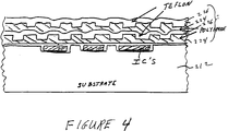
- the sublayers 24 are preferably a polyimide material and in accordance with one embodiment of the invention, may be Kapton polyimide available from E.I. DuPont de Nemours, Inc.
- the sublayers 24 are preferably each between 0.5 and 5 ⁇ m thick.
- Interleaved with the sublayers 24 are the sublayers 26 which are preferably a fluoropolymer such as Teflon available from DuPont.
- the sublayers 26 are preferably between 0.5 and 1-2 ⁇ m thick.
- AF1600 is an amorphous fluoropolymer available from DuPont Chemicals. This successful ablation of the AF1600 is a result of the thinness of the fluoropolymer layers which enable sufficient heat transfer from the underlying polyimide sublayer 24 (which does absorb the laser wavelength) to cause thermal decomposition, bond breaking or ablation in the directly overlying portion of the fluoropolymer sublayer with the result that the via hole may be drilled to the contact pad 18.
- FIG. 2 Illustrates in cross-section a two level high density interconnect structure in which both dielectric layers are in accordance with the present Invention.
- the high density interconnect structure 10′ begins with the structure 10 as illustrated in Figure 1 and has a second stacked dielectric layer 40 laminated thereover.
- the stacked dielectric layer 40 comprises a plurality of polyimide sublayers 44 and a plurality of fluoropolymer sublayers 46.
- This stacked dielectric layer is bonded to the underlying structure 10 by thermoplastic adhesive 42.
- the thermoplastic adhesive 42 in combination with the sublayers 44 and 46, form the dielectric layer 40.
- the preferred source material at this time for the fluoropolymer sublayers 46′ is the amorphous fluoropolymer AF1600 or AF2400 available from DuPont Chemicals.
- the solvent used for spinning on this material (Fluorinert FC-75 available from DuPont) may be baked out at 150°C and thus, does not present a temperature problem for a typical high density interconnect structure.
- the stacked dielectric layer 20 of Figure 1 may be formed by stacking preformed films of the polyimide material and the fluoropolymer material, applying pressure to them and heating them to above the Tg of the lower Tg material and then allowing the stack to cool. After the stack has cooled, the layers are bonded to each other to provide a single unitary structure.
- a second fluoropolymer sublayer is then spun on, dried and baked.
- the stacked dielectric layer 120 is separated from its support substrate 112. This may be done in a number of ways. One simple way is to provide a soluble layer between the substrate 112 and the first sublayer 124 of the dielectric layer 120. This soluble layer may then be dissolved out of the structure to separate the dielectric layer 120 from the substrate 112. Alternatively, the substrate 112 may be dissolved or etched to remove it from the dielectric layer 120. Other techniques may also be used. This stacked dielectric layer 120 is then ready for lamination to a high density interconnect structure in the manner which has been described. This stacked dielectric layer may also be used in other applications.
- sublayers 24 and 26 are illustrated as being substantially the same thickness, they may, instead of being substantially the same thickness, differ in thickness by a substantial amount.
- An upper limit on the fluoropolymer sublayer's thickness is just enough less than the full height of the stacked dielectric layer to enable the polyimide outer sublayers 24 to be included in the stack. In this situation, the stacked dielectric layer will not be ablatable at 351 nm for a sufficiently thick stack dielectric layer.
- that stack structure may be laser drilled at other laser wavelengths (e.g. 193 nm) where the fluoropolymer layer is substantially absorbing.
- via holes may be formed using a metal masking process and reactive ion etching (RIE). When RIE is used to form the via holes, the thickness limitations on the fluoropolymer layer which are imposed by laser ablation may be ignored. Consequently, no thickness limitations are inherent to the invention.
Landscapes
- Production Of Multi-Layered Print Wiring Board (AREA)
Applications Claiming Priority (2)
| Application Number | Priority Date | Filing Date | Title |
|---|---|---|---|
| US07/546,960 US5073814A (en) | 1990-07-02 | 1990-07-02 | Multi-sublayer dielectric layers |
| US546960 | 1990-07-02 |
Publications (2)
| Publication Number | Publication Date |
|---|---|
| EP0465197A2 true EP0465197A2 (de) | 1992-01-08 |
| EP0465197A3 EP0465197A3 (en) | 1992-04-15 |
Family
ID=24182733
Family Applications (1)
| Application Number | Title | Priority Date | Filing Date |
|---|---|---|---|
| EP19910305962 Withdrawn EP0465197A3 (en) | 1990-07-02 | 1991-07-01 | Multi-sublayer dielectric layers |
Country Status (3)
| Country | Link |
|---|---|
| US (1) | US5073814A (de) |
| EP (1) | EP0465197A3 (de) |
| JP (1) | JPH04233297A (de) |
Cited By (14)
| Publication number | Priority date | Publication date | Assignee | Title |
|---|---|---|---|---|
| EP0687004A1 (de) * | 1994-06-07 | 1995-12-13 | Texas Instruments Incorporated | Verfahren zur Herstellung von Dielektrica auf Halbleiterbauelemente |
| EP0687009A3 (de) * | 1994-06-02 | 1996-04-10 | Ibm | Mehrschichtpackung eines elektronischen Schaltkreises mit dielektrischen Polymerschichten unterschiedlichen optischen Absorptionsvermögens und Verfahren zu ihrer Herstellung |
| EP0707340A3 (de) * | 1994-10-11 | 1997-06-04 | Martin Marietta Corp | Herstellung und Strukturen von Schaltungsmodulen mit flexiblen Verdrahtungslagen |
| EP0692824A3 (de) * | 1994-07-15 | 1997-07-16 | Texas Instruments Inc | Verbesserungen in, an oder in Bezug auf Halbleiteranordnungen |
| DE19736090A1 (de) * | 1997-08-20 | 1999-03-04 | Daimler Benz Ag | Bauelement mit Schutzschicht und Verfahren zur Herstellung des Bauelements |
| US6184133B1 (en) | 1994-04-28 | 2001-02-06 | Fujitsu Limited | Method of forming an assembly board with insulator filled through holes |
| US6347037B2 (en) | 1994-04-28 | 2002-02-12 | Fujitsu Limited | Semiconductor device and method of forming the same |
| WO2002035607A3 (de) * | 2000-10-23 | 2002-10-03 | Siemens Ag | Halbleiter-anordnung und verfahren zur herstellung von derartigen halbleiter-anordnungen |
| WO2004100259A3 (de) * | 2003-05-09 | 2005-03-31 | Eupec Gmbh & Co Kg | Halbleiterbauelement und verfahren zum herstellen eines halbleiterbauelements |
| WO2007025859A3 (de) * | 2005-08-30 | 2007-04-26 | Siemens Ag | Halbleiterstruktur mit einem lateral funktionalen aufbau |
| EP1755162A3 (de) * | 2005-08-17 | 2007-10-17 | General Electric Company | Leistungshalbleitergehäusungsmethode und Struktur |
| EP1764831A3 (de) * | 2005-09-15 | 2008-03-12 | Plastic Logic Limited | Verfahren zum Herstellen von Löchern durch die Verwendung von Laserenergie |
| US7829386B2 (en) | 2005-08-17 | 2010-11-09 | General Electric Company | Power semiconductor packaging method and structure |
| EP2365523A3 (de) * | 2010-03-02 | 2013-04-03 | General Electric Company | Stressresistente Microvia-Struktur für flexible Schaltungen |
Families Citing this family (74)
| Publication number | Priority date | Publication date | Assignee | Title |
|---|---|---|---|---|
| US5410179A (en) * | 1990-04-05 | 1995-04-25 | Martin Marietta Corporation | Microwave component having tailored operating characteristics and method of tailoring |
| US5161093A (en) * | 1990-07-02 | 1992-11-03 | General Electric Company | Multiple lamination high density interconnect process and structure employing a variable crosslinking adhesive |
| US5442237A (en) * | 1991-10-21 | 1995-08-15 | Motorola Inc. | Semiconductor device having a low permittivity dielectric |
| US5759869A (en) * | 1991-12-31 | 1998-06-02 | Sgs-Thomson Microelectronics, Inc. | Method to imporve metal step coverage by contact reflow |
| US5336928A (en) * | 1992-09-18 | 1994-08-09 | General Electric Company | Hermetically sealed packaged electronic system |
| US5302547A (en) * | 1993-02-08 | 1994-04-12 | General Electric Company | Systems for patterning dielectrics by laser ablation |
| US6400573B1 (en) * | 1993-02-09 | 2002-06-04 | Texas Instruments Incorporated | Multi-chip integrated circuit module |
| US5401687A (en) * | 1993-04-15 | 1995-03-28 | Martin Marietta Corporation | Process for high density interconnection of substrates and integrated circuit chips containing sensitive structures |
| US5486493A (en) * | 1994-02-25 | 1996-01-23 | Jeng; Shin-Puu | Planarized multi-level interconnect scheme with embedded low-dielectric constant insulators |
| US5434751A (en) * | 1994-04-11 | 1995-07-18 | Martin Marietta Corporation | Reworkable high density interconnect structure incorporating a release layer |
| US6278174B1 (en) * | 1994-04-28 | 2001-08-21 | Texas Instruments Incorporated | Integrated circuit insulator and structure using low dielectric insulator material including HSQ and fluorinated oxide |
| US5561085A (en) * | 1994-12-19 | 1996-10-01 | Martin Marietta Corporation | Structure for protecting air bridges on semiconductor chips from damage |
| JP3252635B2 (ja) * | 1995-01-13 | 2002-02-04 | 株式会社村田製作所 | 積層電子部品 |
| US5552633A (en) * | 1995-06-06 | 1996-09-03 | Martin Marietta Corporation | Three-dimensional multimodule HDI arrays with heat spreading |
| US5745984A (en) * | 1995-07-10 | 1998-05-05 | Martin Marietta Corporation | Method for making an electronic module |
| US5866952A (en) * | 1995-11-30 | 1999-02-02 | Lockheed Martin Corporation | High density interconnected circuit module with a compliant layer as part of a stress-reducing molded substrate |
| US6137125A (en) * | 1995-12-21 | 2000-10-24 | The Whitaker Corporation | Two layer hermetic-like coating for on-wafer encapsulatuon of GaAs MMIC's having flip-chip bonding capabilities |
| KR100420792B1 (ko) * | 1996-09-26 | 2004-05-31 | 삼성전자주식회사 | 파워마이크로웨이브하이브리드집적회로 |
| US6054769A (en) * | 1997-01-17 | 2000-04-25 | Texas Instruments Incorporated | Low capacitance interconnect structures in integrated circuits having an adhesion and protective overlayer for low dielectric materials |
| US5818111A (en) * | 1997-03-21 | 1998-10-06 | Texas Instruments Incorporated | Low capacitance interconnect structures in integrated circuits using a stack of low dielectric materials |
| KR100214562B1 (ko) * | 1997-03-24 | 1999-08-02 | 구본준 | 적층 반도체 칩 패키지 및 그 제조 방법 |
| US6130472A (en) * | 1998-07-24 | 2000-10-10 | International Business Machines Corporation | Moisture and ion barrier for protection of devices and interconnect structures |
| FR2783354B1 (fr) * | 1998-08-25 | 2002-07-12 | Commissariat Energie Atomique | Procede collectif de conditionnement d'une pluralite de composants formes initialement dans un meme substrat |
| AU5699699A (en) * | 1998-08-31 | 2000-03-21 | Bios Group Lp | A method for optimal search on a technology landscape |
| JP2001185653A (ja) * | 1999-10-12 | 2001-07-06 | Fujitsu Ltd | 半導体装置及び基板の製造方法 |
| WO2001063991A1 (en) * | 2000-02-25 | 2001-08-30 | Ibiden Co., Ltd. | Multilayer printed wiring board and method for producing multilayer printed wiring board |
| US6627998B1 (en) * | 2000-07-27 | 2003-09-30 | International Business Machines Corporation | Wafer scale thin film package |
| KR20030060898A (ko) * | 2000-09-25 | 2003-07-16 | 이비덴 가부시키가이샤 | 반도체소자,반도체소자의 제조방법,다층프린트배선판 및다층프린트배선판의 제조방법 |
| US6774743B2 (en) | 2000-11-09 | 2004-08-10 | Merrimac Industries, Inc. | Multi-layered spiral couplers on a fluropolymer composite substrate |
| US6765455B1 (en) | 2000-11-09 | 2004-07-20 | Merrimac Industries, Inc. | Multi-layered spiral couplers on a fluropolymer composite substrate |
| US20020175402A1 (en) * | 2001-05-23 | 2002-11-28 | Mccormack Mark Thomas | Structure and method of embedding components in multi-layer substrates |
| US6720784B2 (en) * | 2001-06-20 | 2004-04-13 | Heatron, Inc. | Device for testing electronic devices |
| US6706624B1 (en) * | 2001-10-31 | 2004-03-16 | Lockheed Martin Corporation | Method for making multichip module substrates by encapsulating electrical conductors |
| US7132736B2 (en) * | 2001-10-31 | 2006-11-07 | Georgia Tech Research Corporation | Devices having compliant wafer-level packages with pillars and methods of fabrication |
| TW517361B (en) * | 2001-12-31 | 2003-01-11 | Megic Corp | Chip package structure and its manufacture process |
| TW544882B (en) | 2001-12-31 | 2003-08-01 | Megic Corp | Chip package structure and process thereof |
| US6673698B1 (en) | 2002-01-19 | 2004-01-06 | Megic Corporation | Thin film semiconductor package utilizing a glass substrate with composite polymer/metal interconnect layers |
| TW584950B (en) | 2001-12-31 | 2004-04-21 | Megic Corp | Chip packaging structure and process thereof |
| TW503496B (en) | 2001-12-31 | 2002-09-21 | Megic Corp | Chip packaging structure and manufacturing process of the same |
| TW528232U (en) * | 2002-04-12 | 2003-04-11 | Hon Hai Prec Ind Co Ltd | Small form-factor pluggable module with de-latching mechanism |
| KR100525343B1 (ko) * | 2002-08-12 | 2005-11-02 | 학교법인 한국정보통신학원 | 3차원 초고주파 다층회로를 위한 공기 공동 제작방법 |
| US6964881B2 (en) | 2002-08-27 | 2005-11-15 | Micron Technology, Inc. | Multi-chip wafer level system packages and methods of forming same |
| US6756662B2 (en) * | 2002-09-25 | 2004-06-29 | International Business Machines Corporation | Semiconductor chip module and method of manufacture of same |
| US7135780B2 (en) * | 2003-02-12 | 2006-11-14 | Micron Technology, Inc. | Semiconductor substrate for build-up packages |
| FI20031341A7 (fi) | 2003-09-18 | 2005-03-19 | Imbera Electronics Oy | Menetelmä elektroniikkamoduulin valmistamiseksi |
| FI119714B (fi) | 2005-06-16 | 2009-02-13 | Imbera Electronics Oy | Piirilevyrakenne ja menetelmä piirilevyrakenteen valmistamiseksi |
| US7367236B2 (en) * | 2005-07-21 | 2008-05-06 | The Boeing Company | Non-destructive inspection system and associated method |
| US7398698B2 (en) * | 2005-11-03 | 2008-07-15 | The Boeing Company | Smart repair patch and associated method |
| TWI285424B (en) * | 2005-12-22 | 2007-08-11 | Princo Corp | Substrate including a multi-layer interconnection structure, methods of manufacturing and recycling the same, method of packaging electronic devices by using the same, and method of manufacturing an interconnection device |
| US8051557B2 (en) * | 2006-03-31 | 2011-11-08 | Princo Corp. | Substrate with multi-layer interconnection structure and method of manufacturing the same |
| US7617730B2 (en) * | 2006-06-28 | 2009-11-17 | The Boeing Company | Ultrasonic inspection and repair mode selection |
| US7757558B2 (en) * | 2007-03-19 | 2010-07-20 | The Boeing Company | Method and apparatus for inspecting a workpiece with angularly offset ultrasonic signals |
| US7712369B2 (en) * | 2007-11-27 | 2010-05-11 | The Boeing Company | Array-based system and method for inspecting a workpiece with backscattered ultrasonic signals |
| FI20095557A0 (fi) | 2009-05-19 | 2009-05-19 | Imbera Electronics Oy | Valmistusmenetelmä ja elektroniikkamoduuli, joka tarjoaa uusia mahdollisuuksia johdevedoille |
| US20110079908A1 (en) * | 2009-10-06 | 2011-04-07 | Unisem Advanced Technologies Sdn. Bhd. | Stress buffer to protect device features |
| US8927339B2 (en) | 2010-11-22 | 2015-01-06 | Bridge Semiconductor Corporation | Method of making thermally enhanced semiconductor assembly with bump/base/flange heat spreader and build-up circuitry |
| US8595927B2 (en) * | 2011-03-17 | 2013-12-03 | Ibiden Co., Ltd. | Method for manufacturing multilayer printed wiring board |
| EP2584349A1 (de) * | 2011-10-19 | 2013-04-24 | Nxp B.V. | Verfahren zur Messung eines Moleküls, Vorrichtung und Halbleiterchip dafür |
| US9888568B2 (en) | 2012-02-08 | 2018-02-06 | Crane Electronics, Inc. | Multilayer electronics assembly and method for embedding electrical circuit components within a three dimensional module |
| US9087847B2 (en) | 2012-08-14 | 2015-07-21 | Bridge Semiconductor Corporation | Thermally enhanced interconnect substrate with embedded semiconductor device and built-in stopper and method of making the same |
| US9084382B2 (en) * | 2012-10-18 | 2015-07-14 | Infineon Technologies Austria Ag | Method of embedding an electronic component into an aperture of a substrate |
| US20150380369A1 (en) * | 2013-09-30 | 2015-12-31 | Nantong Fujitsu Microelectronics Co., Ltd | Wafer packaging structure and packaging method |
| US10037850B2 (en) * | 2014-12-18 | 2018-07-31 | 3M Innovative Properties Company | Multilayer film capacitor |
| US9230726B1 (en) | 2015-02-20 | 2016-01-05 | Crane Electronics, Inc. | Transformer-based power converters with 3D printed microchannel heat sink |
| JP2019067994A (ja) * | 2017-10-04 | 2019-04-25 | トヨタ自動車株式会社 | 積層基板とその製造方法 |
| TWI642333B (zh) | 2017-10-25 | 2018-11-21 | 欣興電子股份有限公司 | 電路板及其製造方法 |
| TWI642334B (zh) * | 2017-10-25 | 2018-11-21 | 欣興電子股份有限公司 | 電路板及其製造方法 |
| US11626448B2 (en) | 2019-03-29 | 2023-04-11 | Lumileds Llc | Fan-out light-emitting diode (LED) device substrate with embedded backplane, lighting system and method of manufacture |
| US11631594B2 (en) | 2019-11-19 | 2023-04-18 | Lumileds Llc | Fan out structure for light-emitting diode (LED) device and lighting system |
| US11777066B2 (en) | 2019-12-27 | 2023-10-03 | Lumileds Llc | Flipchip interconnected light-emitting diode package assembly |
| US11664347B2 (en) * | 2020-01-07 | 2023-05-30 | Lumileds Llc | Ceramic carrier and build up carrier for light-emitting diode (LED) array |
| US11476217B2 (en) | 2020-03-10 | 2022-10-18 | Lumileds Llc | Method of manufacturing an augmented LED array assembly |
| US11810895B2 (en) * | 2021-10-14 | 2023-11-07 | Honeywell Federal Manufacturing & Technologies, Llc | Electrical interconnect structure using metal bridges to interconnect die |
| CN118891960A (zh) * | 2022-03-29 | 2024-11-01 | 住友电气工业株式会社 | 印刷布线板用基板、印刷布线板及多层印刷布线板 |
Family Cites Families (5)
| Publication number | Priority date | Publication date | Assignee | Title |
|---|---|---|---|---|
| US3967310A (en) * | 1968-10-09 | 1976-06-29 | Hitachi, Ltd. | Semiconductor device having controlled surface charges by passivation films formed thereon |
| IL86162A (en) * | 1988-04-25 | 1991-11-21 | Zvi Orbach | Customizable semiconductor devices |
| IL78730A (en) * | 1986-05-08 | 1990-03-19 | Avner Pdahtzur | Protective optical coating and method for use thereof |
| EP0327398B1 (de) * | 1988-02-05 | 1994-09-21 | Raychem Limited | Laser-bearbeitete Polymere |
| JPH01235254A (ja) * | 1988-03-15 | 1989-09-20 | Nec Corp | 半導体装置及びその製造方法 |
-
1990
- 1990-07-02 US US07/546,960 patent/US5073814A/en not_active Expired - Fee Related
-
1991
- 1991-07-01 EP EP19910305962 patent/EP0465197A3/en not_active Withdrawn
- 1991-07-02 JP JP3186972A patent/JPH04233297A/ja not_active Withdrawn
Cited By (19)
| Publication number | Priority date | Publication date | Assignee | Title |
|---|---|---|---|---|
| US6184133B1 (en) | 1994-04-28 | 2001-02-06 | Fujitsu Limited | Method of forming an assembly board with insulator filled through holes |
| US6347037B2 (en) | 1994-04-28 | 2002-02-12 | Fujitsu Limited | Semiconductor device and method of forming the same |
| EP0685878B1 (de) * | 1994-04-28 | 2010-06-23 | Fujitsu Microelectronics Limited | Halbleiterbauelement und Verfahren zu seiner Herstellung |
| EP0687009A3 (de) * | 1994-06-02 | 1996-04-10 | Ibm | Mehrschichtpackung eines elektronischen Schaltkreises mit dielektrischen Polymerschichten unterschiedlichen optischen Absorptionsvermögens und Verfahren zu ihrer Herstellung |
| US5626771A (en) * | 1994-06-02 | 1997-05-06 | International Business Machines Corporation | Design of high density structures with laser etch stop |
| EP0687004A1 (de) * | 1994-06-07 | 1995-12-13 | Texas Instruments Incorporated | Verfahren zur Herstellung von Dielektrica auf Halbleiterbauelemente |
| EP0692824A3 (de) * | 1994-07-15 | 1997-07-16 | Texas Instruments Inc | Verbesserungen in, an oder in Bezug auf Halbleiteranordnungen |
| EP0707340A3 (de) * | 1994-10-11 | 1997-06-04 | Martin Marietta Corp | Herstellung und Strukturen von Schaltungsmodulen mit flexiblen Verdrahtungslagen |
| DE19736090B4 (de) * | 1997-08-20 | 2005-04-14 | Daimlerchrysler Ag | Bauelement mit Schutzschicht und Verfahren zur Herstellung einer Schutzschicht für ein Bauelement |
| DE19736090A1 (de) * | 1997-08-20 | 1999-03-04 | Daimler Benz Ag | Bauelement mit Schutzschicht und Verfahren zur Herstellung des Bauelements |
| WO2002035607A3 (de) * | 2000-10-23 | 2002-10-03 | Siemens Ag | Halbleiter-anordnung und verfahren zur herstellung von derartigen halbleiter-anordnungen |
| WO2004100259A3 (de) * | 2003-05-09 | 2005-03-31 | Eupec Gmbh & Co Kg | Halbleiterbauelement und verfahren zum herstellen eines halbleiterbauelements |
| EP1755162A3 (de) * | 2005-08-17 | 2007-10-17 | General Electric Company | Leistungshalbleitergehäusungsmethode und Struktur |
| US7829386B2 (en) | 2005-08-17 | 2010-11-09 | General Electric Company | Power semiconductor packaging method and structure |
| WO2007025859A3 (de) * | 2005-08-30 | 2007-04-26 | Siemens Ag | Halbleiterstruktur mit einem lateral funktionalen aufbau |
| EP1764831A3 (de) * | 2005-09-15 | 2008-03-12 | Plastic Logic Limited | Verfahren zum Herstellen von Löchern durch die Verwendung von Laserenergie |
| US8546723B2 (en) | 2005-09-15 | 2013-10-01 | Plastic Logic Limited | Forming holes using laser energy |
| EP2365523A3 (de) * | 2010-03-02 | 2013-04-03 | General Electric Company | Stressresistente Microvia-Struktur für flexible Schaltungen |
| US10276486B2 (en) | 2010-03-02 | 2019-04-30 | General Electric Company | Stress resistant micro-via structure for flexible circuits |
Also Published As
| Publication number | Publication date |
|---|---|
| EP0465197A3 (en) | 1992-04-15 |
| JPH04233297A (ja) | 1992-08-21 |
| US5073814A (en) | 1991-12-17 |
Similar Documents
| Publication | Publication Date | Title |
|---|---|---|
| US5073814A (en) | Multi-sublayer dielectric layers | |
| US5157589A (en) | Mutliple lamination high density interconnect process and structure employing thermoplastic adhesives having sequentially decreasing TG 's | |
| US5338975A (en) | High density interconnect structure including a spacer structure and a gap | |
| US5355102A (en) | HDI impedance matched microwave circuit assembly | |
| US5161093A (en) | Multiple lamination high density interconnect process and structure employing a variable crosslinking adhesive | |
| US5206712A (en) | Building block approach to microwave modules | |
| US6294741B1 (en) | Electronics module having high density interconnect structures incorporating an improved dielectric lamination adhesive | |
| US5331203A (en) | High density interconnect structure including a chamber | |
| US5559363A (en) | Off-chip impedance matching utilizing a dielectric element and high density interconnect technology | |
| US4918811A (en) | Multichip integrated circuit packaging method | |
| US4783695A (en) | Multichip integrated circuit packaging configuration and method | |
| US5434751A (en) | Reworkable high density interconnect structure incorporating a release layer | |
| US5345205A (en) | Compact high density interconnected microwave system | |
| US5527741A (en) | Fabrication and structures of circuit modules with flexible interconnect layers | |
| US5386627A (en) | Method of fabricating a multi-layer integrated circuit chip interposer | |
| US5232548A (en) | Discrete fabrication of multi-layer thin film, wiring structures | |
| US5699234A (en) | Stacking of three dimensional high density interconnect modules with metal edge contacts | |
| US6803324B2 (en) | Semiconductor device and its manufacturing method | |
| US5224265A (en) | Fabrication of discrete thin film wiring structures | |
| EP0987760B1 (de) | Herstellungsverfahren für Mehrchipmodul | |
| US5336928A (en) | Hermetically sealed packaged electronic system | |
| US5351001A (en) | Microwave component test method and apparatus | |
| US5199163A (en) | Metal transfer layers for parallel processing | |
| JPH06350020A (ja) | マルチチップ集積回路モジュール及びその製造方法 | |
| JPH08236628A (ja) | 半導体チップ上のエアブリッジを損傷から保護するための構造 |
Legal Events
| Date | Code | Title | Description |
|---|---|---|---|
| PUAI | Public reference made under article 153(3) epc to a published international application that has entered the european phase |
Free format text: ORIGINAL CODE: 0009012 |
|
| AK | Designated contracting states |
Kind code of ref document: A2 Designated state(s): DE FR GB IT |
|
| PUAL | Search report despatched |
Free format text: ORIGINAL CODE: 0009013 |
|
| AK | Designated contracting states |
Kind code of ref document: A3 Designated state(s): DE FR GB IT |
|
| 17P | Request for examination filed |
Effective date: 19920930 |
|
| 17Q | First examination report despatched |
Effective date: 19941012 |
|
| STAA | Information on the status of an ep patent application or granted ep patent |
Free format text: STATUS: THE APPLICATION IS DEEMED TO BE WITHDRAWN |
|
| 18D | Application deemed to be withdrawn |
Effective date: 19960119 |