EP1483797B1 - Becherförmiges gehäuse und kondensator mit dem gehäuse - Google Patents
Becherförmiges gehäuse und kondensator mit dem gehäuse Download PDFInfo
- Publication number
- EP1483797B1 EP1483797B1 EP03709660A EP03709660A EP1483797B1 EP 1483797 B1 EP1483797 B1 EP 1483797B1 EP 03709660 A EP03709660 A EP 03709660A EP 03709660 A EP03709660 A EP 03709660A EP 1483797 B1 EP1483797 B1 EP 1483797B1
- Authority
- EP
- European Patent Office
- Prior art keywords
- housing
- electrode
- lid
- indentations
- layer stack
- Prior art date
- Legal status (The legal status is an assumption and is not a legal conclusion. Google has not performed a legal analysis and makes no representation as to the accuracy of the status listed.)
- Expired - Lifetime
Links
- 238000007373 indentation Methods 0.000 claims abstract description 57
- 239000003990 capacitor Substances 0.000 claims description 23
- 238000010292 electrical insulation Methods 0.000 claims description 6
- 238000004804 winding Methods 0.000 claims description 6
- XAGFODPZIPBFFR-UHFFFAOYSA-N aluminium Chemical compound [Al] XAGFODPZIPBFFR-UHFFFAOYSA-N 0.000 claims description 4
- 229910052782 aluminium Inorganic materials 0.000 claims description 4
- 239000000463 material Substances 0.000 claims description 4
- 238000007789 sealing Methods 0.000 claims description 4
- 229910000838 Al alloy Inorganic materials 0.000 claims description 2
- 229920001971 elastomer Polymers 0.000 claims description 2
- 239000005060 rubber Substances 0.000 claims description 2
- 239000004411 aluminium Substances 0.000 claims 1
- 239000008151 electrolyte solution Substances 0.000 description 5
- 238000003466 welding Methods 0.000 description 4
- 238000001125 extrusion Methods 0.000 description 2
- 229920000459 Nitrile rubber Polymers 0.000 description 1
- 229910045601 alloy Inorganic materials 0.000 description 1
- 239000000956 alloy Substances 0.000 description 1
- 230000002238 attenuated effect Effects 0.000 description 1
- 239000011324 bead Substances 0.000 description 1
- 239000004020 conductor Substances 0.000 description 1
- 238000002788 crimping Methods 0.000 description 1
- 230000001419 dependent effect Effects 0.000 description 1
- 238000009434 installation Methods 0.000 description 1
- 238000009413 insulation Methods 0.000 description 1
- 238000004519 manufacturing process Methods 0.000 description 1
- 239000004033 plastic Substances 0.000 description 1
Images


Classifications
-
- H—ELECTRICITY
- H01—ELECTRIC ELEMENTS
- H01G—CAPACITORS; CAPACITORS, RECTIFIERS, DETECTORS, SWITCHING DEVICES OR LIGHT-SENSITIVE DEVICES, OF THE ELECTROLYTIC TYPE
- H01G4/00—Fixed capacitors; Processes of their manufacture
- H01G4/002—Details
- H01G4/224—Housing; Encapsulation
-
- H—ELECTRICITY
- H01—ELECTRIC ELEMENTS
- H01G—CAPACITORS; CAPACITORS, RECTIFIERS, DETECTORS, SWITCHING DEVICES OR LIGHT-SENSITIVE DEVICES, OF THE ELECTROLYTIC TYPE
- H01G9/00—Electrolytic capacitors, rectifiers, detectors, switching devices, light-sensitive or temperature-sensitive devices; Processes of their manufacture
- H01G9/004—Details
- H01G9/08—Housing; Encapsulation
-
- H—ELECTRICITY
- H01—ELECTRIC ELEMENTS
- H01M—PROCESSES OR MEANS, e.g. BATTERIES, FOR THE DIRECT CONVERSION OF CHEMICAL ENERGY INTO ELECTRICAL ENERGY
- H01M50/00—Constructional details or processes of manufacture of the non-active parts of electrochemical cells other than fuel cells, e.g. hybrid cells
- H01M50/10—Primary casings, jackets or wrappings of a single cell or a single battery
- H01M50/147—Lids or covers
- H01M50/148—Lids or covers characterised by their shape
- H01M50/152—Lids or covers characterised by their shape for cells having curved cross-section, e.g. round or elliptic
-
- H—ELECTRICITY
- H01—ELECTRIC ELEMENTS
- H01M—PROCESSES OR MEANS, e.g. BATTERIES, FOR THE DIRECT CONVERSION OF CHEMICAL ENERGY INTO ELECTRICAL ENERGY
- H01M50/00—Constructional details or processes of manufacture of the non-active parts of electrochemical cells other than fuel cells, e.g. hybrid cells
- H01M50/50—Current conducting connections for cells or batteries
- H01M50/543—Terminals
- H01M50/552—Terminals characterised by their shape
- H01M50/559—Terminals adapted for cells having curved cross-section, e.g. round, elliptic or button cells
- H01M50/56—Cup shaped terminals
-
- H—ELECTRICITY
- H01—ELECTRIC ELEMENTS
- H01M—PROCESSES OR MEANS, e.g. BATTERIES, FOR THE DIRECT CONVERSION OF CHEMICAL ENERGY INTO ELECTRICAL ENERGY
- H01M50/00—Constructional details or processes of manufacture of the non-active parts of electrochemical cells other than fuel cells, e.g. hybrid cells
- H01M50/10—Primary casings, jackets or wrappings of a single cell or a single battery
- H01M50/102—Primary casings, jackets or wrappings of a single cell or a single battery characterised by their shape or physical structure
- H01M50/107—Primary casings, jackets or wrappings of a single cell or a single battery characterised by their shape or physical structure having curved cross-section, e.g. round or elliptic
-
- Y—GENERAL TAGGING OF NEW TECHNOLOGICAL DEVELOPMENTS; GENERAL TAGGING OF CROSS-SECTIONAL TECHNOLOGIES SPANNING OVER SEVERAL SECTIONS OF THE IPC; TECHNICAL SUBJECTS COVERED BY FORMER USPC CROSS-REFERENCE ART COLLECTIONS [XRACs] AND DIGESTS
- Y02—TECHNOLOGIES OR APPLICATIONS FOR MITIGATION OR ADAPTATION AGAINST CLIMATE CHANGE
- Y02E—REDUCTION OF GREENHOUSE GAS [GHG] EMISSIONS, RELATED TO ENERGY GENERATION, TRANSMISSION OR DISTRIBUTION
- Y02E60/00—Enabling technologies; Technologies with a potential or indirect contribution to GHG emissions mitigation
- Y02E60/10—Energy storage using batteries
Definitions
- Electrodes of electrochemical cells such as capacitors or batteries are often housed in cup-shaped housings. These housings are bounded on one side by a floor and closed on the other side by a lid. On the lid are usually two electrical connections, which serve to contact the electrodes located inside the cup-shaped housing.
- additional arresters made of electrically conductive material are often either attached to the electrodes or protruding portions of the electrodes are cut so that protruding arresters are formed.
- These arresters are then connected either by means of screw with the electrical connections (see, eg Figure 1A ) or by welding firmly connected to the electrical connections.
- Such a contact between the electrodes and the electrical connections is difficult to implement and therefore very time-consuming and therefore costly in production.
- the electrodes are contacted by inwardly directed indentations of rectangular cross section, which are arranged on the inner walls, for example, the lid and the housing bottom.
- the housing cup is applied with the potential of one electrode and must be electrically isolated from the lid, which is acted upon by the potential of the other electrode.
- contact these indentations projecting portions of the electrodes with usually only a small contact surface between the indentations and the electrodes is present.
- Such contact points are often also welded, for example by means of a laser.
- the laser beam in the region of the indentation is often conical, it is attached to the External edges of the indentation attenuated in rectangular indentations, so that a very low energy input of the laser results in the interior of the indentation, so that the indentation can be insufficiently welded to the electrodes (see, eg FIG. 2B ).
- the DE 751 677 C discloses a capacitor with two contacts of an electrode, one of which has a bump.
- the EP 0 685 895 A1 , the EP 1 039 564 A1 and the US 4,213,004 disclose hermetically sealed batteries with a recess in the lid for better contact of the lid with an insulating part.
- the FR 2 585 185 A1 discloses a capacitor with a recess in the lid, which ensures better contact.
- porous separators are frequently present between the two electrodes of different polarity, which are impregnated with an electrolyte solution, so that both electrodes are in contact with the electrolyte solution.
- the invention provides a cup-shaped housing for electrochemical cells with at least two electrodes, wherein the cup-shaped housing has a cover, in which an inwardly directed first indentation for contacting a first electrode is formed and in the housing bottom of the housing cup a second inwardly directed indentation for contacting a second electrode is formed.
- the advantage of a housing according to the invention is that due to the tapered cross section of the first and second indentation results in a much larger contact area between the indentation and the electrodes, as in conventional housings.
- This special form of indentation moreover achieves a maximum frictional connection between the indentation and the electrodes. Due to the tapering in the interior of the housing cross-section of the indentations, it is particularly easily possible in the case of welding the contact point, for example by means of a laser beam to allow high energy input into the recess, so that the electrodes are particularly well merged with the indentations (see eg also Fig. 3B ).
- the first and the second indentation extend in a straight line over a large part of an expansion direction of the lid and the housing bottom.
- Such a designed housing has the advantage that a particularly large contact area between the indentations and the electrodes is created by the long spatial extent of the indentations.
- first and second indentations are each formed from a separate component which is mounted on the inside of the cover or on the inside of the housing bottom. This can be done for example by means of welding or riveting.
- the material of housings according to the invention may, for example, a number of aluminum alloys, for example aluminum 99.5 or aluminum 99.9 and aluminum wrought alloys.
- the advantage of these materials is that, on the one hand, they are readily electrically conductive, so that they can be well supplied with the potential of the electrodes, and, on the other hand, they have good deformation properties, so that they are easily processed, hot or cold, for example by extrusion can be.
- casings of this material according to the invention it is possible, for example, to mold the first and second indentations by means of extrusion. In this way, the recesses can be formed particularly advantageous in one step with the housing and with the lid.
- an electrically insulating component is provided in one piece, which runs circumferentially around the edge of the lid and is arranged tightly between the cover and the wall of the housing (see Fig. 4A ).
- first regions of the electrically insulating component are arranged circumferentially around the edge of the cover, wherein they have a notch into which the edge of the housing to the housing interior is circumferentially folded around the lid.
- the electrically insulating component may be rubber, e.g. Acrylonitrile butadiene rubber.
- the invention describes a cup-shaped housing in which electrode layers are arranged (ie, an electrochemical cell which is a capacitor). Inside the housing, a stack of layers is housed, comprising the first and the second electrode, which are formed in this case as electrode layers. Under certain circumstances, a surface-shaped separator impregnated with an electrolyte solution may be located between the electrode layers.
- the end faces of the layer stack face the lid or the housing bottom (see, for example FIG. 3A ). At the end faces of the layer stack are edge regions each of either the first or the second electrode layer over and are folded at the contact points with the recesses to increase the contact surface.
- the contact points between the indentations and the electrode layers can be welded.
- the contact layers can be laser-welded. Due to the special, tapered into the interior of the housing cross-sectional shape of the indentations can be transmitted to the weld by means of a laser beam, a particularly high energy input, so that can be particularly well welded by means of a laser beam.
- the layer stack described here can also be rolled up to a capacitor winding.
- FIGS. 2A and 2B show a conventional condenser with indentations having a rectangular cross section, in cross section and in detail.
- FIGS. 3A and 3B show a capacitor with a housing according to the invention in cross-section and in detail.
- FIGS. 4A and 4B show a capacitor with a further variant of a housing according to the invention in cross section and in plan view.
- FIG. 1A is a capacitor with a conventional housing to see.
- the capacitor housing 1 is a layer stack, which consists of a first electrode layer 16 of a second electrode layer 17 and a separator 14 located therebetween.
- the separator is usually impregnated with an electrolyte solution.
- On the cover 5 of the housing 1 are electrical connections 25, the first and second electrode layer via arrester 50th contact, which are attached to the electrode layers. Such contacting of the electrical connections with the electrode layers is, as described above, to be realized only with great difficulty.
- Layer stack shown can also be a capacitor winding introduced into the housing.
- a first electrode layer 16, a separator 14, and a second electrode layer 17 are wound around a core tube or a mandrel, after the removal of which the hole 20 remains.
- the respective electrode layers can be contacted via projecting arresters 50.
- FIG. 2A shows a further embodiment of a conventional housing capacitor. It can be seen that in the housing 1, the capacitor winding 15 is introduced, wherein in the middle of the capacitor winding 15, the hole 20 which remains after the removal of the core tube or the mandrel.
- the lid 5 with the electrical connection 25 has an inwardly directed cross-sectionally rectangular indentation 5a, which contacts the protruding areas 16a of the second electrode layer 16. The capacitor cover is therefore exposed to the potential of the first electrode layer.
- a second indentation 10a which is also rectangular in cross-section and this contacts the protruding portions 17a of the second electrode layer 17.
- the housing cup is thus subjected to the potential of the second electrode layer.
- an electrical insulation 6 is located between the housing cup and the lid, an electrical insulation 6.
- FIG. 2B is to be seen enlarged in Figure 2a denoted by 11 circle.
- the second recess 10a in this case has only a very small contact surface 17C to the protruding portions 17A of the second electrode layer 17 due to the rectangular cross section.
- the cone 30 of a laser beam is shown. It can be clearly seen that the outer edges 10B of the indentation 10A protrude into the laser cone 30 and thus reduce the energy input of the laser into the indentation. Due to this reduction of the energy input, during welding, there is no such good connection between the indentation 10A and the contact surface 17C with the protruding regions 17A of the second electrode layer.
- FIG. 3a is to see a capacitor with a housing according to the invention.
- Both in the lid 5 and in the bottom of the cup are inwardly directed indentations 5B and 10B. Both indentations have a tapering cross-section on the inside.
- FIG. 3B is the in FIG. 3A shown magnified with 12 circles. It can be seen that due to the tapering cross-section of the recess 10B, particularly large contact surfaces 17D between the recess and the overhanging regions 17A of the second electrode layer 17 result. In this case, the overhanging areas of the electrode layers may be folded over at the contact point so that possibly two or more electrode layers are superimposed and compressed, so that a particularly good contact between the indentation and the electrode layers results.
- a conical laser beam 30 which is shown here schematically, is not weakened by the edges of the indentation, so that a particularly good energy input of the laser beam is possible and thus a particularly good weld between the indentation and the contact points 17D the overhanging areas of the electrode layer is possible.
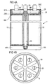
- FIG. 4A shows a capacitor with a further variant of a housing according to the invention.
- the indentations are formed elongated both in the lid and in the cup bottom.
- This special shape of the indentations results in a particularly large Contact surface between the indentations and the electrode layers.
- an electrically insulating component 21 is present. This component 21 is arranged tightly between the cover 5 and the wall of the housing 1 and thus at the same time electrically insulates the cover from the housing and seals the housing.
- First regions 21A of the electrically insulating component are arranged outside the housing, surrounding the cover, and have a notch 21C into which the edge of the housing is folded.
- the electrically insulating member 21 can be realized inside the housing.
- second regions 21B of the electrically insulating component which are arranged between the wall of the housing and the protruding edge regions 16A of the first electrode layer. These areas 21B particularly easily insulate the projecting edge areas of the electrode from the housing.
- a circumferential indentation 26 in the form of a bead is formed, which additionally fixes the electrically insulating component 21.
- FIG. 4B is the lid of the in FIG. 4A to see the housing shown in the supervision. It can be seen that six star-shaped indentations 5B are present in the housing cover, which can produce a particularly intimate contact with the electrode layer. Furthermore, one or more electrical connections 25 are formed on the housing.
- the invention is not limited to the embodiments shown here. Other variations are possible both in terms of the number of indentations in the housing, as well as with respect to their shapes.
- the electrodes, which are contacted by means of the indentations, can likewise have different shapes. Thus, for example, in addition to the layer stack shown also wound, or differently shaped electrodes into consideration.
Applications Claiming Priority (3)
| Application Number | Priority Date | Filing Date | Title |
|---|---|---|---|
| DE20204027U | 2002-03-13 | ||
| DE20204027U DE20204027U1 (de) | 2002-03-13 | 2002-03-13 | Becherförmiges Gehäuse und Kondensator mit dem Gehäuse |
| PCT/DE2003/000688 WO2003079464A2 (de) | 2002-03-13 | 2003-03-04 | Becherförmiges gehäuse und kondensator mit dem gehäuse |
Publications (2)
| Publication Number | Publication Date |
|---|---|
| EP1483797A2 EP1483797A2 (de) | 2004-12-08 |
| EP1483797B1 true EP1483797B1 (de) | 2009-11-11 |
Family
ID=7968910
Family Applications (1)
| Application Number | Title | Priority Date | Filing Date |
|---|---|---|---|
| EP03709660A Expired - Lifetime EP1483797B1 (de) | 2002-03-13 | 2003-03-04 | Becherförmiges gehäuse und kondensator mit dem gehäuse |
Country Status (6)
| Country | Link |
|---|---|
| US (1) | US7016178B2 (ja) |
| EP (1) | EP1483797B1 (ja) |
| JP (1) | JP2005520344A (ja) |
| AT (1) | ATE448576T1 (ja) |
| DE (2) | DE20204027U1 (ja) |
| WO (1) | WO2003079464A2 (ja) |
Families Citing this family (31)
| Publication number | Priority date | Publication date | Assignee | Title |
|---|---|---|---|---|
| DE10302119A1 (de) * | 2003-01-21 | 2004-07-29 | Epcos Ag | Elektrode für eine elektrochemische Zelle, Elektrodenwickel und elektrochemische Zelle |
| US7791860B2 (en) | 2003-07-09 | 2010-09-07 | Maxwell Technologies, Inc. | Particle based electrodes and methods of making same |
| US7352558B2 (en) | 2003-07-09 | 2008-04-01 | Maxwell Technologies, Inc. | Dry particle based capacitor and methods of making same |
| US7920371B2 (en) | 2003-09-12 | 2011-04-05 | Maxwell Technologies, Inc. | Electrical energy storage devices with separator between electrodes and methods for fabricating the devices |
| EP1691384B1 (en) * | 2003-12-03 | 2013-02-27 | Panasonic Corporation | Coin-shaped storage cell |
| US7090946B2 (en) | 2004-02-19 | 2006-08-15 | Maxwell Technologies, Inc. | Composite electrode and method for fabricating same |
| JP2005303062A (ja) | 2004-04-13 | 2005-10-27 | Rubycon Corp | 電解コンデンサ駆動用電解液及び電解コンデンサ |
| DE112005001007T5 (de) * | 2004-05-28 | 2007-06-28 | Matsushita Electric Industrial Co., Ltd., Kadoma | Kondensator und Verfahren zu dessen Herstellung |
| FR2871615B1 (fr) * | 2004-06-11 | 2006-09-08 | Batscap Sa | Couvercle de supercondensateur avec borne centrale integree |
| KR100897638B1 (ko) * | 2004-11-25 | 2009-05-14 | 파나소닉 주식회사 | 코인형 전기화학 소자의 제조방법 및 코인형 전기화학 소자 |
| DE102004059446A1 (de) * | 2004-12-09 | 2006-06-22 | Epcos Ag | Gehäuse für elektrochemische Zellen, Stempelvorrichtung und Verfahren zur Herstellung des Gehäuses |
| US7492574B2 (en) * | 2005-03-14 | 2009-02-17 | Maxwell Technologies, Inc. | Coupling of cell to housing |
| US7440258B2 (en) | 2005-03-14 | 2008-10-21 | Maxwell Technologies, Inc. | Thermal interconnects for coupling energy storage devices |
| DE102005053397A1 (de) * | 2005-11-09 | 2007-05-10 | Semikron Elektronik Gmbh & Co. Kg | Drehstromumrichter und Kondensatoreinheit für einen Drehstromumrichter |
| JP4952123B2 (ja) * | 2005-12-13 | 2012-06-13 | パナソニック株式会社 | コンデンサユニット |
| DE102006005832B4 (de) * | 2006-02-08 | 2008-11-06 | Epcos Ag | Kondensator mit einem Kondensatorwickel und Verfahren zur Herstellung |
| WO2007122894A1 (ja) * | 2006-03-23 | 2007-11-01 | Matsushita Electric Industrial Co., Ltd. | 電気二重層コンデンサとその製造方法 |
| JP2007265846A (ja) * | 2006-03-29 | 2007-10-11 | Sanyo Electric Co Ltd | 円筒形電池およびその製造方法 |
| JP5040698B2 (ja) * | 2007-02-14 | 2012-10-03 | パナソニック株式会社 | キャパシタ |
| JP5130942B2 (ja) * | 2008-02-14 | 2013-01-30 | パナソニック株式会社 | キャパシタ |
| JP5210137B2 (ja) * | 2008-12-10 | 2013-06-12 | 株式会社神戸製鋼所 | 二次電池用円形容器 |
| KR101049282B1 (ko) * | 2009-03-03 | 2011-07-13 | 주식회사 네스캡 | 전기에너지 저장장치 |
| KR101228700B1 (ko) * | 2009-05-14 | 2013-02-01 | 파나소닉 주식회사 | 커패시터 |
| DE102015207070A1 (de) * | 2015-04-17 | 2016-10-20 | Varta Microbattery Gmbh | Batterie mit prismatischem Metallgehäuse |
| DE102016105696A1 (de) * | 2016-03-29 | 2017-10-19 | Epcos Ag | Elektrolytkondensator |
| US11830672B2 (en) | 2016-11-23 | 2023-11-28 | KYOCERA AVX Components Corporation | Ultracapacitor for use in a solder reflow process |
| JPWO2022091862A1 (ja) * | 2020-10-30 | 2022-05-05 | ||
| DE102021206490A1 (de) * | 2021-06-23 | 2022-12-29 | Trumpf Laser- Und Systemtechnik Gmbh | Verfahren und Vorrichtung zum Erzeugen einer Schweißkontur mit mehreren Laserspots über eine Scanneroptik |
| DE102021206488A1 (de) * | 2021-06-23 | 2022-12-29 | Trumpf Laser- Und Systemtechnik Gmbh | Verfahren zum mehrfachen Abfahren einer Schweißkontur mit mehreren Laserspots |
| DE102021206486A1 (de) * | 2021-06-23 | 2022-12-29 | Trumpf Laser- Und Systemtechnik Gmbh | Verfahren zum mediendichten Verschweißen von aluminiumhaltigen Bauteilen |
| DE102022111706A1 (de) | 2022-05-10 | 2023-11-16 | Monbat New Power GmbH | Verfahren zur Herstellung eines Akkumulators und Akkumulator |
Family Cites Families (19)
| Publication number | Priority date | Publication date | Assignee | Title |
|---|---|---|---|---|
| DE751677C (de) | 1942-02-24 | 1953-08-17 | Siemens & Halske A G | Verfahren zur dichten Befestigung von selbstaendig hergestellten isolierten Stromdurchfuehrungen |
| US3463969A (en) * | 1967-07-25 | 1969-08-26 | Aerovox Corp | Pressure vented electrolytic capacitor |
| NL7712605A (nl) * | 1977-11-16 | 1979-05-18 | Philips Nv | Explosieveilige elektrolytische kondensator. |
| US4213004A (en) * | 1978-06-30 | 1980-07-15 | The United States Of America As Represented By The Secretary Of The Air Force | Hermetic electrical feedthrough for aluminum housing and method of making same |
| JPS57204655U (ja) * | 1981-06-24 | 1982-12-27 | ||
| DE3325343A1 (de) * | 1983-07-13 | 1985-01-24 | Siemens AG, 1000 Berlin und 8000 München | Elektrischer kondensator mit ueberdruckabreisssicherung |
| FR2585185B1 (fr) * | 1985-07-16 | 1987-09-25 | Accumulateurs Fixes | Capot metallique pour piles electriques et piles electriques en faisant application |
| JPH0436099Y2 (ja) * | 1986-08-11 | 1992-08-26 | ||
| JP2897104B2 (ja) | 1994-06-03 | 1999-05-31 | 古河電池株式会社 | 密閉型アルカリ蓄電池の製造方法 |
| JPH11251190A (ja) * | 1997-12-22 | 1999-09-17 | Asahi Glass Co Ltd | 電気二重層キャパシタ |
| JP2000188236A (ja) * | 1998-12-21 | 2000-07-04 | Asahi Glass Co Ltd | 電気二重層キャパシタ |
| JP2000260664A (ja) * | 1999-03-11 | 2000-09-22 | Matsushita Electric Ind Co Ltd | コンデンサ |
| JP4278222B2 (ja) | 1999-03-17 | 2009-06-10 | 三洋電機株式会社 | 密閉式電池用封口板、密閉式電池及びその製造方法 |
| JP2000340210A (ja) * | 1999-05-25 | 2000-12-08 | Sanyo Electric Co Ltd | 電気エネルギー蓄積デバイス |
| JP3252846B2 (ja) * | 1999-06-01 | 2002-02-04 | 日本電気株式会社 | 非水電解液二次電池およびその製造方法 |
| JP2001068379A (ja) * | 1999-08-24 | 2001-03-16 | Honda Motor Co Ltd | 電気二重層コンデンサ |
| JP2001135358A (ja) * | 1999-08-24 | 2001-05-18 | Toyota Central Res & Dev Lab Inc | 密閉二次電池 |
| JP2002083739A (ja) * | 2000-09-07 | 2002-03-22 | Honda Motor Co Ltd | 電気二重層キャパシタ |
| FI113210B (fi) * | 2001-05-11 | 2004-03-15 | Abb Oy | Menetelmä elektrolyyttikondensaattorin jäähdyttämiseksi ja elektrolyyttikondensaattori |
-
2002
- 2002-03-13 DE DE20204027U patent/DE20204027U1/de not_active Expired - Lifetime
-
2003
- 2003-03-04 EP EP03709660A patent/EP1483797B1/de not_active Expired - Lifetime
- 2003-03-04 DE DE50312106T patent/DE50312106D1/de not_active Expired - Lifetime
- 2003-03-04 WO PCT/DE2003/000688 patent/WO2003079464A2/de active Application Filing
- 2003-03-04 US US10/507,386 patent/US7016178B2/en not_active Expired - Lifetime
- 2003-03-04 AT AT03709660T patent/ATE448576T1/de not_active IP Right Cessation
- 2003-03-04 JP JP2003577356A patent/JP2005520344A/ja active Pending
Also Published As
| Publication number | Publication date |
|---|---|
| JP2005520344A (ja) | 2005-07-07 |
| EP1483797A2 (de) | 2004-12-08 |
| ATE448576T1 (de) | 2009-11-15 |
| US7016178B2 (en) | 2006-03-21 |
| WO2003079464A2 (de) | 2003-09-25 |
| WO2003079464A3 (de) | 2003-12-04 |
| DE20204027U1 (de) | 2002-06-06 |
| DE50312106D1 (de) | 2009-12-24 |
| US20050225926A1 (en) | 2005-10-13 |
Similar Documents
| Publication | Publication Date | Title |
|---|---|---|
| EP1483797B1 (de) | Becherförmiges gehäuse und kondensator mit dem gehäuse | |
| DE102012217451A1 (de) | Batteriezelle mit in Gehäusedeckplatte integriertem Knackfederbereich | |
| DE102015121294A1 (de) | Herstellungsverfahren für eine Sekundärbatterie und eine Sekundärbatterie | |
| DE102017200823A1 (de) | Energiespeichervorrichtung, Energiespeichergerät und Verfahren zum Herstellen der Energiespeichervorrichtung | |
| DE112005001007T5 (de) | Kondensator und Verfahren zu dessen Herstellung | |
| DE112013004439T5 (de) | Elektrische Speichervorrichtung | |
| DE10332093B4 (de) | Verfahren zur Herstellung einer elektrochemischen Zelle sowie die elektrochemische Zelle | |
| DE102021006016A1 (de) | Rundzelle für einen elektrischen Energiespeicher eines Kraftfahrzeugs, insbesondere eines Kraftwagens | |
| DE112019002090T5 (de) | Abdeckplattenanordnung für eine Lithium-Ionen-Batterie und Energiespeichervorrichtung | |
| DE19524870C2 (de) | Schutzvorrichtung zum Schutz vor Überladung und zu hohen Ladeströmen beim Aufladen von Batteriezellen und Batteriezelle mit einer derartigen Schutzvorrichtung | |
| WO2020156951A1 (de) | Energiespeicherzelle, batteriemodul und herstellungsverfahren | |
| EP3745490B1 (de) | Verfahren zur herstellung einer batterie und gemäss dem verfahren hergestellte batterie | |
| WO2014040791A1 (de) | Batteriezelle mit in gehäusedeckplatte integrierter berstscheibe | |
| DE112018005366T5 (de) | Energiespeichereinrichtung | |
| EP3284119B1 (de) | Batterie mit prismatischem metallgehäuse | |
| EP1500159B1 (de) | Schmelzkarbonatbrennstoffzelle und verfahren zur herstellung einer solchen | |
| DE3332174A1 (de) | Elektrochemische zelle sowie herstellungsverfahren hierfuer | |
| DE102022103726B3 (de) | Batteriezelle | |
| DE102022107471B3 (de) | Batteriezelle und Verfahren zu ihrer Herstellung | |
| DE102013206636A1 (de) | Batteriezelle mit einem aus mindestens zwei Teilen bestehenden Deckel sowie ein Verfahren zur Herstellung einer Batteriezelle | |
| DE102021209474A1 (de) | Batteriezelle für ein Hochvoltbatteriesystem | |
| DE102022000036A1 (de) | Deckelbaugruppe für eine Batterieeinzelzelle | |
| DE102022103728B3 (de) | Batteriezelle | |
| WO2023138843A1 (de) | Elektrische durchführung und energiespeicher mit einer solchen durchführung | |
| WO2024046908A1 (de) | Batteriezelle, system, verfahren zur herstellung eines batteriezellverbunds und batteriezellverbund |
Legal Events
| Date | Code | Title | Description |
|---|---|---|---|
| PUAI | Public reference made under article 153(3) epc to a published international application that has entered the european phase |
Free format text: ORIGINAL CODE: 0009012 |
|
| 17P | Request for examination filed |
Effective date: 20040809 |
|
| AK | Designated contracting states |
Kind code of ref document: A2 Designated state(s): AT BE BG CH CY CZ DE DK EE ES FI FR GB GR HU IE IT LI LU MC NL PT RO SE SI SK TR |
|
| 17Q | First examination report despatched |
Effective date: 20090324 |
|
| GRAP | Despatch of communication of intention to grant a patent |
Free format text: ORIGINAL CODE: EPIDOSNIGR1 |
|
| GRAS | Grant fee paid |
Free format text: ORIGINAL CODE: EPIDOSNIGR3 |
|
| GRAA | (expected) grant |
Free format text: ORIGINAL CODE: 0009210 |
|
| AK | Designated contracting states |
Kind code of ref document: B1 Designated state(s): AT BE BG CH CY CZ DE DK EE ES FI FR GB GR HU IE IT LI LU MC NL PT RO SE SI SK TR |
|
| REG | Reference to a national code |
Ref country code: GB Ref legal event code: FG4D Free format text: NOT ENGLISH |
|
| REG | Reference to a national code |
Ref country code: CH Ref legal event code: EP |
|
| REG | Reference to a national code |
Ref country code: IE Ref legal event code: FG4D |
|
| REF | Corresponds to: |
Ref document number: 50312106 Country of ref document: DE Date of ref document: 20091224 Kind code of ref document: P |
|
| NLV1 | Nl: lapsed or annulled due to failure to fulfill the requirements of art. 29p and 29m of the patents act | ||
| PG25 | Lapsed in a contracting state [announced via postgrant information from national office to epo] |
Ref country code: SE Free format text: LAPSE BECAUSE OF FAILURE TO SUBMIT A TRANSLATION OF THE DESCRIPTION OR TO PAY THE FEE WITHIN THE PRESCRIBED TIME-LIMIT Effective date: 20091111 Ref country code: FI Free format text: LAPSE BECAUSE OF FAILURE TO SUBMIT A TRANSLATION OF THE DESCRIPTION OR TO PAY THE FEE WITHIN THE PRESCRIBED TIME-LIMIT Effective date: 20091111 Ref country code: ES Free format text: LAPSE BECAUSE OF FAILURE TO SUBMIT A TRANSLATION OF THE DESCRIPTION OR TO PAY THE FEE WITHIN THE PRESCRIBED TIME-LIMIT Effective date: 20100222 Ref country code: PT Free format text: LAPSE BECAUSE OF FAILURE TO SUBMIT A TRANSLATION OF THE DESCRIPTION OR TO PAY THE FEE WITHIN THE PRESCRIBED TIME-LIMIT Effective date: 20100311 |
|
| PG25 | Lapsed in a contracting state [announced via postgrant information from national office to epo] |
Ref country code: SI Free format text: LAPSE BECAUSE OF FAILURE TO SUBMIT A TRANSLATION OF THE DESCRIPTION OR TO PAY THE FEE WITHIN THE PRESCRIBED TIME-LIMIT Effective date: 20091111 Ref country code: CY Free format text: LAPSE BECAUSE OF FAILURE TO SUBMIT A TRANSLATION OF THE DESCRIPTION OR TO PAY THE FEE WITHIN THE PRESCRIBED TIME-LIMIT Effective date: 20091111 |
|
| REG | Reference to a national code |
Ref country code: IE Ref legal event code: FD4D |
|
| PG25 | Lapsed in a contracting state [announced via postgrant information from national office to epo] |
Ref country code: BG Free format text: LAPSE BECAUSE OF FAILURE TO SUBMIT A TRANSLATION OF THE DESCRIPTION OR TO PAY THE FEE WITHIN THE PRESCRIBED TIME-LIMIT Effective date: 20100211 Ref country code: EE Free format text: LAPSE BECAUSE OF FAILURE TO SUBMIT A TRANSLATION OF THE DESCRIPTION OR TO PAY THE FEE WITHIN THE PRESCRIBED TIME-LIMIT Effective date: 20091111 Ref country code: DK Free format text: LAPSE BECAUSE OF FAILURE TO SUBMIT A TRANSLATION OF THE DESCRIPTION OR TO PAY THE FEE WITHIN THE PRESCRIBED TIME-LIMIT Effective date: 20091111 Ref country code: RO Free format text: LAPSE BECAUSE OF FAILURE TO SUBMIT A TRANSLATION OF THE DESCRIPTION OR TO PAY THE FEE WITHIN THE PRESCRIBED TIME-LIMIT Effective date: 20091111 Ref country code: IE Free format text: LAPSE BECAUSE OF FAILURE TO SUBMIT A TRANSLATION OF THE DESCRIPTION OR TO PAY THE FEE WITHIN THE PRESCRIBED TIME-LIMIT Effective date: 20091111 |
|
| PG25 | Lapsed in a contracting state [announced via postgrant information from national office to epo] |
Ref country code: CZ Free format text: LAPSE BECAUSE OF FAILURE TO SUBMIT A TRANSLATION OF THE DESCRIPTION OR TO PAY THE FEE WITHIN THE PRESCRIBED TIME-LIMIT Effective date: 20091111 Ref country code: SK Free format text: LAPSE BECAUSE OF FAILURE TO SUBMIT A TRANSLATION OF THE DESCRIPTION OR TO PAY THE FEE WITHIN THE PRESCRIBED TIME-LIMIT Effective date: 20091111 |
|
| PLBE | No opposition filed within time limit |
Free format text: ORIGINAL CODE: 0009261 |
|
| STAA | Information on the status of an ep patent application or granted ep patent |
Free format text: STATUS: NO OPPOSITION FILED WITHIN TIME LIMIT |
|
| BERE | Be: lapsed |
Owner name: EPCOS A.G. Effective date: 20100331 |
|
| 26N | No opposition filed |
Effective date: 20100812 |
|
| PG25 | Lapsed in a contracting state [announced via postgrant information from national office to epo] |
Ref country code: GR Free format text: LAPSE BECAUSE OF FAILURE TO SUBMIT A TRANSLATION OF THE DESCRIPTION OR TO PAY THE FEE WITHIN THE PRESCRIBED TIME-LIMIT Effective date: 20100212 Ref country code: MC Free format text: LAPSE BECAUSE OF NON-PAYMENT OF DUE FEES Effective date: 20100331 |
|
| REG | Reference to a national code |
Ref country code: CH Ref legal event code: PL |
|
| PG25 | Lapsed in a contracting state [announced via postgrant information from national office to epo] |
Ref country code: BE Free format text: LAPSE BECAUSE OF NON-PAYMENT OF DUE FEES Effective date: 20100331 Ref country code: CH Free format text: LAPSE BECAUSE OF NON-PAYMENT OF DUE FEES Effective date: 20100331 Ref country code: LI Free format text: LAPSE BECAUSE OF NON-PAYMENT OF DUE FEES Effective date: 20100331 |
|
| PG25 | Lapsed in a contracting state [announced via postgrant information from national office to epo] |
Ref country code: IT Free format text: LAPSE BECAUSE OF FAILURE TO SUBMIT A TRANSLATION OF THE DESCRIPTION OR TO PAY THE FEE WITHIN THE PRESCRIBED TIME-LIMIT Effective date: 20091111 |
|
| PG25 | Lapsed in a contracting state [announced via postgrant information from national office to epo] |
Ref country code: AT Free format text: LAPSE BECAUSE OF NON-PAYMENT OF DUE FEES Effective date: 20100304 |
|
| PG25 | Lapsed in a contracting state [announced via postgrant information from national office to epo] |
Ref country code: HU Free format text: LAPSE BECAUSE OF FAILURE TO SUBMIT A TRANSLATION OF THE DESCRIPTION OR TO PAY THE FEE WITHIN THE PRESCRIBED TIME-LIMIT Effective date: 20100512 Ref country code: NL Free format text: LAPSE BECAUSE OF FAILURE TO SUBMIT A TRANSLATION OF THE DESCRIPTION OR TO PAY THE FEE WITHIN THE PRESCRIBED TIME-LIMIT Effective date: 20091111 Ref country code: LU Free format text: LAPSE BECAUSE OF NON-PAYMENT OF DUE FEES Effective date: 20100304 |
|
| PG25 | Lapsed in a contracting state [announced via postgrant information from national office to epo] |
Ref country code: TR Free format text: LAPSE BECAUSE OF FAILURE TO SUBMIT A TRANSLATION OF THE DESCRIPTION OR TO PAY THE FEE WITHIN THE PRESCRIBED TIME-LIMIT Effective date: 20091111 |
|
| PGFP | Annual fee paid to national office [announced via postgrant information from national office to epo] |
Ref country code: FR Payment date: 20140319 Year of fee payment: 12 |
|
| PGFP | Annual fee paid to national office [announced via postgrant information from national office to epo] |
Ref country code: GB Payment date: 20140324 Year of fee payment: 12 |
|
| GBPC | Gb: european patent ceased through non-payment of renewal fee |
Effective date: 20150304 |
|
| REG | Reference to a national code |
Ref country code: FR Ref legal event code: ST Effective date: 20151130 |
|
| PG25 | Lapsed in a contracting state [announced via postgrant information from national office to epo] |
Ref country code: GB Free format text: LAPSE BECAUSE OF NON-PAYMENT OF DUE FEES Effective date: 20150304 |
|
| PG25 | Lapsed in a contracting state [announced via postgrant information from national office to epo] |
Ref country code: FR Free format text: LAPSE BECAUSE OF NON-PAYMENT OF DUE FEES Effective date: 20150331 |
|
| PGFP | Annual fee paid to national office [announced via postgrant information from national office to epo] |
Ref country code: DE Payment date: 20170322 Year of fee payment: 15 |
|
| REG | Reference to a national code |
Ref country code: DE Ref legal event code: R119 Ref document number: 50312106 Country of ref document: DE |
|
| PG25 | Lapsed in a contracting state [announced via postgrant information from national office to epo] |
Ref country code: DE Free format text: LAPSE BECAUSE OF NON-PAYMENT OF DUE FEES Effective date: 20181002 |