EP1476899B1 - Verfahren zur herstellung von oxidschichten mit unterschiedlicher dicke auf einer substratoberfläche - Google Patents
Verfahren zur herstellung von oxidschichten mit unterschiedlicher dicke auf einer substratoberfläche Download PDFInfo
- Publication number
- EP1476899B1 EP1476899B1 EP02787067A EP02787067A EP1476899B1 EP 1476899 B1 EP1476899 B1 EP 1476899B1 EP 02787067 A EP02787067 A EP 02787067A EP 02787067 A EP02787067 A EP 02787067A EP 1476899 B1 EP1476899 B1 EP 1476899B1
- Authority
- EP
- European Patent Office
- Prior art keywords
- oxide
- layer
- substrate
- thickness
- predefined
- Prior art date
- Legal status (The legal status is an assumption and is not a legal conclusion. Google has not performed a legal analysis and makes no representation as to the accuracy of the status listed.)
- Expired - Lifetime
Links
- 239000000758 substrate Substances 0.000 title claims description 128
- 238000000034 method Methods 0.000 title claims description 104
- 230000000873 masking effect Effects 0.000 claims description 24
- 238000005530 etching Methods 0.000 claims description 18
- QJGQUHMNIGDVPM-UHFFFAOYSA-N nitrogen group Chemical group [N] QJGQUHMNIGDVPM-UHFFFAOYSA-N 0.000 claims description 14
- 238000001039 wet etching Methods 0.000 claims description 12
- 239000000203 mixture Substances 0.000 claims description 10
- -1 ammonium peroxide Chemical class 0.000 claims description 3
- 238000001312 dry etching Methods 0.000 claims description 3
- 230000009977 dual effect Effects 0.000 description 14
- GQPLMRYTRLFLPF-UHFFFAOYSA-N Nitrous Oxide Chemical compound [O-][N+]#N GQPLMRYTRLFLPF-UHFFFAOYSA-N 0.000 description 9
- MWUXSHHQAYIFBG-UHFFFAOYSA-N Nitric oxide Chemical compound O=[N] MWUXSHHQAYIFBG-UHFFFAOYSA-N 0.000 description 8
- 238000007254 oxidation reaction Methods 0.000 description 8
- 230000003647 oxidation Effects 0.000 description 7
- 238000000137 annealing Methods 0.000 description 6
- 230000008901 benefit Effects 0.000 description 6
- XUIMIQQOPSSXEZ-UHFFFAOYSA-N Silicon Chemical compound [Si] XUIMIQQOPSSXEZ-UHFFFAOYSA-N 0.000 description 5
- 230000015572 biosynthetic process Effects 0.000 description 5
- 238000005229 chemical vapour deposition Methods 0.000 description 5
- 238000004519 manufacturing process Methods 0.000 description 5
- 238000012545 processing Methods 0.000 description 5
- 238000000151 deposition Methods 0.000 description 4
- 238000002955 isolation Methods 0.000 description 4
- 239000001272 nitrous oxide Substances 0.000 description 4
- 229920002120 photoresistant polymer Polymers 0.000 description 4
- 229910052710 silicon Inorganic materials 0.000 description 4
- 239000010703 silicon Substances 0.000 description 4
- QGZKDVFQNNGYKY-UHFFFAOYSA-N Ammonia Chemical compound N QGZKDVFQNNGYKY-UHFFFAOYSA-N 0.000 description 3
- 150000002500 ions Chemical class 0.000 description 3
- 230000002829 reductive effect Effects 0.000 description 3
- 238000013459 approach Methods 0.000 description 2
- 230000003247 decreasing effect Effects 0.000 description 2
- 230000007547 defect Effects 0.000 description 2
- 230000008021 deposition Effects 0.000 description 2
- 238000011161 development Methods 0.000 description 2
- 238000012986 modification Methods 0.000 description 2
- 230000004048 modification Effects 0.000 description 2
- 239000004065 semiconductor Substances 0.000 description 2
- VYPSYNLAJGMNEJ-UHFFFAOYSA-N Silicium dioxide Chemical compound O=[Si]=O VYPSYNLAJGMNEJ-UHFFFAOYSA-N 0.000 description 1
- 229910021529 ammonia Inorganic materials 0.000 description 1
- 230000003466 anti-cipated effect Effects 0.000 description 1
- QVGXLLKOCUKJST-UHFFFAOYSA-N atomic oxygen Chemical compound [O] QVGXLLKOCUKJST-UHFFFAOYSA-N 0.000 description 1
- 239000002800 charge carrier Substances 0.000 description 1
- 238000010276 construction Methods 0.000 description 1
- 230000006378 damage Effects 0.000 description 1
- 238000013461 design Methods 0.000 description 1
- 238000009792 diffusion process Methods 0.000 description 1
- 239000002019 doping agent Substances 0.000 description 1
- 230000000694 effects Effects 0.000 description 1
- 238000010292 electrical insulation Methods 0.000 description 1
- 239000011810 insulating material Substances 0.000 description 1
- 230000010354 integration Effects 0.000 description 1
- 230000000670 limiting effect Effects 0.000 description 1
- 239000000463 material Substances 0.000 description 1
- 238000005259 measurement Methods 0.000 description 1
- 239000002184 metal Substances 0.000 description 1
- 229910044991 metal oxide Inorganic materials 0.000 description 1
- 150000004706 metal oxides Chemical class 0.000 description 1
- 150000004767 nitrides Chemical class 0.000 description 1
- 229910000069 nitrogen hydride Inorganic materials 0.000 description 1
- 239000001301 oxygen Substances 0.000 description 1
- 229910052760 oxygen Inorganic materials 0.000 description 1
- 230000036961 partial effect Effects 0.000 description 1
- 229910021420 polycrystalline silicon Inorganic materials 0.000 description 1
- 229920005591 polysilicon Polymers 0.000 description 1
- 230000002028 premature Effects 0.000 description 1
- 230000009528 severe injury Effects 0.000 description 1
- 229910021332 silicide Inorganic materials 0.000 description 1
- FVBUAEGBCNSCDD-UHFFFAOYSA-N silicide(4-) Chemical compound [Si-4] FVBUAEGBCNSCDD-UHFFFAOYSA-N 0.000 description 1
- 229910052814 silicon oxide Inorganic materials 0.000 description 1
- 125000006850 spacer group Chemical group 0.000 description 1
- 239000000126 substance Substances 0.000 description 1
Images


Classifications
-
- H—ELECTRICITY
- H01—ELECTRIC ELEMENTS
- H01L—SEMICONDUCTOR DEVICES NOT COVERED BY CLASS H10
- H01L21/00—Processes or apparatus adapted for the manufacture or treatment of semiconductor or solid state devices or of parts thereof
- H01L21/02—Manufacture or treatment of semiconductor devices or of parts thereof
- H01L21/04—Manufacture or treatment of semiconductor devices or of parts thereof the devices having potential barriers, e.g. a PN junction, depletion layer or carrier concentration layer
- H01L21/18—Manufacture or treatment of semiconductor devices or of parts thereof the devices having potential barriers, e.g. a PN junction, depletion layer or carrier concentration layer the devices having semiconductor bodies comprising elements of Group IV of the Periodic Table or AIIIBV compounds with or without impurities, e.g. doping materials
- H01L21/28—Manufacture of electrodes on semiconductor bodies using processes or apparatus not provided for in groups H01L21/20 - H01L21/268
- H01L21/28008—Making conductor-insulator-semiconductor electrodes
- H01L21/28017—Making conductor-insulator-semiconductor electrodes the insulator being formed after the semiconductor body, the semiconductor being silicon
- H01L21/28158—Making the insulator
- H01L21/28167—Making the insulator on single crystalline silicon, e.g. using a liquid, i.e. chemical oxidation
- H01L21/28185—Making the insulator on single crystalline silicon, e.g. using a liquid, i.e. chemical oxidation with a treatment, e.g. annealing, after the formation of the gate insulator and before the formation of the definitive gate conductor
-
- H—ELECTRICITY
- H01—ELECTRIC ELEMENTS
- H01L—SEMICONDUCTOR DEVICES NOT COVERED BY CLASS H10
- H01L21/00—Processes or apparatus adapted for the manufacture or treatment of semiconductor or solid state devices or of parts thereof
- H01L21/02—Manufacture or treatment of semiconductor devices or of parts thereof
- H01L21/04—Manufacture or treatment of semiconductor devices or of parts thereof the devices having potential barriers, e.g. a PN junction, depletion layer or carrier concentration layer
- H01L21/18—Manufacture or treatment of semiconductor devices or of parts thereof the devices having potential barriers, e.g. a PN junction, depletion layer or carrier concentration layer the devices having semiconductor bodies comprising elements of Group IV of the Periodic Table or AIIIBV compounds with or without impurities, e.g. doping materials
- H01L21/28—Manufacture of electrodes on semiconductor bodies using processes or apparatus not provided for in groups H01L21/20 - H01L21/268
- H01L21/28008—Making conductor-insulator-semiconductor electrodes
- H01L21/28017—Making conductor-insulator-semiconductor electrodes the insulator being formed after the semiconductor body, the semiconductor being silicon
- H01L21/28158—Making the insulator
- H01L21/28167—Making the insulator on single crystalline silicon, e.g. using a liquid, i.e. chemical oxidation
- H01L21/28194—Making the insulator on single crystalline silicon, e.g. using a liquid, i.e. chemical oxidation by deposition, e.g. evaporation, ALD, CVD, sputtering, laser deposition
-
- H—ELECTRICITY
- H01—ELECTRIC ELEMENTS
- H01L—SEMICONDUCTOR DEVICES NOT COVERED BY CLASS H10
- H01L21/00—Processes or apparatus adapted for the manufacture or treatment of semiconductor or solid state devices or of parts thereof
- H01L21/02—Manufacture or treatment of semiconductor devices or of parts thereof
- H01L21/04—Manufacture or treatment of semiconductor devices or of parts thereof the devices having potential barriers, e.g. a PN junction, depletion layer or carrier concentration layer
- H01L21/18—Manufacture or treatment of semiconductor devices or of parts thereof the devices having potential barriers, e.g. a PN junction, depletion layer or carrier concentration layer the devices having semiconductor bodies comprising elements of Group IV of the Periodic Table or AIIIBV compounds with or without impurities, e.g. doping materials
- H01L21/28—Manufacture of electrodes on semiconductor bodies using processes or apparatus not provided for in groups H01L21/20 - H01L21/268
- H01L21/28008—Making conductor-insulator-semiconductor electrodes
- H01L21/28017—Making conductor-insulator-semiconductor electrodes the insulator being formed after the semiconductor body, the semiconductor being silicon
- H01L21/28158—Making the insulator
- H01L21/28167—Making the insulator on single crystalline silicon, e.g. using a liquid, i.e. chemical oxidation
- H01L21/28202—Making the insulator on single crystalline silicon, e.g. using a liquid, i.e. chemical oxidation in a nitrogen-containing ambient, e.g. nitride deposition, growth, oxynitridation, NH3 nitridation, N2O oxidation, thermal nitridation, RTN, plasma nitridation, RPN
-
- H—ELECTRICITY
- H01—ELECTRIC ELEMENTS
- H01L—SEMICONDUCTOR DEVICES NOT COVERED BY CLASS H10
- H01L21/00—Processes or apparatus adapted for the manufacture or treatment of semiconductor or solid state devices or of parts thereof
- H01L21/70—Manufacture or treatment of devices consisting of a plurality of solid state components formed in or on a common substrate or of parts thereof; Manufacture of integrated circuit devices or of parts thereof
- H01L21/77—Manufacture or treatment of devices consisting of a plurality of solid state components or integrated circuits formed in, or on, a common substrate
- H01L21/78—Manufacture or treatment of devices consisting of a plurality of solid state components or integrated circuits formed in, or on, a common substrate with subsequent division of the substrate into plural individual devices
- H01L21/82—Manufacture or treatment of devices consisting of a plurality of solid state components or integrated circuits formed in, or on, a common substrate with subsequent division of the substrate into plural individual devices to produce devices, e.g. integrated circuits, each consisting of a plurality of components
- H01L21/822—Manufacture or treatment of devices consisting of a plurality of solid state components or integrated circuits formed in, or on, a common substrate with subsequent division of the substrate into plural individual devices to produce devices, e.g. integrated circuits, each consisting of a plurality of components the substrate being a semiconductor, using silicon technology
- H01L21/8232—Field-effect technology
- H01L21/8234—MIS technology, i.e. integration processes of field effect transistors of the conductor-insulator-semiconductor type
- H01L21/823462—MIS technology, i.e. integration processes of field effect transistors of the conductor-insulator-semiconductor type with a particular manufacturing method of the gate insulating layers, e.g. different gate insulating layer thicknesses, particular gate insulator materials or particular gate insulator implants
-
- H—ELECTRICITY
- H01—ELECTRIC ELEMENTS
- H01L—SEMICONDUCTOR DEVICES NOT COVERED BY CLASS H10
- H01L21/00—Processes or apparatus adapted for the manufacture or treatment of semiconductor or solid state devices or of parts thereof
- H01L21/70—Manufacture or treatment of devices consisting of a plurality of solid state components formed in or on a common substrate or of parts thereof; Manufacture of integrated circuit devices or of parts thereof
- H01L21/77—Manufacture or treatment of devices consisting of a plurality of solid state components or integrated circuits formed in, or on, a common substrate
- H01L21/78—Manufacture or treatment of devices consisting of a plurality of solid state components or integrated circuits formed in, or on, a common substrate with subsequent division of the substrate into plural individual devices
- H01L21/82—Manufacture or treatment of devices consisting of a plurality of solid state components or integrated circuits formed in, or on, a common substrate with subsequent division of the substrate into plural individual devices to produce devices, e.g. integrated circuits, each consisting of a plurality of components
- H01L21/822—Manufacture or treatment of devices consisting of a plurality of solid state components or integrated circuits formed in, or on, a common substrate with subsequent division of the substrate into plural individual devices to produce devices, e.g. integrated circuits, each consisting of a plurality of components the substrate being a semiconductor, using silicon technology
- H01L21/8232—Field-effect technology
- H01L21/8234—MIS technology, i.e. integration processes of field effect transistors of the conductor-insulator-semiconductor type
- H01L21/8238—Complementary field-effect transistors, e.g. CMOS
- H01L21/823857—Complementary field-effect transistors, e.g. CMOS with a particular manufacturing method of the gate insulating layers, e.g. different gate insulating layer thicknesses, particular gate insulator materials or particular gate insulator implants
-
- H—ELECTRICITY
- H01—ELECTRIC ELEMENTS
- H01L—SEMICONDUCTOR DEVICES NOT COVERED BY CLASS H10
- H01L29/00—Semiconductor devices specially adapted for rectifying, amplifying, oscillating or switching and having potential barriers; Capacitors or resistors having potential barriers, e.g. a PN-junction depletion layer or carrier concentration layer; Details of semiconductor bodies or of electrodes thereof ; Multistep manufacturing processes therefor
- H01L29/40—Electrodes ; Multistep manufacturing processes therefor
- H01L29/43—Electrodes ; Multistep manufacturing processes therefor characterised by the materials of which they are formed
- H01L29/49—Metal-insulator-semiconductor electrodes, e.g. gates of MOSFET
- H01L29/51—Insulating materials associated therewith
- H01L29/511—Insulating materials associated therewith with a compositional variation, e.g. multilayer structures
- H01L29/513—Insulating materials associated therewith with a compositional variation, e.g. multilayer structures the variation being perpendicular to the channel plane
-
- H—ELECTRICITY
- H01—ELECTRIC ELEMENTS
- H01L—SEMICONDUCTOR DEVICES NOT COVERED BY CLASS H10
- H01L29/00—Semiconductor devices specially adapted for rectifying, amplifying, oscillating or switching and having potential barriers; Capacitors or resistors having potential barriers, e.g. a PN-junction depletion layer or carrier concentration layer; Details of semiconductor bodies or of electrodes thereof ; Multistep manufacturing processes therefor
- H01L29/40—Electrodes ; Multistep manufacturing processes therefor
- H01L29/43—Electrodes ; Multistep manufacturing processes therefor characterised by the materials of which they are formed
- H01L29/49—Metal-insulator-semiconductor electrodes, e.g. gates of MOSFET
- H01L29/51—Insulating materials associated therewith
- H01L29/518—Insulating materials associated therewith the insulating material containing nitrogen, e.g. nitride, oxynitride, nitrogen-doped material
Definitions
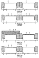
- FIG. 2a-2e A further prior art method of forming a dual gate oxide will be described in the following with reference to Figures 2a-2e.
- a substrate 1 with portions 2 and 3 on its upper surface.
- a thick layer of oxide 5 is formed on both portions 2 and 3, as depicted in Figure 2b; to this end, a common process, for instance a thermal oxidization process, may be carried out.
- the prior art method of document US-A-6087236 discloses the selective total etching of a first portion of an initial oxynitride and the regrowth of an oxynitride of a different thickness to replace it.
- the prior art method of document US-A-6033943 discloses the selective partial etching of a portion of an initial oxide layer and the growth of a second oxide on the same portion.
- the method includes thinning the initial layer of nitrided oxide on at least one first portion of the surface of the substrate to the respective, first predefined thickness. Additionally, the method comprises thinning the initial layer of nitrided oxide on at least one second portion of the surface of the substrate to the respective, second, predefined, different thickness.
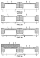
- the invention relates to a method of forming at least one first layer of nitrided oxide of a first, predefined thickness on at least one first portion of the surface of a substrate and at least one second layer of nitrided oxide of a second, predefined, different thickness on at least one second portion of the surface of the substrate.
- the method comprises thermally growing at least one layer of oxide in a nitrogen-containing atmosphere so as to form at least one initial layer of nitrided oxide of an initial thickness exceeding both the first and second predefined thickness on at least one first and one second portion of the surface of the substrate.
- the method includes thinning the initial layer of nitrided oxide on at least one first portion of the surface of the substrate to the respective, first predefined thickness, and thinning the initial layer of nitrided oxide on at least one second portion of the surface of the substrate to the respective, second, predefined, different thickness.
- the invention relates to a method of forming at least one first layer of oxide of a first, predefined thickness on at least one first portion of the surface of a substrate and at least one second layer of oxide of a second, predefined, different thickness on at least one second portion of the surface of the substrate, wherein the method comprises forming at least one initial layer of nitrided oxide of an initial thickness exceeding both the first and second predefined thickness on at least one first and one second portion of the surface of the substrate and thinning the initial layer of nitrided oxide on at least one first portion of the surface of the substrate to a first, intermediate thickness lower than the respective, first predefined thickness.
- the method includes thinning the initial layer of nitrided oxide on at least one second portion of the surface of the substrate to a second, intermediate thickness different from the first intermediate thickness and lower than the respective, second predefined thickness. Moreover a layer of oxide is added to the at least two layers of nitrided oxide so as to obtain at least two layers of oxide of predefined, different thicknesses.
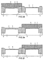
- a method of forming at least one first layer of oxide of a first, predefined thickness on at least one first portion of the surface of a substrate and at least one second layer of oxide of a second, predefined, different thickness on at least one second portion of the surface of the substrate comprises thermal growing at least one initial layer of oxide of an initial thickness exceeding both the first and second, predefined thickness on at least one first and one second portion of the surface of the substrate and annealing the initial layer of oxide in a nitrogen-containing atmosphere so as to form an initial layer of nitrided oxide on at least one first and one second portion of the surface of the substrate.
- the layer of nitrided oxide is removed from at least one first portion of the surface of the substrate targeted for the thin layer of oxide and the initial layer of nitrided oxide is thinned on at least one second portion of the surface of the substrate targeted for the thick layer of oxide to a thickness lower than the respective, predefined thickness.
- a layer of oxide is deposited on at least one first and second portion of the surface of the substrate so as to obtain at least two layers of oxide of predefined, different thicknesses.
- references 6 and 8 relate to corresponding layers of masking resist while reference 5 relates to an initial layer formed on both portions 2 and 3.
- references 7 and 9 relate to the final layers formed on the portions 3 and 2 of the substrate, respectively.
- references 7' and 9' relate to intermediate layers formed on the portions 3 and 2, respectively.
- the portion of the surface of the substrate targeted for the final, thick layer is masked, for instance by depositing a masking layer 6 of, for example, photoresist.
- Masking the portion 2 can be carried out according to methods well known in the art, including suitable photolithographic steps.
- the uncovered initial layer 5 on the portion 3 is thinned to a thickness corresponding to the final thickness of the layer 7.
- Thinning the layer 5 on portion 3 can be carried out by, for example, wet-etching the layer 5.
- the substrate may be immersed in an ammonium peroxide mixture for a predefined period of time, with the ammonium peroxide mixture having a predefined etching rate.
- the thickness of the final layer may essentially correspond to the predefined thickness.
- the masking layer 6 on portion 2 is then removed and a masking layer 8 of, for example, photoresist, is deposited on the portion 3.
- the uncovered initial layer 5 on portion 2 is then thinned (for instance by wet-etching) so as to obtain the second intermediate layer 9' of nitride oxide of an intermediate thickness lower than the final predefined thickness and differing from the thickness of the intermediate layer 7' (see Figure 4f).
- the initial layer 5 of nitrided oxide on portion 3 in this embodiment is simply removed, and there is no need of obtaining an intermediate layer of a predefined thickness, no particular measurements in this respect are required. Using this process flow, all that needs to be determined is that etching is performed for a period of time long enough to allow the substantially complete removal of the initial layer 5 on the portion 3. After the masking layer 6 is removed, the initial layer 5 on portion 2 is thinned so as to obtain the intermediate layer 9' of an intermediate thickness accommodating the desired final thickness difference between the final layer on portion 2 and the final layer on portion 3.
- a thickness difference of a few tenths of a nanometer (nm) is required, possibly within a strict tolerance, the intermediate thickness of the layer 9' must be defined accurately.
- a wet-etching process may be used, wherein the substrate is immersed in an etching mixture having a predefined etching rate during a predefined period of time.
- a method of forming layers of oxide of different thickness on the surface of a substrate which shows the following advantages with respect to prior art methods: (1) a limited number of masking steps is required; (2) very thin oxide layers, within the range of some tenths of a nanometer (nm) can be formed; (3) the thickness differences can be kept within the range of some tenths of a nanometer (nm); (4) no high temperature thermal oxidations are required; and (5) the process flow is compliant with the many sophisticated chemical vapor deposition techniques for gate dielectric deposition.
Landscapes
- Engineering & Computer Science (AREA)
- Microelectronics & Electronic Packaging (AREA)
- Power Engineering (AREA)
- Condensed Matter Physics & Semiconductors (AREA)
- General Physics & Mathematics (AREA)
- Physics & Mathematics (AREA)
- Computer Hardware Design (AREA)
- Manufacturing & Machinery (AREA)
- Chemical & Material Sciences (AREA)
- Chemical Kinetics & Catalysis (AREA)
- Crystallography & Structural Chemistry (AREA)
- General Chemical & Material Sciences (AREA)
- Ceramic Engineering (AREA)
- Formation Of Insulating Films (AREA)
- Metal-Oxide And Bipolar Metal-Oxide Semiconductor Integrated Circuits (AREA)
Claims (11)
- Verfahren zur Bildung zumindest einer ersten Schicht (7) aus stickstoffenthaltendem Oxid mit einer ersten vordefinierten Dicke auf zumindest einem ersten Bereich der Oberfläche eines Substrats (1) und zumindest einer zweiten Schicht (9) aus stickstoffenthaltendem Oxid mit einer zweiten vordefinierten unterschiedlichen Dicke auf zumindest einem zweiten Bereich der Oberfläche des Substrats (1), mit:Bilden zumindest einer Anfangsschicht (5) aus stickstoffenthaltendem Oxid mit einer Anfangsdicke, die größer als die erste und die zweite vordefinierte Dicke ist, auf zumindest einem ersten und einem zweiten Bereich der Oberfläche des Substrats (1);Dünnen der Anfangsschicht (5) aus stickstoffenthaltendem Oxid auf dem zumindest einen ersten Bereich der Oberfläche des Substrats auf die entsprechende erste vordefinierte Dicke; undDünnen der Anfangsschicht (5) aus stickstoffenthaltendem Oxid auf dem zumindest einen zweiten Bereich der Oberfläche des Substrats auf die entsprechende zweite vordefinierte unterschiedliche Dicke.
- Verfahren nach Anspruch 1, wobei das Dünnen der Anfangsschicht (5) aus stickstoffenthaltendem Oxid auf dem zumindest einen ersten und einen zweiten Bereich der Oberfläche des Substrats umfasst:Maskieren des zumindest einen ersten Bereichs der Oberfläche des Substrats (1) und Nassätzen der unbedeckten Anfangsschicht (5) aus stickstoffenthaltendem Oxid auf dem zumindest einen zweiten Bereich der Oberfläche des Substrats; undMaskieren des zumindest einen zweiten Bereichs der Oberfläche des Substrats (1) und Nassätzen der unbedeckten Anfangsschicht (5) aus stickstoffenthaltendem Oxid auf dem zumindest einen ersten Bereich der Oberfläche des Substrats.
- Verfahren nach Anspruch 2, wobei die Anfangsschicht (5) aus stickstoffenthaltendem Oxid nassgeätzt wird unter Anwendung einer Ammoniakperoxidmischung mit einer vordefinierten Ätzrate.
- Verfahren nach Anspruch 3, wobei die Anfangsschicht (5) auf dem zumindest einen ersten Bereich nassgeätzt wird für eine erste vordefinierte Zeitdauer und die Anfangsschicht auf dem zumindest einen zweiten Bereich nassgeätzt wird für eine zweite vordefinierte unterschiedliche Zeitdauer.
- Verfahren nach Anspruch 4, wobei die anfängliche Dicke der Anfangsschicht (5) aus stickstoffenthaltendem Oxid die erste und die zweite vordefinierte Dicke um ungefähr 10 bis 50 % übersteigt.
- Verfahren zur Bildung zumindest einer ersten Oxidschicht mit einer ersten vordefinierten Dicke auf zumindest einem ersten Bereich der Oberfläche eines Substrats (1) und zumindest einer zweiten Oxidschicht mit einer zweiten vordefinierten unterschiedlichen Dicke auf zumindest einem zweiten Bereich der Oberfläche des Substrats, mit:Bilden zumindest einer Anfangsschicht (5) aus stickstoffenthaltendem Oxid mit einer Anfangsdicke, die sowohl die erste als auch die zweite vordefinierte Dicke übersteigt, auf zumindest einem ersten und einem zweiten Bereich der Oberfläche des Substrats;Dünnen der Anfangsschicht (5) aus stickstoffenthaltendem Oxid auf dem zumindest einen ersten Bereich der Oberfläche des Substrats (1) auf eine erste Zwischendicke, die geringer als die entsprechende erste vordefinierte Dicke ist;Dünnen der Anfangsschicht (5) aus stickstoffenthaltendem Oxid auf dem zumindest einen zweiten Bereich der Oberfläche des Substrats (1) auf eine zweite Zwischendicke, die sich von der ersten Zwischendicke unterscheidet und die kleiner als die entsprechende zweite vordefinierte Dicke ist; undHinzufügen einer Oxidschicht zu den zumindest zwei Schichten aus stickstoffenthaltendem Oxid, um zumindest zwei Oxidschichten mit einer vordefinierten unterschiedlichen Dicke zu erhalten.
- Verfahren nach Anspruch 6, wobei die anfängliche Dicke der Anfangsschicht aus stickstoffenthaltendem Oxid die erste und die zweite vordefinierte Dicke um ungefähr 10 bis 50 % übersteigt.
- Verfahren zur Bildung zumindest einer ersten Oxidschicht mit einer ersten vordefinierten Dicke auf zumindest einem ersten Bereich der Oberfläche eines Substrats (1) und zumindest einer zweiten Oxidschicht mit einer zweiten vordefinierten unterschiedlichen Dicke auf zumindest einem zweiten Bereich der Oberfläche des Substrats (1), mit:thermisches Wachsen zumindest einer Oxidschicht in einer stickstoffenthaltenden Atmosphäre, um zumindest eine Anfangsschicht (5) aus stickstoffenthaltendem Oxid mit einer Anfangsdicke, die sowohl die erste als auch die zweite vordefinierte Dicke übersteigt, auf zumindest einem ersten und einem zweiten Bereich der Oberfläche des Substrats (1) zu bilden;Entfernen der Schicht (5) aus stickstoffenthaltendem Oxid von dem zumindest einen ersten Bereich der Oberfläche des Substrats, der für die dünne Oxidschicht vorgesehen ist;Dünnen der Anfangsschicht (5) aus stickstoffenthaltendem Oxid auf dem zumindest einen zweiten Bereich der Oberfläche des Substrats (1), der für die dicke Oxidschicht vorgesehen ist, auf eine Dicke, die geringer als die entsprechende vordefinierte Dicke ist; undthermisches Wachsen einer Oxidschicht auf dem zumindest einen ersten und einen zweiten Bereich der Oberfläche des Substrats (1), um zumindest zwei Oxidschichten mit vordefinierten unterschiedlichen Dicken zu erhalten.
- Verfahren nach Anspruch 8, wobei das Entfernen der Schicht (5) aus stickstoffenthaltendem Oxid von dem zumindest einen ersten Bereich der Oberfläche des Substrats (1), der für die dünne Oxidschicht vorgesehen ist, umfasst: Maskieren des zumindest einen zweiten Bereichs der Oberfläche des Substrats (1), der für die dicke Oxidschicht vorgesehen ist, und Trockenätzen oder Nassätzen der Schicht aus Oxid auf dem zumindest einen ersten Bereich der Oberfläche des Substrats (1), der für die dünne Oxidschicht vorgesehen ist.
- Verfahren nach Anspruch 8, wobei das Dünnen der Anfangsschicht (5) aus stickstoffenthaltendem Oxid auf dem zumindest einen zweiten Bereich der Oberfläche des Substrats (1), der für die dicke Oxidschicht vorgesehen ist, umfasst: Maskieren des zumindest einen ersten Bereichs der Oberfläche des Substrats (1), der für die dünne Oxidschicht vorgesehen ist, und Nassätzen der unbedeckten Anfangsschicht aus stickstoffenthaltendem Oxid auf dem zumindest einen zweiten Bereich der Oberfläche des Substrats (1), der für die dicke Oxidschicht vorgesehen ist.
- Verfahren nach Anspruch 8, wobei die anfängliche Dicke der Anfangsschicht (5) aus stickstoffenthaltendem Oxid die erste und die zweite vordefinierte Dicke um ungefähr 10 bis 50 % übersteigt.
Applications Claiming Priority (5)
| Application Number | Priority Date | Filing Date | Title |
|---|---|---|---|
| DE10207122 | 2002-02-20 | ||
| DE10207122A DE10207122B4 (de) | 2002-02-20 | 2002-02-20 | Ein Verfahren zur Herstellung von Schichten aus Oxid auf einer Oberfläche eines Substrats |
| US10/208,308 US6703278B2 (en) | 2002-02-20 | 2002-07-30 | Method of forming layers of oxide on a surface of a substrate |
| US208308 | 2002-07-30 | ||
| PCT/US2002/040807 WO2003073491A1 (en) | 2002-02-20 | 2002-12-20 | Method of forming layers of oxide of different thicknesses on a surface of a substrate |
Publications (2)
| Publication Number | Publication Date |
|---|---|
| EP1476899A1 EP1476899A1 (de) | 2004-11-17 |
| EP1476899B1 true EP1476899B1 (de) | 2007-03-07 |
Family
ID=27766671
Family Applications (1)
| Application Number | Title | Priority Date | Filing Date |
|---|---|---|---|
| EP02787067A Expired - Lifetime EP1476899B1 (de) | 2002-02-20 | 2002-12-20 | Verfahren zur herstellung von oxidschichten mit unterschiedlicher dicke auf einer substratoberfläche |
Country Status (6)
| Country | Link |
|---|---|
| EP (1) | EP1476899B1 (de) |
| JP (1) | JP4145802B2 (de) |
| CN (1) | CN1315162C (de) |
| AU (1) | AU2002351408A1 (de) |
| TW (1) | TWI278038B (de) |
| WO (1) | WO2003073491A1 (de) |
Families Citing this family (4)
| Publication number | Priority date | Publication date | Assignee | Title |
|---|---|---|---|---|
| KR100678321B1 (ko) | 2005-12-14 | 2007-02-02 | 동부일렉트로닉스 주식회사 | 서로 다른 두께의 게이트 유전층들을 형성하는 방법 |
| DE102017104906A1 (de) * | 2017-03-08 | 2018-09-13 | Olav Birlem | Anordnung und Verfahren zum Bereitstellen einer Vielzahl von Nanodrähten |
| CN108257860A (zh) * | 2018-01-19 | 2018-07-06 | 武汉新芯集成电路制造有限公司 | 一种栅极氧化层的制作方法 |
| CN114765107A (zh) * | 2021-01-14 | 2022-07-19 | 长鑫存储技术有限公司 | 半导体结构的制备方法及半导体结构 |
Family Cites Families (4)
| Publication number | Priority date | Publication date | Assignee | Title |
|---|---|---|---|---|
| US6033943A (en) * | 1996-08-23 | 2000-03-07 | Advanced Micro Devices, Inc. | Dual gate oxide thickness integrated circuit and process for making same |
| US6087236A (en) * | 1998-11-24 | 2000-07-11 | Intel Corporation | Integrated circuit with multiple gate dielectric structures |
| US6235590B1 (en) * | 1998-12-18 | 2001-05-22 | Lsi Logic Corporation | Fabrication of differential gate oxide thicknesses on a single integrated circuit chip |
| KR20010004417A (ko) * | 1999-06-28 | 2001-01-15 | 김영환 | 반도체장치의 듀얼 게이트산화막 형성 방법 |
-
2002
- 2002-12-20 WO PCT/US2002/040807 patent/WO2003073491A1/en active IP Right Grant
- 2002-12-20 EP EP02787067A patent/EP1476899B1/de not_active Expired - Lifetime
- 2002-12-20 CN CNB028281977A patent/CN1315162C/zh not_active Expired - Fee Related
- 2002-12-20 JP JP2003572081A patent/JP4145802B2/ja not_active Expired - Fee Related
- 2002-12-20 AU AU2002351408A patent/AU2002351408A1/en not_active Abandoned
-
2003
- 2003-02-19 TW TW092103374A patent/TWI278038B/zh not_active IP Right Cessation
Also Published As
| Publication number | Publication date |
|---|---|
| JP4145802B2 (ja) | 2008-09-03 |
| CN1620718A (zh) | 2005-05-25 |
| CN1315162C (zh) | 2007-05-09 |
| AU2002351408A1 (en) | 2003-09-09 |
| EP1476899A1 (de) | 2004-11-17 |
| JP2005518675A (ja) | 2005-06-23 |
| TWI278038B (en) | 2007-04-01 |
| TW200304187A (en) | 2003-09-16 |
| WO2003073491A1 (en) | 2003-09-04 |
Similar Documents
| Publication | Publication Date | Title |
|---|---|---|
| US8987081B2 (en) | Method of manufacturing semiconductor device with offset sidewall structure | |
| US6048769A (en) | CMOS integrated circuit having PMOS and NMOS devices with different gate dielectric layers | |
| US6080682A (en) | Methodology for achieving dual gate oxide thicknesses | |
| US6756635B2 (en) | Semiconductor substrate including multiple nitrided gate insulating films | |
| KR100400323B1 (ko) | 반도체 소자의 시모스(cmos) 및 그의 제조 방법 | |
| EP1711959B1 (de) | Transistor mit dotiertem gate-dielektrikum und verfahren zu seiner herstellung | |
| KR100757026B1 (ko) | 반도체 장치의 제조 방법 | |
| US20020130393A1 (en) | Semiconductor device and method of fabricating the same | |
| TWI400741B (zh) | 利用預置金屬介電質線性應力之高性能互補金氧半導體電晶體 | |
| US20060063316A1 (en) | Method for fabricating semiconductor device | |
| US20060138550A1 (en) | Semiconductor device with multiple gate dielectric layers and method for fabricating the same | |
| US7247914B2 (en) | Semiconductor device and method for fabricating the same | |
| US6703278B2 (en) | Method of forming layers of oxide on a surface of a substrate | |
| US20060249795A1 (en) | Semiconductor device and fabricating method thereof | |
| US7468297B2 (en) | Method of manufacturing semiconductor device | |
| US6667206B2 (en) | Method of manufacturing semiconductor device | |
| WO2007098459A2 (en) | Semiconductor device with nitrogen containing oxide layer | |
| EP1476899B1 (de) | Verfahren zur herstellung von oxidschichten mit unterschiedlicher dicke auf einer substratoberfläche | |
| KR20030091814A (ko) | 반도체 집적 회로 장치 및 그 제조 방법 | |
| US20040161934A1 (en) | Method for manufacturing semiconductor device | |
| JP2008066394A (ja) | 半導体装置およびその製造方法 | |
| JP2005252052A (ja) | 半導体装置及びその製造方法 | |
| JPH1131814A (ja) | 半導体装置の製造方法 | |
| US20050224857A1 (en) | MOS transistor | |
| JPH11163161A (ja) | 相補型mos半導体装置の製造方法 |
Legal Events
| Date | Code | Title | Description |
|---|---|---|---|
| PUAI | Public reference made under article 153(3) epc to a published international application that has entered the european phase |
Free format text: ORIGINAL CODE: 0009012 |
|
| 17P | Request for examination filed |
Effective date: 20040816 |
|
| AK | Designated contracting states |
Kind code of ref document: A1 Designated state(s): AT BE BG CH CY CZ DE DK EE ES FI FR GB GR IE IT LI LU MC NL PT SE SI SK TR |
|
| AX | Request for extension of the european patent |
Extension state: AL LT LV MK RO |
|
| RIN1 | Information on inventor provided before grant (corrected) |
Inventor name: WIECZOREK, KARSTEN Inventor name: KRUEGEL, STEPHAN Inventor name: GRAETSCH, FALK |
|
| GRAP | Despatch of communication of intention to grant a patent |
Free format text: ORIGINAL CODE: EPIDOSNIGR1 |
|
| GRAS | Grant fee paid |
Free format text: ORIGINAL CODE: EPIDOSNIGR3 |
|
| GRAA | (expected) grant |
Free format text: ORIGINAL CODE: 0009210 |
|
| AK | Designated contracting states |
Kind code of ref document: B1 Designated state(s): DE GB |
|
| REG | Reference to a national code |
Ref country code: GB Ref legal event code: FG4D |
|
| REF | Corresponds to: |
Ref document number: 60218750 Country of ref document: DE Date of ref document: 20070419 Kind code of ref document: P |
|
| PLBE | No opposition filed within time limit |
Free format text: ORIGINAL CODE: 0009261 |
|
| STAA | Information on the status of an ep patent application or granted ep patent |
Free format text: STATUS: NO OPPOSITION FILED WITHIN TIME LIMIT |
|
| 26N | No opposition filed |
Effective date: 20071210 |
|
| REG | Reference to a national code |
Ref country code: GB Ref legal event code: 732E Free format text: REGISTERED BETWEEN 20091119 AND 20091125 |
|
| PGFP | Annual fee paid to national office [announced via postgrant information from national office to epo] |
Ref country code: GB Payment date: 20101123 Year of fee payment: 9 |
|
| PGFP | Annual fee paid to national office [announced via postgrant information from national office to epo] |
Ref country code: DE Payment date: 20101230 Year of fee payment: 9 |
|
| GBPC | Gb: european patent ceased through non-payment of renewal fee |
Effective date: 20111220 |
|
| PG25 | Lapsed in a contracting state [announced via postgrant information from national office to epo] |
Ref country code: GB Free format text: LAPSE BECAUSE OF NON-PAYMENT OF DUE FEES Effective date: 20111220 |
|
| REG | Reference to a national code |
Ref country code: DE Ref legal event code: R119 Ref document number: 60218750 Country of ref document: DE Effective date: 20130702 |
|
| PG25 | Lapsed in a contracting state [announced via postgrant information from national office to epo] |
Ref country code: DE Free format text: LAPSE BECAUSE OF NON-PAYMENT OF DUE FEES Effective date: 20130702 |