EP1471633A2 - Radioempfänger und Verfahren zur Radiosignalverarbeitung - Google Patents
Radioempfänger und Verfahren zur Radiosignalverarbeitung Download PDFInfo
- Publication number
- EP1471633A2 EP1471633A2 EP04251939A EP04251939A EP1471633A2 EP 1471633 A2 EP1471633 A2 EP 1471633A2 EP 04251939 A EP04251939 A EP 04251939A EP 04251939 A EP04251939 A EP 04251939A EP 1471633 A2 EP1471633 A2 EP 1471633A2
- Authority
- EP
- European Patent Office
- Prior art keywords
- gain
- amplifier
- change
- changed
- signal
- Prior art date
- Legal status (The legal status is an assumption and is not a legal conclusion. Google has not performed a legal analysis and makes no representation as to the accuracy of the status listed.)
- Withdrawn
Links
Images


Classifications
-
- H—ELECTRICITY
- H04—ELECTRIC COMMUNICATION TECHNIQUE
- H04B—TRANSMISSION
- H04B1/00—Details of transmission systems, not covered by a single one of groups H04B3/00 - H04B13/00; Details of transmission systems not characterised by the medium used for transmission
- H04B1/06—Receivers
- H04B1/10—Means associated with receiver for limiting or suppressing noise or interference
-
- H—ELECTRICITY
- H03—ELECTRONIC CIRCUITRY
- H03G—CONTROL OF AMPLIFICATION
- H03G3/00—Gain control in amplifiers or frequency changers
- H03G3/20—Automatic control
- H03G3/30—Automatic control in amplifiers having semiconductor devices
- H03G3/3052—Automatic control in amplifiers having semiconductor devices in bandpass amplifiers (H.F. or I.F.) or in frequency-changers used in a (super)heterodyne receiver
- H03G3/3068—Circuits generating control signals for both R.F. and I.F. stages
-
- H—ELECTRICITY
- H03—ELECTRONIC CIRCUITRY
- H03D—DEMODULATION OR TRANSFERENCE OF MODULATION FROM ONE CARRIER TO ANOTHER
- H03D3/00—Demodulation of angle-, frequency- or phase- modulated oscillations
- H03D3/007—Demodulation of angle-, frequency- or phase- modulated oscillations by converting the oscillations into two quadrature related signals
- H03D3/008—Compensating DC offsets
-
- H—ELECTRICITY
- H04—ELECTRIC COMMUNICATION TECHNIQUE
- H04B—TRANSMISSION
- H04B1/00—Details of transmission systems, not covered by a single one of groups H04B3/00 - H04B13/00; Details of transmission systems not characterised by the medium used for transmission
- H04B1/06—Receivers
- H04B1/16—Circuits
- H04B1/30—Circuits for homodyne or synchrodyne receivers
-
- H—ELECTRICITY
- H04—ELECTRIC COMMUNICATION TECHNIQUE
- H04L—TRANSMISSION OF DIGITAL INFORMATION, e.g. TELEGRAPHIC COMMUNICATION
- H04L27/00—Modulated-carrier systems
- H04L27/32—Carrier systems characterised by combinations of two or more of the types covered by groups H04L27/02, H04L27/10, H04L27/18 or H04L27/26
- H04L27/34—Amplitude- and phase-modulated carrier systems, e.g. quadrature-amplitude modulated carrier systems
- H04L27/38—Demodulator circuits; Receiver circuits
- H04L27/3809—Amplitude regulation arrangements
Definitions
- the present invention relates to a radio receiver and a radio signal processing method.
- radio communication devices have widely spread. As a result, it is increasingly demanded to reduce the number of components and the manufacture cost for a radio circuit and manufacture the radio circuit as a monolithic IC. In order to cope with this demand, the direct conversion scheme is adopted for the radio circuits.
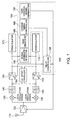
- Fig. 8 is a block diagram of a conventional receiver adopting the direct conversion scheme.
- An antenna 10 receives an RF (Radio Frequency) signal, and an LNA (Low Noise Amplifier) 20 amplifies this RF signal.
- a quadrature demodulator 30 multiplies the amplified RF signal by an LO (Local Oscillator)signal supplied from a local oscillator (not illustrated). As a result, the RF signal is directly converted to a baseband signal.
- An LPF (Low Pass Filer) 40 conducts waveform shaping on the baseband signal, and a VGA (Variable Gain Amplifier) 50 amplifies this baseband signal.
- a demodulator 70 demodulates this baseband signal to a digital signal. In this way, the receiver using the direct conversion scheme converts the RF signal to a digital signal, and then demodulates it by using digital signal processing.
- the baseband signal amplified by the VGA 50 is input not only to the demodulator 70 but also to a gain controller 60 and a DC offset canceller 94.
- a signal strength detector 80 measures the strength of the baseband signal.
- a gain selector 90 decides whether to switch the gain of the LNA 20 and the gain of the VGA 50 on the basis of the measured value of the baseband signal.
- a gain control signal generator 92 outputs a gain control signal to the LNA 20 and the VGA 50 to switch the gain in accordance with the decision made by the gain selector 90. In this way, the gain controller 60 effects feedback control on the strength of the baseband signal.
- the DC (Direct Current) offset canceller 94 removes a DC offset component from the baseband signal amplified by the VGA 50, and feeds back this to the VGA 50.
- problems concerning the DC offset component are described in "Research development tendency of mixer for direct conversion receiver ("Mission Impossible ? A Review of Mixers for Direct-Conversion Receivers”)” written by Hiroshi Tanimoto, The Transactions of the Institute of Electronics, Information, and Communication Engineers, section C, Vol.J84-C, No.5, pp. 337-348, May 2001.
- Figs. 9A and 9B are graphs showing gains of the LNA 20 and the VGA 50, respectively.
- Fig. 9C is a graph showing a transient response component of a DC offset in the output of the VGA 50. The gains of the LNA 20 and the VGA 50 are simultaneously switched.
- the VGA 50 is switched simultaneously from a low gain to a high gain. In some cases, therefore, DC offsets of both the LNA 20 and the VGA50 overlap each other, and a very large transient response component occurs, resulting in a degraded reception performance. This is because the LNA 20 is disposed in a stage in the radio circuit preceding the VGA 50, and consequently the transient response component of the DC offset generated in the LNA 20 is amplified by the high gain obtained after the change in the VGA 50.
- An advantage of an aspect of the present invention is to provide a radio receiver of direct conversion scheme in which degradation of the reception performance caused by the transient response component of the DC offset is suppressed.
- a radio receiver of an embodiment accordance with the instant invention comprises a first amplifier to amplify a received radio signal; a demodulation circuit line comprising a quadrature demodulator to demodulate the radio signal amplified by said first amplifier and to generate a baseband signal, a second amplifier to amplify the baseband signal , and a demodulator to demodulate the baseband signal amplified by said second amplifier; and a gain controller to control timing of a change in a gain of said second amplifier, in case that the gain of said first amplifier and the gain of said second amplifier are changed, on the basis of a gain of said first amplifier before and after the change.
- a radio receiver of another embodiment accordance with the instant invention comprises a radio receiver comprising: a first amplifier to amplify a received radio signal; a quadrature demodulator to demodulate the radio signal amplified by said first amplifier and to generate a baseband signal; a second amplifier to amplify, after changing a gain of said first amplifier, the baseband signal with a gain based on a gain of said first amplifier obtained before and after the change; and a demodulator to demodulate the baseband signal amplified by said second amplifier.
- a radio receiver of further embodiment accordance with the instant invention comprises a first amplifier to amplify a received radio signal; a quadrature demodulator to demodulate the radio signal amplified by said first amplifier and to generate a baseband signal; a second amplifier to amplify the baseband signal; a demodulator to demodulate the baseband signal amplified by said second amplifier; and a gain controller to delay timing of a change in a gain of said second amplifier as compared with timing of a change in a gain of said first amplifier, in case that the gain of said first amplifier is changed from a high gain to a low gain and the gain of said second amplifier is changed from a low gain to a high gain.
- a radio signal processing method of an embodiment accordance with the instant invention comprises: receiving a radio signal; amplifying the radio signal; demodulating the amplified radio signal to a baseband signal; amplifying the baseband signal; demodulating the amplified baseband signal; determining timing of a change in a gain of said first amplifier and a gain of said second amplifier, in case that the gain of said first amplifier and the gain of said second amplifier are changed, on the basis of the gain of said first amplifier obtained before and after the change; and changing the gain of said first amplifier and the gain of said second amplifier in accordance with the determined timing.
- the gain of the LNA and the gain of the VGA can be changed respectively at points in time that are different from each other. As a result, the transient response component of the DC offset in the output of the VGA is reduced.
- Fig. 1 is a block diagram of a radio receiver 100 according to an embodiment of the present invention.
- the radio receiver 100 is a radio receiver using the direct conversion scheme.
- the direct conversion scheme is a scheme in which an RF signal having a high frequency is converted to a baseband signal having a low frequency without using an intermediate frequency.
- the radio receiver 100 includes an antenna 110, an LNA 120, a quadrature demodulator 130, an LPF 140, a VGA 150, a gain controller 160, a demodulator 170 and a DC offset canceller 194.
- the DC offset canceller 194 is, for example, a circuit formed by connecting an amplifier having a constant gain and an integrator (low pass filter) in cascade. Owing to such a configuration, the DC offset canceller 194 can remove the DC offset component.
- the DC offset canceller 194 removes a DC offset component contained in the baseband signal, and then feeds back this baseband signal to the VGA 150.
- the DC offset component is induced by a component of an LO signal that leaks to the antenna 110 and the LNA 120 and undergoes frequency conversion as an input of the quadrature demodulator 130.
- Each of the LNA 120 and the VGA 150 is formed so as to be able to be changed stepwise in gain.
- the gain of the LNA 120 can be changed to two levels, i.e. , a high-gain level and a low-gain level.
- the gain of the VGA 150 can be changed to multiple levels between a high gain and a low gain inclusive thereof.
- the gain controller 160 is formed so as to effect feedback control on the gains of the LNA 120 and the VGA 150 in order to keep a baseband signal supplied from the VGA 150 at a predetermined signal strength.
- the gain controller 160 includes a signal strength detector 180, a gain selector 190, a change timing controller 196, a gain control signal generator 192 and a delay controller 198.
- the signal strength detector 180 detects the signal strength of the baseband signal amplified by the VGA 150.
- the gain selector 190 conducts selection on the gain of the LNA 120 and the gain of the VGA 150 so as to keep the signal strength of the baseband signal detected by the signal strength detector 180 at a constant signal strength.
- the change timing controller 196 controls timing at which the gain of the VGA 150 should be changed, on the basis of the gain of the LNA 120 selected by the gain selector 190 and the actual gain of the LNA 120 at the current point in time.
- the quadrature demodulator 130, the VGA 150 and the demodulator 170 are connected in series.
- this is referred to as a demodulation circuit line.
- two demodulation circuit lines are connected in parallel after the LNA 120, and used for an I-axis component and a Q-axis component of a received signal, respectively.
- One gain controller 160 is connected to the two demodulation circuit lines to control the two VGAs 150 in common.
- the gain controller 160 changes gains of the two VGAs 150 by the same period of time after changing the gain of the LNA 120.
- the gain controller 160 changes gains of the two VGAs 150 by the same quantity. In this way, the gain controller 160 controls a plurality of demodulation circuit lines in common.
- the radio receiver 100 can demodulate the I-axis component and the Q-axis component of the received signal in common.
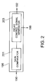
- Fig. 2 shows a concrete example of the change timing controller 196.
- the change timing controller 196 includes a gain comparator 201 and a delay control signal generator 203.
- the gain comparator 201 compares the actual gain of the LNA 120 at the current point in time with the gain of the LNA 120 selected by the gain selector 190.
- the gain comparator 201 previously stores a certain threshold concerning the gain of the LNA 120.
- the high gain of the LNA 120 is a gain larger than the threshold, and the low gain is a gain smaller than the threshold.
- the gain comparator 201 compares the gain of the LNA 120 before a change with the gain of the LNA 120 after the change. Then, with the comparison result, the gain comparator 201 decides whether the gain of the LNA 120 is changed from the high gain to the low gain, the gain of the LNA 120 is changed from the low gain to the high gain, or the gain of the LNA 120 is not changed.
- the gain of the LNA 120 before the change means the actual gain of the LNA 120 at the current point in time
- the gain of the LNA 120 after the change means the gain of the LNA 120 selected by the gain selector 190.
- changing the gain means switching the gain stepwise.
- the gain comparator 201 also previously stores a certain threshold concerning the gain of the VGA 150. The high gain of the VGA 150 is a gain larger than the threshold, and the low gain of the VGA 150 is a gain smaller than the threshold.
- the delay control signal generator 203 generates a delay control signal that indicates a delay time used to delay the change in gain of the VGA 150.
- the delay control signal generator 203 In the case where the gain of the LNA 120 is changed from the high gain to the low gain, the delay control signal generator 203 generates a delay control signal when the gain of the VGA 150 is changed from the low gain to the high gain. This delay control signal is output to the delay controller 198.
- the delay control signal generator 203 does not generate the delay control signal when the gain of the VGA 150 is changed.
- the gain control signal generator 192 is supplied with the gain selected in the gain selector 190 via the change timing controller 196.
- the gain control signal generator 192 outputs a gain control signal to the LNA 120 and the delay controller 198 on the basis of the gains of the LNA 120 and the VGA 150 selected by the gain selector 190.
- the gain control signal is a signal indicating the gains respectively of the LNA 120 and the VGA 150 selected by the gain selector 190.
- the delay controller 198 outputs the gain control signal to the VGA 150, after a predetermined delay time has elapsed since a point in time at which the delay controller 198 receives the gain control signal, in accordance with the delay control signal. Since the gain control signal is transmitted directly to the LNA 120, the gain of the VGA 150 is changed with a delay to the gain of the LNA 120. On the other hand, in the case where the delay control signal is not output from the delay control signal generator 203, the delay controller 198 outputs the gain control signal to the VGA 150 without delaying the gain control signal.
- the gain controller 160 is formed so as to control the timing at which the gain of the VGA 150 is changed on the basis of the gain of the LNA 120 before and after the change.
- the timing at which the gain of the VGA 150 is changed is controlled on the basis of the gain of the LNA 120 before and after the change.
- the timing at which the gain of the VGA 150 is changed may be controlled on the basis of the gains of the LNA 120 and the VGA 150 before and after the change.
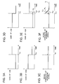
- Figs. 3A to 3F are time charts showing gains of the LNA 120 and the VGA 150, and the signal strength of the baseband signal. With reference to Figs. 3A to 3F, operation of the LNA 120 and the VGA 150 will now be described in further detail.
- the gain of the LNA 120 is changed from the low gain to the high gain as shown in Fig. 3A, and the gain of the VGA 150 is changed from the high gain to the low gain as shown in Fig. 3B.
- the gains of the LNA 120 and the VGA 150 are changed at a point in time t 20 .
- a transient response characteristic of the DC offset induced at this time is relatively small as shown in Fig. 3C.
- the gain of the LNA 120 is changed from the high gain to the low gain as shown in Fig. 3D, and the gain of the VGA 150 is changed from the low gain to the high gain as shown in Fig. 3E.
- the gain of the LNA 120 is changed at a point in time t 21 . If at this time the gain of the VGA 150 is changed simultaneously with the change in the gain of the LNA 120 as represented by a broken line in Fig. 3E, a large transient response component of the DC offset is induced as represented by a broken line in Fig. 3F.
- the gain of the VGA 150 is changed from the low gain to the high gain with a delay time Td after the change in the gain of the LNA 120 as represented by a solid line in Fig. 3E.
- the delay time Td is larger than 0, and smaller than a repetition period ( ⁇ t shown in Fig. 9) of the change in gains of the LNA 120 and the VGA 150.
- the gain of the VGA 150 is changed with a delay to the change in the gain of the LNA 120, in the present embodiment. Therefore, the transient response component of the DC offset can be reduced.
- an area S B of a region surrounded by a straight line L and the solid line is obviously smaller than an area S A of a region surrounded by the straight line L and the broken line.
- the DC offset component per unit time is smaller than that in the conventional technique. Since, as described above, the error rate in the reception characteristics is proportionate to an accumulation value of an area S per unit time, the present embodiment has a smaller error rate in the reception performance than that of the conventional technique. In the present embodiment, therefore, the reception performance becomes better than that in the conventional technique.
- the gain of the LNA 120 can be changed to two levels, it is also permissible that the gain of the LNA can be changed to three or more levels.
- Figs. 4A to 4H are time charts showing gains of the LNA 120 and VGA 150 in the case where the received electric field strength (so called "RSSI (received signal strength indicator))changes monotonously, and time charts showing signal strengths of the received signal and signal strengths of the baseband signal.
- RSSI received electric field strength indicator
- the gain of the VGA 150 there is an upper limit in the gain of the VGA 150. If the gain of the VGA 150 arrives at a vicinity of its upper limit at the point in time t 20 , therefore, the gain of the LNA 120 is changed from the low gain to the high gain as shown in Fig. 4B, and the gain of the VGA 150 is changed from the high gain to the low gain as shown in Fig. 4C.
- the gain change widths of the LNA 120 and the VGA 150 are nearly equal to each other. As a result, the fall in the gain of the VGA 150 can be compensated by the increase in the gain of the LNA 120.
- the transient response characteristic of the DC offset induced at this time is relatively small as shown in Fig. 4D.
- the gain of the VGA 150 is changed in a larger number of steps as compared with the gain of the LNA 120 as shown in Figs. 4B, 4C, 4F and 4G. Even if the received signal strength changes linearly as shown in Fig. 4A, therefore, the signal strength of the baseband signal can be kept constant in the present embodiment.
- the signal strength of the received signal further continues to fall.
- the signal strength of the baseband signal can be kept constant by making the gain of the VGA 150 further rise stepwise.
- the transient response component of the DC offset caused by the stepwise gain switching of the VGA 150 is omitted, because it is small.
- the gain of the VGA 150 arrives at a vicinity of its lower limit at the point in time t 21 , therefore, the gain of the LNA 120 is changed from the high gain to the low gain as shown in Fig. 4F. If at this time the gain of the VGA 150 is changed simultaneously with the change in the gain of the LNA 120, a large transient response component of the DC offset occurs at the point in time t 21 as represented by a broken line in Fig. 4H.
- the gain of the VGA 150 is changed from the low gain to the high gain with a delay time Td after the change in the gain of the LNA 120 as represented by a solid line in Fig. 4G.
- Td t 31 - t 21 .
- the delay time Td is a value that is larger than 0 and that is smaller than a repetition period ( ⁇ t shown in Fig. 9) of the change in gains of the LNA 120 and the VGA 150.
- the signal strength of the received signal further continues to rise.
- the signal strength of the baseband signal can be kept constant by making the gain of the VGA 150 fall gradually.
- the gain of the VGA 150 is changed with a delay to the change in the gain of the LNA 120, and consequently effects similar to those of the embodiment shown in Figs. 3A to 3F can be obtained.
- the gain of the VGA 150 is changed between the points in time t 21 and t 31 as represented by a broken line in Fig. 4G. This means that the gain of the VGA 150 is being controlled when the transient response component of the DC offset is occurring. Therefore, the gain of the VGA 150 is changed largely at the point in time t 21 .
- the gain of the VGA 150 is not changed during the delay time Td, i.e. , between the points in time t 21 and t 31 .
- the width of the gain of the VGA 150 changed at the point in time t 31 in the present variant is smaller than that at the point in time t 21 in the conventional technique. Therefore, the transient response component of the DC offset induced in the present variant is relatively small.
- the width of the gain of the VGA 150 changed at the point in time t 31 is equal to that changed at the point in time t 21 in the conventional technique.
- a peak P 2 of the transient response component of the DC offset induced at the point in time t 31 in the present variant becomes further smaller than a peak P 1 of the transient response component induced at the point in time t 31 in the embodiment shown in Figs. 3A to 3F.
- the gain of the VGA 150 is changed singly without changing the gain of the LNA 120 in some cases.
- the transient response component of the DC offset is relatively small similarly as in Fig. 4D, and consequently no problems are posed.
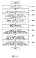
- Fig. 5 is a flow diagram showing operation of the radio receiver 100 in the embodiment.
- An RF signal is received by the antenna 110 (S10).
- the received signal is amplified by the LNA 120 (S20).
- the quadrature demodulator 130 converts the RF signal having a high frequency to the baseband signal (S30).
- the baseband signal is subjected to waveform shaping in the LPF 140 (S40), and amplified in the VGA 150 (S50).
- the DC offset canceller 194 removes the DC offset component from this baseband signal (S60).
- the gain controller 160 is supplied with the baseband signal output from the VGA 150, and the gain controller 160 effects feedback control on the LNA 120 and the VGA 150 (S70).
- the demodulator 170 demodulates the baseband signal to the digital signal (S80) .
- Fig. 6 is a flow diagram showing details of operation conducted by the gain controller 160 at the step S70. If the baseband signal is input to the gain controller 160, the signal strength detector 180 detects the signal strength of the baseband signal (S70-1).
- the gain selector 190 selects gains of the LNA 120 and the VGA 150 so as to keep the signal strength of the baseband signal constant (S70-3).
- the change timing controller 196 compares the actual gain state of the LNA 120 at the current point in time with the selected gain of the LNA 120 (S70-5) . As a result of this comparison, it is determined whether the gain of the LNA 120 passes through a threshold previously stored in the change timing controller 196 before and after a change (S70-6).
- the change timing controller 196 furthermore judges the gain state of the LNA 120 at the current point in time (S70-7). Judgment on the gain state of the LNA 120 can be conducted by determining whether the gain of the LNA 120 is higher than this threshold (S70-8) . If the gain of the LNA 120 at the current point in time is the high gain as a result of this decision, the change timing controller 196 outputs the delay control signal to the delay controller 198 (S70-9).
- the gain control signal generator 192 outputs the gain control signal to the LNA 120 and the delay controller 198 on the basis of the gains of the LNA 120 and the VGA 150 selected by the gain selector 190 (S70-11) .
- the delay controller 198 is supplied with the gain control signal and the delay control signal, and the delay controller 198 delays the gain control signal and outputs the delayed gain control signal to the VGA 150.
- the gain of the VGA 150 is changed with a delay to the change in the gain of the LNA 120 (S70-13).
- the change timing controller 196 does not output the delay control signal. Since the delay control signal is not output, the delay controller 198 outputs the gain control signal to the VGA 150 without delaying it. As a result, the gain of the VGA 150 is changed simultaneously with a change in the gain of the LNA 120 (S70-15).
- the change timing controller 196 further makes a decision whether to change the gain of the VGA 150 (S70-17). In this decision, the gain comparator 201 previously stores a threshold located between the low gain and the high gain of the VGA 150, and judges a gain higher than the threshold to be the high gain and judges gain lower than the threshold to be the low gain. If the gain of the VGA 150 passes through this threshold before and after the change, the change timing controller 196 decides to change the gain of the VGA 150 (S70-18).
- the gain control signal generator 192 outputs the gain control signal to the VGA 150 via the delay controller 198 to change the gain of the VGA 150. Since the delay control signal is not issued from the change timing controller 196, the delay controller 198 passes the gain control signal to the VGA 150 without delaying it. As a result, the gain of the VGA 150 is changed (S70-19).
- the delay controller 198 does not change the gain of VGA 150.
- Fig. 7 is a graph showing a DC offset component actually measured when the gain of the LNA 120 is changed from the high gain to the low gain and the gain of the VGA 150 is changed from the low gain to the high gain.
- Fig. 7 corresponds to the graph shown in Fig. 4H in which the signal strength of the baseband signal has been obtained by actually measuring it.
- a curve A shows a DC offset component measured when the gain of the LNA 120 and the gain of the VGA 150 are changed simultaneously in the same way as the conventional technique.
- a curve B shows a DC offset component measured when the gain of the VGA 150 is changed with a delay to a change in the gain of the LNA 120 according to the embodiment.
- the transient response component of the DC offset output from the VGA 150 is approximately 70 mV maximum.
- the transient response component of the DC offset output from the VGA 150 is approximately 30 mV maximum. Therefore, the transient response component in the curve B is obviously lower than the transient response component in the curve A.
- the probability in the embodiment that the DC offset component exceeds the threshold becomes lower as compared with the conventional technique.
- An area S B of a region surrounded by a curve B and a broken line is obviously smaller than an area S A of a region surrounded by a curve A and the broken line.
- the DC offset component per unit time is smaller as compared with the conventional technique. Since the error rate in the reception characteristic is proportionate to the accumulation value of the area S per unit time as described earlier, the error rate in the reception characteristic in the embodiment is smaller as compared with the conventional technique. As a result, the embodiment becomes better in reception performance than the conventional technique.
Landscapes
- Engineering & Computer Science (AREA)
- Computer Networks & Wireless Communication (AREA)
- Signal Processing (AREA)
- Power Engineering (AREA)
- Circuits Of Receivers In General (AREA)
- Control Of Amplification And Gain Control (AREA)
Applications Claiming Priority (2)
| Application Number | Priority Date | Filing Date | Title |
|---|---|---|---|
| JP2003122316 | 2003-04-25 | ||
| JP2003122316A JP3906179B2 (ja) | 2003-04-25 | 2003-04-25 | 無線受信機および無線信号処理方法 |
Publications (2)
| Publication Number | Publication Date |
|---|---|
| EP1471633A2 true EP1471633A2 (de) | 2004-10-27 |
| EP1471633A3 EP1471633A3 (de) | 2007-09-05 |
Family
ID=32959712
Family Applications (1)
| Application Number | Title | Priority Date | Filing Date |
|---|---|---|---|
| EP04251939A Withdrawn EP1471633A3 (de) | 2003-04-25 | 2004-03-31 | Radioempfänger und Verfahren zur Radiosignalverarbeitung |
Country Status (5)
| Country | Link |
|---|---|
| US (2) | US7245894B2 (de) |
| EP (1) | EP1471633A3 (de) |
| JP (1) | JP3906179B2 (de) |
| KR (1) | KR100615022B1 (de) |
| CN (1) | CN100359810C (de) |
Cited By (1)
| Publication number | Priority date | Publication date | Assignee | Title |
|---|---|---|---|---|
| GB2424326A (en) * | 2005-03-18 | 2006-09-20 | Motorola Inc | Direct conversion FM receiver employing average DC offset correction |
Families Citing this family (56)
| Publication number | Priority date | Publication date | Assignee | Title |
|---|---|---|---|---|
| JP3852919B2 (ja) * | 2001-12-25 | 2006-12-06 | 株式会社東芝 | 無線受信機 |
| JP3906179B2 (ja) * | 2003-04-25 | 2007-04-18 | 株式会社東芝 | 無線受信機および無線信号処理方法 |
| DE102004024875B4 (de) * | 2004-05-19 | 2006-09-07 | Infineon Technologies Ag | Verstärkeranordnung und Verfahren zur Kompensation eines Signalanteils in einer Verstärkeranordnung |
| US20080178692A1 (en) * | 2007-01-29 | 2008-07-31 | Searete Llc, A Limited Liability Corporation Of The State Of Delaware | Fluidic methods |
| US8340944B2 (en) | 2005-11-30 | 2012-12-25 | The Invention Science Fund I, Llc | Computational and/or control systems and methods related to nutraceutical agent selection and dosing |
| US10296720B2 (en) | 2005-11-30 | 2019-05-21 | Gearbox Llc | Computational systems and methods related to nutraceuticals |
| US20080103746A1 (en) | 2005-11-30 | 2008-05-01 | Searete Llc, A Limited Liability Corporation | Systems and methods for pathogen detection and response |
| US7827042B2 (en) | 2005-11-30 | 2010-11-02 | The Invention Science Fund I, Inc | Methods and systems related to transmission of nutraceutical associated information |
| US20080241909A1 (en) * | 2007-03-27 | 2008-10-02 | Searete Llc, A Limited Liability Corporation Of The State Of Delaware | Microfluidic chips for pathogen detection |
| US20080179255A1 (en) * | 2007-01-29 | 2008-07-31 | Searete Llc, A Limited Liability Corporation Of The State Of Delaware | Fluidic devices |
| US20080241910A1 (en) * | 2007-03-27 | 2008-10-02 | Searete Llc, A Limited Liability Corporation Of The State Of Delaware | Devices for pathogen detection |
| US7927787B2 (en) | 2006-06-28 | 2011-04-19 | The Invention Science Fund I, Llc | Methods and systems for analysis of nutraceutical associated components |
| US8000981B2 (en) | 2005-11-30 | 2011-08-16 | The Invention Science Fund I, Llc | Methods and systems related to receiving nutraceutical associated information |
| US7974856B2 (en) | 2005-11-30 | 2011-07-05 | The Invention Science Fund I, Llc | Computational systems and methods related to nutraceuticals |
| US8297028B2 (en) | 2006-06-14 | 2012-10-30 | The Invention Science Fund I, Llc | Individualized pharmaceutical selection and packaging |
| JP2008011027A (ja) * | 2006-06-28 | 2008-01-17 | Fujitsu Ltd | 受信装置 |
| US8221690B2 (en) * | 2007-10-30 | 2012-07-17 | The Invention Science Fund I, Llc | Systems and devices that utilize photolyzable nitric oxide donors |
| US20110190604A1 (en) * | 2006-12-22 | 2011-08-04 | Hyde Roderick A | Nitric oxide sensors and systems |
| US20090110933A1 (en) * | 2007-10-30 | 2009-04-30 | Searete Llc, A Limited Liability Corporation Of The State Of Delaware | Systems and devices related to nitric oxide releasing materials |
| US8642093B2 (en) * | 2007-10-30 | 2014-02-04 | The Invention Science Fund I, Llc | Methods and systems for use of photolyzable nitric oxide donors |
| US7862598B2 (en) * | 2007-10-30 | 2011-01-04 | The Invention Science Fund I, Llc | Devices and systems that deliver nitric oxide |
| US7975699B2 (en) | 2007-10-30 | 2011-07-12 | The Invention Science Fund I, Llc | Condoms configured to facilitate release of nitric oxide |
| JP4734262B2 (ja) * | 2007-01-26 | 2011-07-27 | 株式会社東芝 | 受信装置、無線装置、オフセットキャンセル方法 |
| US20080180259A1 (en) * | 2007-01-29 | 2008-07-31 | Searete Llc, A Limited Liability Corporation Of The State Of Delaware | Devices for allergen detection |
| US8617903B2 (en) * | 2007-01-29 | 2013-12-31 | The Invention Science Fund I, Llc | Methods for allergen detection |
| US20080181821A1 (en) * | 2007-01-29 | 2008-07-31 | Searete Llc, A Limited Liability Corporation Of The State Of Delaware | Microfluidic chips for allergen detection |
| US20090050569A1 (en) * | 2007-01-29 | 2009-02-26 | Searete Llc, A Limited Liability Corporation Of The State Of Delaware | Fluidic methods |
| US20080245740A1 (en) * | 2007-01-29 | 2008-10-09 | Searete Llc, A Limited Liability Corporation Of The State Of Delaware | Fluidic methods |
| US20080181816A1 (en) * | 2007-01-29 | 2008-07-31 | Searete Llc, A Limited Liability Corporation | Systems for allergen detection |
| US10001496B2 (en) | 2007-01-29 | 2018-06-19 | Gearbox, Llc | Systems for allergen detection |
| JP2008205956A (ja) * | 2007-02-21 | 2008-09-04 | Toshiba Corp | 受信装置、無線装置、オフセットキャンセル方法 |
| US20090215157A1 (en) * | 2007-03-27 | 2009-08-27 | Searete Llc | Methods for pathogen detection |
| US7817750B2 (en) * | 2007-05-21 | 2010-10-19 | Seiko Epson Corporation | Radio receiver including a delay-locked loop (DLL) for phase adjustment |
| US20090058531A1 (en) * | 2007-08-31 | 2009-03-05 | Nanoamp Solutions Inc. (Cayman) | Variable gain amplifier |
| US8877508B2 (en) * | 2007-10-30 | 2014-11-04 | The Invention Science Fund I, Llc | Devices and systems that deliver nitric oxide |
| US10080823B2 (en) | 2007-10-30 | 2018-09-25 | Gearbox Llc | Substrates for nitric oxide releasing devices |
| US20090112055A1 (en) * | 2007-10-30 | 2009-04-30 | Searete Llc, A Limited Liability Corporation Of The State Of Delaware | Sleeves configured to facilitate release of nitric oxide |
| US8980332B2 (en) | 2007-10-30 | 2015-03-17 | The Invention Science Fund I, Llc | Methods and systems for use of photolyzable nitric oxide donors |
| US7897399B2 (en) | 2007-10-30 | 2011-03-01 | The Invention Science Fund I, Llc | Nitric oxide sensors and systems |
| US7846400B2 (en) * | 2007-10-30 | 2010-12-07 | The Invention Science Fund I, Llc | Substrates for nitric oxide releasing devices |
| US20090112193A1 (en) * | 2007-10-30 | 2009-04-30 | Searete Llc, A Limited Liability Corporation Of The State Of Delaware | Systems and devices that utilize photolyzable nitric oxide donors |
| US20090259217A1 (en) * | 2008-04-09 | 2009-10-15 | Searete Llc, A Limited Liability Corporation Of The State Of Delaware | Methods and systems associated with delivery of one or more agents to an individual |
| US20090259214A1 (en) * | 2008-04-09 | 2009-10-15 | Searete Llc, A Limited Liability Corporation Of The State Of Delaware | Agent delivery device |
| CN102025667B (zh) * | 2010-08-31 | 2013-11-20 | 上海南麟电子有限公司 | 消除直流偏差的电路及方法、射频接收芯片 |
| US8965317B2 (en) * | 2011-04-26 | 2015-02-24 | Analog Devices, Inc. | RF AGC control |
| US8979887B2 (en) | 2012-02-24 | 2015-03-17 | Elwha Llc | Devices, systems, and methods to control stomach volume |
| WO2013131966A2 (en) * | 2012-03-06 | 2013-09-12 | Fraunhofer-Gesellschaft zur Förderung der angewandten Forschung e.V. | Receiving stage and method for receiving |
| US9460264B2 (en) | 2012-05-04 | 2016-10-04 | Elwha Llc | Devices, systems, and methods for automated data collection |
| US10141073B2 (en) | 2012-12-19 | 2018-11-27 | Elwha Llc | Systems and methods for controlling acquisition of sensor information |
| US9375145B2 (en) | 2012-12-19 | 2016-06-28 | Elwha Llc | Systems and methods for controlling acquisition of sensor information |
| US10289806B2 (en) | 2013-11-14 | 2019-05-14 | Elwha Llc | Devices, systems, and methods for automated medical product or service delivery |
| US9864842B2 (en) | 2013-11-14 | 2018-01-09 | Elwha Llc | Devices, systems, and methods for automated medical product or service delivery |
| US9654159B2 (en) * | 2013-12-20 | 2017-05-16 | Motorola Solutions, Inc. | Systems for and methods of using a mirrored wideband baseband current for automatic gain control of an RF receiver |
| JP2015231148A (ja) * | 2014-06-05 | 2015-12-21 | 船井電機株式会社 | 受信機器 |
| CN104393845B (zh) * | 2014-10-21 | 2018-03-13 | 东南大学 | 一种电流模可变增益放大器 |
| US11209520B2 (en) * | 2019-05-24 | 2021-12-28 | Electronics And Telecommunications Research Institute | Radar, signal processing circuit, and signal processing method |
Family Cites Families (20)
| Publication number | Priority date | Publication date | Assignee | Title |
|---|---|---|---|---|
| KR100193843B1 (ko) * | 1996-09-13 | 1999-06-15 | 윤종용 | 이동통신시스템 송수신기의 디지탈 자동이득제어방법 및 장치 |
| JP3180682B2 (ja) * | 1996-09-19 | 2001-06-25 | 日本電気株式会社 | 受信機 |
| JP3475037B2 (ja) * | 1997-03-14 | 2003-12-08 | 株式会社東芝 | 無線機 |
| JP4027431B2 (ja) * | 1997-05-23 | 2007-12-26 | コーニンクレッカ、フィリップス、エレクトロニクス、エヌ、ヴィ | コントローラブル増幅手段を持つ受信機 |
| JP2000269759A (ja) * | 1999-03-18 | 2000-09-29 | Matsushita Electric Ind Co Ltd | 自動利得制御回路およびその回路を備えた受信装置、受信装置における自動利得制御方法、並びに、記録媒体 |
| US6442380B1 (en) | 1999-12-22 | 2002-08-27 | U.S. Philips Corporation | Automatic gain control in a zero intermediate frequency radio device |
| US6459889B1 (en) * | 2000-02-29 | 2002-10-01 | Motorola, Inc. | DC offset correction loop for radio receiver |
| JP2002076805A (ja) | 2000-08-29 | 2002-03-15 | Sharp Corp | Agc増幅回路及びそれを用いた受信装置 |
| JP2002094346A (ja) | 2000-09-14 | 2002-03-29 | Mitsubishi Electric Corp | 可変利得増幅器を備えた受信機及びその制御方法 |
| US6748200B1 (en) * | 2000-10-02 | 2004-06-08 | Mark A. Webster | Automatic gain control system and method for a ZIF architecture |
| AU2002246874A1 (en) * | 2001-01-02 | 2002-08-06 | Intersil Americas Inc. | Precision automatic gain control circuit |
| US7076225B2 (en) * | 2001-02-16 | 2006-07-11 | Qualcomm Incorporated | Variable gain selection in direct conversion receiver |
| DE10131676A1 (de) * | 2001-06-29 | 2003-01-16 | Infineon Technologies Ag | Empfängeranordnung mit Wechselstrom-Kopplung |
| JP3770819B2 (ja) * | 2001-09-28 | 2006-04-26 | 株式会社ルネサステクノロジ | 無線通信受信装置 |
| US6963733B2 (en) * | 2001-10-31 | 2005-11-08 | Telefonaktiebolaget L M Ericsson (Publ) | Method and apparatus for reducing the effect of AGC switching transients |
| US6885852B2 (en) * | 2002-05-02 | 2005-04-26 | Motorola, Inc. | Method and apparatus in a wireless communication device for mitigating a received power overload |
| US7184730B2 (en) * | 2002-05-03 | 2007-02-27 | Motorola, Inc. | Automatic gain control system having a wide range of continuous gain control |
| US20040097209A1 (en) * | 2002-11-14 | 2004-05-20 | Haub David R. | Automatic gain control apparatus and methods |
| US6950641B2 (en) * | 2003-01-31 | 2005-09-27 | Nokia Corporation | Apparatus, and an associated method, for increasing receiver sensitivity of a direct conversion receiver |
| JP3906179B2 (ja) * | 2003-04-25 | 2007-04-18 | 株式会社東芝 | 無線受信機および無線信号処理方法 |
-
2003
- 2003-04-25 JP JP2003122316A patent/JP3906179B2/ja not_active Expired - Fee Related
-
2004
- 2004-02-24 KR KR1020040012294A patent/KR100615022B1/ko not_active Expired - Fee Related
- 2004-03-01 CN CNB2004100639825A patent/CN100359810C/zh not_active Expired - Fee Related
- 2004-03-31 EP EP04251939A patent/EP1471633A3/de not_active Withdrawn
- 2004-04-07 US US10/819,288 patent/US7245894B2/en not_active Expired - Fee Related
-
2007
- 2007-05-18 US US11/750,598 patent/US20070224960A1/en not_active Abandoned
Cited By (2)
| Publication number | Priority date | Publication date | Assignee | Title |
|---|---|---|---|---|
| GB2424326A (en) * | 2005-03-18 | 2006-09-20 | Motorola Inc | Direct conversion FM receiver employing average DC offset correction |
| GB2424326B (en) * | 2005-03-18 | 2008-01-16 | Motorola Inc | Receiver for receipt and demodulation of a frequency modulated RF signal and method of operation therein |
Also Published As
| Publication number | Publication date |
|---|---|
| JP2004328494A (ja) | 2004-11-18 |
| EP1471633A3 (de) | 2007-09-05 |
| CN1571287A (zh) | 2005-01-26 |
| KR100615022B1 (ko) | 2006-08-25 |
| CN100359810C (zh) | 2008-01-02 |
| US20070224960A1 (en) | 2007-09-27 |
| US20050009489A1 (en) | 2005-01-13 |
| KR20040092383A (ko) | 2004-11-03 |
| JP3906179B2 (ja) | 2007-04-18 |
| US7245894B2 (en) | 2007-07-17 |
Similar Documents
| Publication | Publication Date | Title |
|---|---|---|
| US7245894B2 (en) | Radio receiver and radio signal processing method with controlling gain | |
| JP3444270B2 (ja) | アレーアンテナ受信装置の校正システム | |
| US7961821B2 (en) | Communication semiconductor integrated circuit, radio communication system, and adjustment method of gain and offset | |
| US7515890B2 (en) | Radio receiver and radio receiving method | |
| US8660221B2 (en) | Fast and robust AGC apparatus and method using the same | |
| US20030027538A1 (en) | Receiving apparatus and a receiver system having the receiving apparatus | |
| JP6225041B2 (ja) | 受信装置 | |
| US20100073080A1 (en) | Automatic gain control circuit and method for automatic gain control | |
| US20110255642A1 (en) | Receiving apparatus, and computer readable memory medium that stores a program | |
| JP3715606B2 (ja) | 無線通信機及びその制御方法 | |
| JP2012175687A (ja) | 自動利得制御装置 | |
| US20050159148A1 (en) | Radio communication system and radio-frequency integrated circuit | |
| US20080076373A1 (en) | Wireless receiver apparatus provided with gain control amplifier | |
| US7542529B2 (en) | Wireless receiving device suppressing occurrence of reception error | |
| US8301172B2 (en) | Mobile communication system and method for estimating moving speed of mobile terminal | |
| JP2000216836A (ja) | Dcオフセット調整回路及び方法 | |
| JPH06338796A (ja) | 受信機 | |
| JP2004064525A (ja) | フィードバック利得制御回路及び無線通信装置 | |
| JP3606450B2 (ja) | ダイバーシティ受信機及び直交周波数分割多重信号受信方法 | |
| JP2006129161A (ja) | 無線受信装置 | |
| JPH11122154A (ja) | 無線信号受信装置 | |
| JP2010103859A (ja) | 受信装置およびagcアンプの制御方法 |
Legal Events
| Date | Code | Title | Description |
|---|---|---|---|
| PUAI | Public reference made under article 153(3) epc to a published international application that has entered the european phase |
Free format text: ORIGINAL CODE: 0009012 |
|
| 17P | Request for examination filed |
Effective date: 20040413 |
|
| AK | Designated contracting states |
Kind code of ref document: A2 Designated state(s): AT BE BG CH CY CZ DE DK EE ES FI FR GB GR HU IE IT LI LU MC NL PL PT RO SE SI SK TR |
|
| AX | Request for extension of the european patent |
Extension state: AL LT LV MK |
|
| PUAL | Search report despatched |
Free format text: ORIGINAL CODE: 0009013 |
|
| AK | Designated contracting states |
Kind code of ref document: A3 Designated state(s): AT BE BG CH CY CZ DE DK EE ES FI FR GB GR HU IE IT LI LU MC NL PL PT RO SE SI SK TR |
|
| AX | Request for extension of the european patent |
Extension state: AL LT LV MK |
|
| RIC1 | Information provided on ipc code assigned before grant |
Ipc: H04L 27/38 20060101ALI20070801BHEP Ipc: H04B 1/12 20060101ALI20070801BHEP Ipc: H03G 3/30 20060101ALI20070801BHEP Ipc: H03D 3/00 20060101ALI20070801BHEP Ipc: H03D 1/22 20060101AFI20040813BHEP |
|
| 17Q | First examination report despatched |
Effective date: 20080407 |
|
| AKX | Designation fees paid |
Designated state(s): DE FR GB |
|
| STAA | Information on the status of an ep patent application or granted ep patent |
Free format text: STATUS: THE APPLICATION IS DEEMED TO BE WITHDRAWN |
|
| 18D | Application deemed to be withdrawn |
Effective date: 20080819 |