US8660221B2 - Fast and robust AGC apparatus and method using the same - Google Patents

Fast and robust AGC apparatus and method using the same Download PDF

Info

Publication number
US8660221B2
US8660221B2 US13/517,729 US201213517729A US8660221B2 US 8660221 B2 US8660221 B2 US 8660221B2 US 201213517729 A US201213517729 A US 201213517729A US 8660221 B2 US8660221 B2 US 8660221B2
Authority
US
United States
Prior art keywords
signal
agc
power
electrically connected
signed
Prior art date
Legal status (The legal status is an assumption and is not a legal conclusion. Google has not performed a legal analysis and makes no representation as to the accuracy of the status listed.)
Active
Application number
US13/517,729
Other versions
US20130336371A1 (en
Inventor
Jeng-Hong Chen
Huei-Ming Yang
Chih-Ching Huang
Current Assignee (The listed assignees may be inaccurate. Google has not performed a legal analysis and makes no representation or warranty as to the accuracy of the list.)
Microchip Technology Inc
Original Assignee
ISSC Technologies Corp
Priority date (The priority date is an assumption and is not a legal conclusion. Google has not performed a legal analysis and makes no representation as to the accuracy of the date listed.)
Filing date
Publication date
Application filed by ISSC Technologies Corp filed Critical ISSC Technologies Corp
Priority to US13/517,729 priority Critical patent/US8660221B2/en
Assigned to ISSC TECHNOLOGIES CORP. reassignment ISSC TECHNOLOGIES CORP. ASSIGNMENT OF ASSIGNORS INTEREST (SEE DOCUMENT FOR DETAILS). Assignors: YANG, HUEI-MING, HUANG, CHIH-CHING, CHEN, JENG-HONG
Priority to TW101129131A priority patent/TWI469588B/en
Priority to CN201210410792.0A priority patent/CN103516322B/en
Publication of US20130336371A1 publication Critical patent/US20130336371A1/en
Application granted granted Critical
Publication of US8660221B2 publication Critical patent/US8660221B2/en
Assigned to MICROCHIP TECHNOLOGY (BARBADOS) II INCORPORATED reassignment MICROCHIP TECHNOLOGY (BARBADOS) II INCORPORATED MERGER (SEE DOCUMENT FOR DETAILS). Assignors: ISSC TECHNOLOGIES CORP.
Assigned to MICROCHIP TECHNOLOGY INCORPORATED reassignment MICROCHIP TECHNOLOGY INCORPORATED ASSIGNMENT OF ASSIGNORS INTEREST (SEE DOCUMENT FOR DETAILS). Assignors: MICROCHIP TECHNOLOGY (BARBADOS) II INCORPORATED
Assigned to JPMORGAN CHASE BANK, N.A., AS ADMINISTRATIVE AGENT reassignment JPMORGAN CHASE BANK, N.A., AS ADMINISTRATIVE AGENT SECURITY INTEREST (SEE DOCUMENT FOR DETAILS). Assignors: MICROCHIP TECHNOLOGY INCORPORATED
Assigned to JPMORGAN CHASE BANK, N.A., AS ADMINISTRATIVE AGENT reassignment JPMORGAN CHASE BANK, N.A., AS ADMINISTRATIVE AGENT SECURITY INTEREST (SEE DOCUMENT FOR DETAILS). Assignors: ATMEL CORPORATION, MICROCHIP TECHNOLOGY INCORPORATED, MICROSEMI CORPORATION, MICROSEMI STORAGE SOLUTIONS, INC., SILICON STORAGE TECHNOLOGY, INC.
Assigned to WELLS FARGO BANK, NATIONAL ASSOCIATION, AS NOTES COLLATERAL AGENT reassignment WELLS FARGO BANK, NATIONAL ASSOCIATION, AS NOTES COLLATERAL AGENT SECURITY INTEREST (SEE DOCUMENT FOR DETAILS). Assignors: ATMEL CORPORATION, MICROCHIP TECHNOLOGY INCORPORATED, MICROSEMI CORPORATION, MICROSEMI STORAGE SOLUTIONS, INC., SILICON STORAGE TECHNOLOGY, INC.
Assigned to JPMORGAN CHASE BANK, N.A., AS ADMINISTRATIVE AGENT reassignment JPMORGAN CHASE BANK, N.A., AS ADMINISTRATIVE AGENT SECURITY INTEREST (SEE DOCUMENT FOR DETAILS). Assignors: ATMEL CORPORATION, MICROCHIP TECHNOLOGY INC., MICROSEMI CORPORATION, MICROSEMI STORAGE SOLUTIONS, INC., SILICON STORAGE TECHNOLOGY, INC.
Assigned to SILICON STORAGE TECHNOLOGY, INC., MICROSEMI CORPORATION, ATMEL CORPORATION, MICROCHIP TECHNOLOGY INC., MICROSEMI STORAGE SOLUTIONS, INC. reassignment SILICON STORAGE TECHNOLOGY, INC. RELEASE BY SECURED PARTY (SEE DOCUMENT FOR DETAILS). Assignors: JPMORGAN CHASE BANK, N.A, AS ADMINISTRATIVE AGENT
Assigned to WELLS FARGO BANK, NATIONAL ASSOCIATION reassignment WELLS FARGO BANK, NATIONAL ASSOCIATION SECURITY INTEREST (SEE DOCUMENT FOR DETAILS). Assignors: ATMEL CORPORATION, MICROCHIP TECHNOLOGY INC., MICROSEMI CORPORATION, MICROSEMI STORAGE SOLUTIONS, INC., SILICON STORAGE TECHNOLOGY, INC.
Assigned to WELLS FARGO BANK, NATIONAL ASSOCIATION, AS COLLATERAL AGENT reassignment WELLS FARGO BANK, NATIONAL ASSOCIATION, AS COLLATERAL AGENT SECURITY INTEREST (SEE DOCUMENT FOR DETAILS). Assignors: ATMEL CORPORATION, MICROCHIP TECHNOLOGY INCORPORATED, MICROSEMI CORPORATION, MICROSEMI STORAGE SOLUTIONS, INC., SILICON STORAGE TECHNOLOGY, INC.
Assigned to WELLS FARGO BANK, NATIONAL ASSOCIATION, AS NOTES COLLATERAL AGENT reassignment WELLS FARGO BANK, NATIONAL ASSOCIATION, AS NOTES COLLATERAL AGENT SECURITY INTEREST (SEE DOCUMENT FOR DETAILS). Assignors: ATMEL CORPORATION, MICROCHIP TECHNOLOGY INCORPORATED, MICROSEMI CORPORATION, MICROSEMI STORAGE SOLUTIONS, INC., SILICON STORAGE TECHNOLOGY, INC.
Assigned to ATMEL CORPORATION, MICROSEMI CORPORATION, MICROSEMI STORAGE SOLUTIONS, INC., SILICON STORAGE TECHNOLOGY, INC., MICROCHIP TECHNOLOGY INCORPORATED reassignment ATMEL CORPORATION RELEASE BY SECURED PARTY (SEE DOCUMENT FOR DETAILS). Assignors: JPMORGAN CHASE BANK, N.A., AS ADMINISTRATIVE AGENT
Assigned to MICROCHIP TECHNOLOGY INCORPORATED reassignment MICROCHIP TECHNOLOGY INCORPORATED RELEASE BY SECURED PARTY (SEE DOCUMENT FOR DETAILS). Assignors: JPMORGAN CHASE BANK, N.A., AS ADMINISTRATIVE AGENT
Assigned to SILICON STORAGE TECHNOLOGY, INC., MICROSEMI STORAGE SOLUTIONS, INC., MICROCHIP TECHNOLOGY INCORPORATED, ATMEL CORPORATION, MICROSEMI CORPORATION reassignment SILICON STORAGE TECHNOLOGY, INC. RELEASE BY SECURED PARTY (SEE DOCUMENT FOR DETAILS). Assignors: WELLS FARGO BANK, NATIONAL ASSOCIATION, AS NOTES COLLATERAL AGENT
Assigned to MICROSEMI CORPORATION, SILICON STORAGE TECHNOLOGY, INC., MICROSEMI STORAGE SOLUTIONS, INC., ATMEL CORPORATION, MICROCHIP TECHNOLOGY INCORPORATED reassignment MICROSEMI CORPORATION RELEASE BY SECURED PARTY (SEE DOCUMENT FOR DETAILS). Assignors: WELLS FARGO BANK, NATIONAL ASSOCIATION, AS NOTES COLLATERAL AGENT
Assigned to ATMEL CORPORATION, SILICON STORAGE TECHNOLOGY, INC., MICROSEMI CORPORATION, MICROCHIP TECHNOLOGY INCORPORATED, MICROSEMI STORAGE SOLUTIONS, INC. reassignment ATMEL CORPORATION RELEASE BY SECURED PARTY (SEE DOCUMENT FOR DETAILS). Assignors: WELLS FARGO BANK, NATIONAL ASSOCIATION, AS NOTES COLLATERAL AGENT
Assigned to ATMEL CORPORATION, MICROSEMI STORAGE SOLUTIONS, INC., MICROCHIP TECHNOLOGY INCORPORATED, SILICON STORAGE TECHNOLOGY, INC., MICROSEMI CORPORATION reassignment ATMEL CORPORATION RELEASE BY SECURED PARTY (SEE DOCUMENT FOR DETAILS). Assignors: WELLS FARGO BANK, NATIONAL ASSOCIATION, AS NOTES COLLATERAL AGENT
Active legal-status Critical Current
Anticipated expiration legal-status Critical

Links

Images

Classifications

    • HELECTRICITY
    • H03ELECTRONIC CIRCUITRY
    • H03GCONTROL OF AMPLIFICATION
    • H03G3/00Gain control in amplifiers or frequency changers without distortion of the input signal
    • H03G3/20Automatic control
    • H03G3/30Automatic control in amplifiers having semiconductor devices
    • H03G3/3052Automatic control in amplifiers having semiconductor devices in bandpass amplifiers (H.F. or I.F.) or in frequency-changers used in a (super)heterodyne receiver
    • H03G3/3068Circuits generating control signals for both R.F. and I.F. stages
    • HELECTRICITY
    • H03ELECTRONIC CIRCUITRY
    • H03GCONTROL OF AMPLIFICATION
    • H03G3/00Gain control in amplifiers or frequency changers without distortion of the input signal
    • H03G3/20Automatic control
    • H03G3/30Automatic control in amplifiers having semiconductor devices
    • H03G3/3052Automatic control in amplifiers having semiconductor devices in bandpass amplifiers (H.F. or I.F.) or in frequency-changers used in a (super)heterodyne receiver
    • H03G3/3078Circuits generating control signals for digitally modulated signals

Definitions

  • the present invention relates to fast and robust apparatus used for wireless communication systems, such as but not limited to wireless local area networks (WLAN), and in particular to a fast and robust apparatus having an automatic gain control (AGC) gain setting.
  • WLAN wireless local area networks
  • AGC automatic gain control
  • the present invention relates to wireless communication systems, such as but not limited to wireless local area networks (WLAN), and in particular to an 802.11a/b/g/n receiver base-band modem that provides a fast and robust automatic gain control (AGC) function for various RF transceiver ICs.
  • WLAN wireless local area networks
  • 802.11a/b/g/n receiver base-band modem that provides a fast and robust automatic gain control (AGC) function for various RF transceiver ICs.
  • AGC automatic gain control
  • the received signal strength can vary with a dynamic range up to 100 dB depending on the distance between a transmitter and a receiver.
  • An Automatic Gain Control (AGC) circuitry has been widely used in WLAN receivers to optimize its range performance.
  • FIG. 1 shows a functional block diagram for a wireless transceiver, which includes a direct-conversion (also known as zero-IF) receiver, for WLAN applications. At the highest level, it contains four functional blocks: an antenna 11 , an antenna switch 12 , a transmitter 20 and a receiver 10 .
  • PA power amplifier
  • BB base-band
  • MAC Medium Access Control
  • the antenna switch position is such that a transmitter is connected to the antenna and the RF receiver is normally turned off to save power.
  • the antenna switch is positioned such that the RF receiver is connected to the antenna, and the transmitter is normally turned off.
  • a typical zero-IF receiver 10 consists of a Low Noise Amplifier (LNA) 13 , a pair of mixer 14 a and 14 b , a pair of channel selection filter 17 a and 17 b , and a pair of multiple stages of Variable Gain Amplifiers (VGA's) 18 a and 18 b .
  • the LNA 13 is used to amplify a weak received signal with minimum distortion.
  • the LNA Block 13 is used to enhance the sensitivity of the receiver.
  • a LNA stage provides a gain about 15 dB with a noise figure (NF) between 1.5 to 2.5 dB.
  • NF noise figure
  • Multiple stages of LNA's can be used to further enhance the receiver sensitivity in the presence of a weak received signal.
  • the output of the LNA 13 is connected to a pair of mixers 14 a and 14 b .
  • two mixers are required to provide an in-phase and a quadrature phase base-band signals.
  • One mixer 14 a which takes the carrier generated by the synthesizer 16 as one input and the LNA 13 output as another input, converts the received Radio Frequency (RF) signal to a base-band in-phase signal (also known as I-channel) as its output.
  • RF Radio Frequency
  • the other mixer 14 b which uses a 90-degree phase-shifted carrier 15 as one input and the LNA 13 output as another input, to convert the received RF signal to a baseband quadrature-phase signal (also known as Q-channel) as its output.
  • a baseband quadrature-phase signal also known as Q-channel
  • the received in-phase and quadrature signals will be referred as I-channel and Q-channel signals, respectively. From now on, the processing of both I-channel and Q-channel signals is essentially the same. So it is sufficient to describe the processing of the I-channel signal.
  • each VGA 18 a contains two Variable Gain Amplifier stages 19 a and 19 b ) with their gain controlled by the AGC control signals (as shown in FIG. 1 ) generated by AGC 22 .
  • a designer may use 3 or more VGA stages to implement the VGA function 18 a . As its name shows, each VGA stage 19 a or 19 b allows one to adjust its control voltage for providing variable gain to its input signal.
  • the output of the VGA 18 a is connected to an analog-to-digital converter (ADC) 21 a of the base-band modem 40 .
  • ADC 21 a digitizes and coverts an input signal to the signed ADC samples from 210 a to facilitate further processing of the received signal by the base-band demodulator processor 23 in digital domain. Detail operations will be presented later.
  • the input to an ADC needs to be maintained at or close to an optimal level. This is achieved by the AGC circuitry 22 .
  • the AGC circuitry most commonly implemented in the base-band demodulator receiver 40 , estimates the received signal strength and then properly adjusts the modes of the LNA 13 and the gains of the VGA's 18 a and 18 b in the RF receiver.
  • the MUX 2220 is used to select a digital or analog AGC control signal according to its RF Receiver 30 . If the AGC gain is controlled by an analog signal, a digital-to-analog converter (DAC) 2210 is required to convert the digital AGC control signal to the correspondent analog control signal.
  • DAC digital-to-analog converter
  • this function needs to be accomplished in about 2 micro-seconds. This requirement makes the AGC function a challenge with a received signal strength variation of up to 100 dB.
  • VGA's 18 a and 18 b The total gain of the VGA's is usually controlled by the AGC 22 in the base-band demodulator 40 .
  • a typical VGA stage can provide a gain from 0 dB to around 25 dB.
  • a total received signal dynamic range around 75 dB can be supported. This is insufficient to support a dynamic range of up to 100 dB. Therefore, some RF transceivers provide either (1) means for switching off its low noise amplifier (LNA) and/or an intentional mis-matched antenna switch connection or (2) multiple switch-able stages of LNA's to extend the receive signal dynamic range further.
  • LNA low noise amplifier
  • IEEE 802.11g or 802.11n WLAN application it is required to detect the signal presence and determine the signal strength (for AGC to settle close to its final gain), and turn on or off the LNA stages (or, equivalently in a two-stage LNA design, set the LNA gain to maximum by turning on both LNA stages, medium by turning off one LNA stage, or minimum by turning off both LNA stages) as necessary, all within about 2 micro-seconds.
  • the implementation of the AGC circuitry becomes even more critical to an 802.11b, 802.11g, 802.11a, or 802.11n WLAN receiver.
  • a traditional AGC 22 is shown in FIG. 2 . Since the ADC digitizes the received analog waveform and provides unsigned integers as outputs, the paired ADC outputs from both channels are coupled into a pair of Converters 210 a and 201 b . The signed ADC output samples are obtained in 210 a and 210 b by subtracting the middle value of an N-bit ADC's dynamic range from the unsigned ADC output samples. After the paired Converters, the signed outputs of the i-th received samples (which are denoted as I i and Q i ) are coupled into the Power Detector 224 .
  • the measured power (P i ) of the i-th paired samples is then compared with the desired digitized signal power (P D ).
  • P D is typically chosen such that the full dynamic range of the ADC can be used.
  • the multiplier 222 is used to control the AGC loop gain, which has an adjustable gain, k.
  • the accumulator 228 uses an adder 228 a and a delay 228 b to track the history of accumulated AGC power error.
  • the accumulator 228 output is an appropriate digital gain value, linear . Since VGA and LNA gains are typically adjusted in dB while the digital value Giinear is evaluated in “linear” domain, a VGA/LNA gain mapping 223 typically takes the digital value linear and converts into to proper LNA and VGA gain control signals.
  • an N-bit ADC When a waveform sample was clipped, an N-bit ADC was called “saturated” below.
  • the dynamic signal range in dB is proportional to the bit-number, N.
  • the bit number N used is much smaller than its signal dynamic range (around 100 dB). Therefore, the dynamic range of an incoming signal (depending upon the distance between a transmitter and the receiver) may be 30 dB or greater in power than that of a pair of N-bit ADCs.
  • AGC When AGC sometimes over-reacts, it can cause the digitized samples to be much smaller such as shown in FIG. 3 c and FIG. 3 d .
  • the conventional AGC algorithm applied for these cases can be explained as follows. For a faster convergence, a higher loop gain 222 can cause AGC gain oscillation and the AGC loop may become unstable. On the other hand, a smaller loop gain 222 will take a significant time for the AGC block to converge to the desired AGC gain. Intuitively, one may count the statistics of the saturation of ADC outputs to aid the AGC block. In cases of FIG. 3 c and FIG. 3 d , if one counts not only the saturations of the ADC outputs but also the “saturations” of several other power levels as shown in FIG. 3 c and FIG. 3 d , a better estimate of received signal power can be obtained.
  • a traditional AGC loop (without saturation-detection aided algorithm) as shown in FIG. 2 requires significant time for AGC gain to converge and hence is not suitable for applications like WLAN.
  • the loop gain is set to be small for a slow but smooth AGC gain convergence.
  • the power error of ADC output samples are averaged for a sufficient time for a better power estimate in statistics.
  • a slow convergence AGC loop is not suitable for a system requires AGC gain to converge within a few micro-seconds, e.g., a WLAN packet with very short preambles (or short training sequence).
  • the aided algorithm should be used to shorten the AGC convergence time.
  • a traditional saturation-detection aided AGC algorithm uses the saturated ADC samples only, i.e., 0 and 2 N ⁇ 1 for an N-bit ADC.
  • a 802.11a/g/n WLAN signal uses OFDM modulation which can have a peak-to-average power ratio around 10 dB.
  • a back-off of more than 6 dB is typically required so the signal is not clipped (distorted) going through the ADC.
  • the ADC saturation in statistics is a rare event and it is not a useful indication to determine if the AGC gain is too high or not.
  • the ADC saturation indicates the AGC gain may be too high but there is no aided algorithm for the cases when the AGC gain is too low. Therefore, it is faster and easier to adjust the AGC from high gain to low gain than to adjust the AGC from low gain to high gain for a traditional saturation-detection aided algorithm.
  • a traditional Receive Signal Strength Indicator (RSSI) aided AGC algorithm requires significant time for an accurate RSSI estimate; a drawback for a WLAN system which requires a quick and fast AGC convergence.
  • a long RSSI measurement time results in a slow AGC gain adjustment, and hence less time remains for a traditional AGC loop ( FIG.
  • AGC gain The overall amplifier gain provided by a receiver (including LNAs and VGAs) is denoted as “AGC gain” in this application.
  • AGC gain the higher the received signal power, the smaller the AGC gain is provided by the receiver.
  • the AGC 22 is used to measure the received signal power and apply an appropriate AGC gain (by changing LNA on/off states and/or VGA gains) so the received signal is appropriately amplified and the outputs of VGAs 18 can fully utilize the designed dynamic range of an ADC. If the AGC gain is too high, the ADC will be saturated and the ADC output signal is distorted.
  • the AGC function needs to correctly estimate the received signal power of a wideband 802.11a/b/g/n signal within a few micro-seconds by adjusting the VGA gains and, if needed, switching off one or more LNA stages which has a settling time of a couple hundreds of nano-seconds each to achieve a receiver dynamic range around 100 dB.
  • the purpose of this invention application is to provide a few simple-fast-and-reliable aided AGC algorithms for AGC 22 during coarse and fine AGC tunings.
  • This invention presents an innovative statistics-aided AGC algorithm based on the statistics of the ADC outputs.
  • the benefit of using this digital AGC algorithm is multifold: (1) it provides a simple aided algorithm to be appended to a traditional AGC block 22, (2) it provides a faster and more robust AGC convergence than a tradition aided AGC algorithm, and (3) it provides a generic algorithm that can be applied to the front-end of various RF receivers, which typically are required to detect a signal with up to 100 dB power variations.
  • U.S. Pat. No. 7,936,850, issued to Eric Rodal et al. entitled “Method and apparatus for providing a digital automatic gain control (AGC)” discloses a logarithmic analog-to-digital converter for sampling the analog RF signals, a FIR filter for filtering the digitized signals, a re-sampler for re-sampling the digitized signals, and an automatic gain control circuit.
  • AGC digital automatic gain control
  • an additional AGC gain can be determined to ensure a fast and robust AGC implementation which provides the LNA on/off and the VGA gain control signal.
  • AGC automatic gain control
  • AGC automatic gain control
  • AGC automatic gain control
  • the present invention provides a fast and robust automatic gain control (AGC) apparatus with an additional AGC gain adjustment ( ⁇ Aided ) comprising: a power detector, a statistics-aided AGC algorithm unit, a subtractor, an average unit, an adder, a multiplier, an accumulator, and a LNA AND VGA control mapping unit.
  • AGC automatic gain control
  • ⁇ Aided additional AGC gain adjustment
  • the first signed signal (I i ) is provided by a first analog-to-digital converter.
  • the second signed signal (Q i ) is provided by a second analog-to-digital converter.
  • the power detector electrically connected to the first analog-to-digital converter and the second analog-to-digital converter, is used for providing a plurality of measured power (P i ), where P i is equal to the sum of squares of the first signed signal (I i ) and the second signed signal (Q i ).
  • the statistics-aided AGC algorithm unit electrically connected to the first analog-to-digital converter, the second analog-to-digital converter and the power detector, is used for determining an additional AGC gain adjustment ( ⁇ Aided ) according to the amplitude statistics of the plurality of M pairs of the first signed signal (I i ) and the second signed signal (Q i ), and/or the power statistics of the corresponding plurality of measured power (P i ), wherein M is an integer from 1 to 100;
  • the subtractor electrically connected to the power detector, is used for evaluating a power differences between a desired received signal power (P D ) and each of the plurality of measured power (P i ) and providing a plurality of AGC power error signals.
  • the average unit electrically connected to the subtractor, is used for averaging the plurality of AGC power error signals and providing an average AGC power error signal.
  • the adder electrically connected to the average unit and the statistics-aided AGC algorithm unit, is used for providing a gain adjustment by adding the additional AGC gain adjustment ( ⁇ Aided ) to the average AGC power error signal.
  • the multiplier electrically connected to the adder, is used for controlling a AGC loop gain by an adjustable gain (k).
  • the accumulator electrically connected to the multiplier, is used for tracking the history of accumulations of the average AGC power error signal and providing an appropriate digital gain value (G linear ).
  • the LNA AND VGA control mapping unit electrically connected to the accumulator is used for converting the appropriate digital gain value (G linear ) into a LNA AND VGA gain control signal.
  • the present invention provides an automatic gain control (AGC) method using amplitude statistics, comprising steps of: Step1: determining the amplitude statistics including the number of a plurality of ADC Most-Significant-Bit (MSB) saturations, the number of a plurality of ADC k-th Most-Significant-Bit (MSB) saturations and the number of ADC k-th Most-Significant-Bit (MSB) non-saturations within a plurality of M pairs of the first signed signal (I i ) and the second signed signal (Q i ),
  • Step2 determining an additional AGC gain adjustment ( ⁇ Aided ) according to the amplitude statistics obtained in Step1.
  • the amplitude statistics further comprises cases of: case1: if one or both of the amplitudes of the first signed signal (I i ) and the second signed signal (Q i ) is equal to 2 N-1 ⁇ 1 or ⁇ 2 N-1 , the number of a plurality of ADC Most-Significant-Bit (MSB) saturations is increased by one, case2: if one or both absolute values of any pair of the amplitudes of the first signed signal (I i ) and the second signed signal (Q i ) are greater than or equal to 2 N-k , the number of a plurality of ADC k-th Most-Significant-Bit (MSB) saturations is increased by one where k is an integer from 2 to N, and case3: if both absolute values of any pair of the amplitudes of the first signed signal (I i ) and the second signed signal (Q i ) are smaller than 2 N-k , the number of ADC k
  • the step2 further comprises cases of: case1: if there are m Most-Significant-Bit (MSB) saturations out of the plurality of M pairs of the first signed signal (I i ) and the second signed signal (Q i ), an additional AGC gain adjustment ( ⁇ Aided ) from 0 to ⁇ 30 dB and m is an integer from 0 to M, case2: if there are m k-th Most-Significant-Bit (MSB) saturations out of the plurality of M pairs of the first signed signal (I i ) and the second signed signal (Q i ), an additional AGC gain adjustment ( ⁇ Aided ) can be a real number from ⁇ 40 to 40 dB, where m is an integer from 0 to M, and k is an integer from 2 to N, and case3: if there are consecutive j sets of the plurality of M pairs of the first signed signal (I i ) and the second signed signal (Q i
  • the present invention provides an automatic gain control (AGC) method using power statistics, comprising steps of: Step1: determining the power statistics including the number of a plurality of ADC Most-Significant-Bit (MSB) power saturations, the number of a plurality of ADC k-th Most-Significant-Bit (MSB) power saturations and the number of ADC k-th Most-Significant-Bit (MSB) power non-saturations within a plurality of M pairs of the first signed signal (I i ) and the second signed signal (Q i ),
  • Step2 determining an additional AGC gain adjustment ( ⁇ Aided ) according to the power statistics obtained in Step1.
  • the power statistic further comprises cases of: case1: if the sum of squares of any pair of the plurality of M pairs of the first signed signal (I i ) and the second signed signal (Q i ) is equal to or greater than 2 ⁇ (2 N-1 ⁇ 1), the number of a plurality of ADC Most-Significant-Bit (MSB) power saturations is increased by one, case2: if the sum of squares of any pair of the plurality of M pairs of the first signed signal (I i ) and the second signed signal (Q i ) is greater than or equal to 2 ⁇ 2 2(N-k) , the number of a plurality of ADC k-th Most-Significant-Bit (MSB) power saturations is increased by one where k is an integer from 2 to N, and case3: if the sum of squares of any pair of the plurality of M pairs of the first signed signal (I i ) and the second signed signal (Q i ) is smaller
  • the step2 further comprises cases of: case1: if there are m Most-Significant-Bit (MSB) power saturations out of the plurality of M pairs of the first signed signal (I i ) and the second signed signal (Q i ), an additional AGC gain adjustment ( ⁇ Aided ) can be a real number from 0 to ⁇ 30 dB, where m is an integer from 0 to M, case2: if there are m k-th Most-Significant-Bit (MSB) power saturations out of the plurality of M pairs of the first signed signal (I i ) and the second signed signal (Q i ), an additional AGC gain adjustment ( ⁇ Aided ) can be a real number from ⁇ 40 to 40 dB, where m is an integer from 0 to M, and k is an integer from 2 to N, and case3: if there are consecutive j sets of the plurality of M pairs of the first signed signal (I i )
  • the present invention provides a wireless communication transceiver with an automatic gain control (AGC) for its receiving mode comprising: an antenna, an antenna switch, a RF receiver, a baseband demodulator. While in receiving mode, the antenna is used for receiving a RF signal.
  • a transceiver typically has a transmitter, the antenna switch is positioned such that the RF receiver is connected to the antenna while the transceiver is in receiving mode, and the transmitter is normally turned off.
  • the RF receiver electrically connected to the antenna switch is used for providing a first signal and a second signal according to the RF signal.
  • the baseband demodulator electrically connected to the RF receiver is used for providing a LNA and VGA gain control signal to the RF receiver and a demodulated signal.
  • the RF receiver further comprises: a plurality of stages of low noise amplifier (LNAs), a first plurality of variable gain amplifiers (VGAs), a second plurality of variable gain amplifiers (VGAs).
  • the plurality of stages of low noise amplifier (LNAs) electrically connected to the antenna switch is used for amplifying the RF signal.
  • the first plurality of variable gain amplifiers (VGAs) electrically connected to the plurality of stages of low noise amplifier (LNAs) through a first filter and a first mixer is used for amplifying a first signal output by the first filter and providing a first signal.
  • VGAs variable gain amplifiers
  • LNAs low noise amplifier
  • the baseband demodulator further comprises: a first N-bit analog-to-digital converter (ADCs), a second N-bit analog-to-digital converter (ADCs), a first analog-to-digital converter, a second analog-to-digital converter, a digital automatic gain control (AGC) module, a baseband demodulator processor.
  • the first N-bit analog-to-digital converter (ADCs) electrically connected to the first plurality of variable gain amplifiers (VGAs) is used for converting the first signal output of the first plurality of variable gain amplifiers (VGAs) into an first unsigned signal.
  • the second N-bit analog-to-digital converter (ADCs) electrically connected to the second plurality of variable gain amplifiers (VGAs) is used for converting the second signal output of the second plurality of variable gain amplifiers (VGAs) into a second unsigned signal.
  • the first analog-to-digital converter electrically connected to the first N-bit analog-to-digital converter (ADCs) is used for converting the first unsigned signal to a first signed signal (I i ).
  • the second analog-to-digital converter electrically connected to the second N-bit analog-to-digital converter (ADCs) is used for converting the second unsigned signal to a second signed signal (Q i ).
  • the digital automatic gain control (AGC) module electrically connected to the first analog-to-digital converters and the second analog-to-digital converter is used for providing an automatic gain control (AGC) gain setting.
  • the baseband demodulator processor electrically connected to the first analog-to-digital converter and the second analog-to-digital converter is used for processing the first signed signal (I i ) and the second signed signal (Q i ) and providing a demodulated signal, wherein the digital automatic gain control (AGC) module is the same as the apparatus in claim 1 .
  • FIG. 1 shows a functional block diagram of a wireless transceiver including a direct down-conversion receiver of the prior art
  • FIG. 2 shows a functional block diagram of a conventional AGC block of the prior art
  • FIG. 3 shows the four cases of signal waveforms relative to their ADC full dynamic ranges of the prior art
  • FIG. 4 shows a functional block diagram of the fast and robust automatic gain control (AGC) apparatus of the present invention
  • FIG. 5 shows a relation of the first signed signal (I i ) and the second signed signal (Q i ) and their powers of the present invention
  • FIG. 6 shows a first embodiment of the relation of a signed, 3-bit ADC outputs and their powers of the present invention
  • FIG. 7 shows a second embodiment of the amplitude and the power statistics of 8 pairs of ADC outputs according to the method of the present invention
  • FIG. 8 shows a third embodiment of the amplitude and the power statistics of 16 pairs of ADC outputs according to the method of the present invention.
  • FIG. 9 shows a functional block diagram for a wireless transceiver with an automatic gain control (AGC) of the present invention.
  • AGC automatic gain control
  • FIG. 4 shows a functional block diagram of the fast and robust automatic gain control (AGC) apparatus 100 with an additional AGC gain adjustment ( ⁇ Aided ) of the present invention
  • the fast and robust AGC apparatus 100 comprises: a power detector 110 , a statistics-aided AGC algorithm unit 120 , a subtractor 130 , an average unit 140 , an adder 150 , a multiplier 160 , an accumulator 170 , a LNA and VGA control mapping unit 180 .
  • the first signed signals (I i ) 211 a and the second signed signals (Q i ) 211 b are the two inputs to this AGC.
  • the first signed signal (I i ) 211 a is provided by a first analog-to-digital converter 253 .
  • the second signed signal (Q i ) 211 b is provided by a second analog-to-digital converter 254 .
  • the power detector 110 which is electrically connected to the first analog-to-digital converter 253 and the second analog-to-digital converter 254 , is used for providing a plurality of measured power (P i ) 111 , where P i is equal to the sum of squares of the corresponding first signed signal (I i ) 211 a and second signed signal (Q i ) 211 b .
  • the statistics-aided AGC algorithm unit 120 which is electrically connected to the first analog-to-digital converter 253 , the second analog-to-digital converter 254 and the power detector 110 , is used for determining an additional AGC gain adjustment ( ⁇ Aided ) 121 according to the amplitude statistics of the plurality of M pairs of the first signed signal (I i ) 211 a and the second signed signal (Q i ) 211 b , and/or the power statistics of the corresponding measured power (P i ) 111 , where M is an integer from 1 to 100.
  • the subtractor 130 which is electrically connected to the power detector 110 , is used for evaluating a power differences between a desired received signal power (P D ) 112 and each of the plurality of measured power (P i ) 111 and providing a plurality of AGC power error signals 131 , wherein the plurality of AGC power error signals 131 are equal to the desired received signal power (P D ) 112 minus the plurality of measured power (P i ) 111 .
  • the average unit 140 electrically connected to the subtractor 130 is used for averaging the same M consecutive AGC power error signals 131 and providing an average AGC power error signal 141 .
  • an additional AGC gain adjustment ( ⁇ Aided ) 121 is generated and is fed to the adder 150 , which has the average AGC power error signal 141 as its second input.
  • the adder 150 which is electrically connected to the average unit 140 and the statistics aided AGC algorithm unit 120 , generates a corresponding gain adjustment 151 by adding the additional AGC gain adjustment ( ⁇ Aided ) 121 to the average AGC power error signal 141 .
  • the multiplier 160 which is electrically connected to the adder 150 , is used for controlling the AGC loop gain by multiplying the gain adjustment 151 by an adjustable gain (k).
  • the accumulator 170 consisting of an adder 171 and a delay 172 , is electrically connected to the multiplier 150 .
  • the accumulator 170 takes the gain adjusted plurality of average AGC power error signals 141 , adds the gain adjusted plurality of average AGC power error signals 141 up, stores the results and outputs this accumulated value as an appropriate digital gain value (G linear ) 173 .
  • the LNA and VGA control mapping unit 180 electrically connected to the accumulator 170 is used for converting the appropriate digital gain value (G linear ) 173 into a LNA and VGA gain control signal 181 .
  • the accumulator 170 further comprises: an adder 171 and a delay 172 .
  • the adder 171 is electrically connected to the multiplier 160 .
  • the delay 172 has an input terminal electrically connected to the adder and an output terminal electrically connected to the adder and the LNA and VGA control mapping unit.
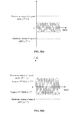
  • FIG. 5 further shows the relations of the first signed signal (I i ) 211 a and the second signed signal (Q i ) 211 b and their powers of the present invention.
  • the signed output that is, the first signed signal (I i ) 211 a and the second signed signal (Q i ) 211 b range is from ⁇ 2 N-1 to 2 N-1 ⁇ 1 including zero.
  • the fast and robust AGC apparatus 100 determines the extra gain only by checking the ADC saturation outputs, that is, the first signed signal (I i ) 211 a and the second signed signal (Q i ) 211 b , it is hard to settle the AGC gain in a few microseconds against a received WLAN signal whose dynamic range can be 90 dB (or more).
  • the ADC saturations provide insufficient information in the following cases: (1) when the signal is much bigger (lots of saturated/clipped ADC samples) or (2) when the signal is much smaller in power (far from ADC saturation).
  • a traditional AGC algorithm as shown in FIG. 2 , operates according to the AGC power error and slowly adjusts the AGC gain. This AGC process could therefore take significant time to converge for the above two cases.
  • a useful indication for proper gain setting of the fast and robust AGC apparatus 100 is to compare the power of the first signed signal (I i ) 211 a and the second signed signal (Q i ) 211 b , with the “saturations” of the 2 nd or the 3 rd MSB.
  • P MSB1 is about four times of P MSB2 , i.e., 6 dB higher in the power scale.
  • a series of reference power and amplitude levels (P MSBk , MSB pk , and MSB nk ) with 6 dB resolutions can be obtained as shown in FIG. 5 .
  • P MSB1 denotes the maximum power of a pair of the first signed signal (I i ) 211 a and the second signed signal (Q i ) 211 b , when both samples are equal to positive or negative maximum amplitude, can be one of the following three values: 2 ⁇ (2 N-1 ⁇ 1) 2 , (2 N-1 ⁇ 1) 2 +(2 N-1 ) 2 , or 2 ⁇ 2 2(N-1)
  • the first maximum power value occurs when both the first signed signal (I i ) 211 a and the second signed signal (Q i ) 211 b are 2 N-1 ⁇ 1
  • the second value occurs when one of the first signed signal (I i ) 211 a and the second signed signal (Q i ) 211 b is 2 N-1 ⁇ 1 and another is ⁇ 2 N-1
  • the third value occurs when both the first signed signal (I i ) 211 a and the second signed signal (Q i ) 211 b are ⁇ 2 N-1 .
  • N is typically no less than 8 and the differences can typically be ignored.
  • P msB1 2 ⁇ (2 N-1 ⁇ 1) 2 in all the discussions below.
  • P MSB2 2 ⁇ 2 (N-2) denotes roughly a 6 dB back off in power from P MSB1
  • P MSB3 2 ⁇ 2 (N-3) denotes roughly a 12 dB back off in power from P MSB1
  • MSB p1 denotes the “positive” saturation amplitude 2 N-1 ⁇ 1
  • MSB n1 denotes the “negative” saturation amplitude ⁇ 2 N-1 for the first signed signal (I i ) 211 a and the second signed signal (Q i ) 211 b .
  • MSB pk (k ⁇ 2) denotes the “positive” amplitude of the k-th MSB (Most Significant Bit) 2 N-k for the first signed signal (I i ) 211 a and the second signed signal (Q i ) 211 b
  • MSB nk denotes the “negative” amplitude of the k-th MSB ⁇ 2 N-k for the first signed signal (I i ) 211 a and the second signed signal (Q i ) 211 b
  • the equations and arrows in FIG. 5 are used to show the corresponding power of the first signed signal (I i ) 211 a and the second signed signal (Q i ) 211 b with the power levels: P MSB1 , P MSB2 , and P MSB3 .
  • any appropriate power resolution e.g. 1 dB or a fraction of it.
  • using the integer number of MSB power saturation/non-saturation is the simplest and intuitive implementation but one skills in the art can set new conditions of changing the gains which are not bounded by the integer bits of k-th MSB saturations/non-saturation, or k-th MSB power saturation/non-saturation as discussed above.
  • Step1 determining the amplitude statistics including the number of a plurality of ADC Most-Significant-Bit (MSB) saturations, the number of a plurality of ADC k-th Most-Significant-Bit (MSB) saturations and the number of ADC k-th Most-Significant-Bit (MSB) non-saturations within a plurality of M pairs of the first signed signal (I i ) 211 a and the second signed signal (Q i ) 211 b , Step2: determining an additional AGC gain adjustment ( ⁇ Aided ) 121 according to the amplitude statistics obtained in step1.
  • Step2 determining the amplitude statistics including the number of a plurality of ADC Most-Significant-Bit (MSB) saturations, the number of a plurality of ADC k-th Most-Significant-Bit (MSB) saturations and the number of ADC k-th Most-Significant-Bit (MSB)
  • the amplitude statistics further comprises cases of: Case1: if the amplitudes of the first signed signal (I i ) 211 a or the second signed signal (Q i ) 211 b is equal to 2 N-1 ⁇ 1 or ⁇ 2 N-1 , the number of a plurality of ADC Most-Significant-Bit (MSB) saturations is increased by one. Case2: if the absolute value of the first signed signal (I i ) or the second signed signal (Q i ) is greater than or equal to 2 N-k , the number of a plurality of ADC k-th Most-Significant-Bit (MSB) saturations is increased by one, where k is an integer from 2 to N.
  • Case1 if the amplitudes of the first signed signal (I i ) 211 a or the second signed signal (Q i ) b is equal to 2 N-1 ⁇ 1 or ⁇ 2 N-1 , the number of a plurality of ADC Most-Sign
  • Case3 if the absolute value of the first signed signal (I i ) or the second signed signal (Q i ) is smaller than 2 N-k , the number of ADC k-th Most-Significant-Bit (MSB) non-saturations is increased by one, where k is an integer from 2 to N.
  • MSB Most-Significant-Bit
  • the step2 further comprises cases of: Case1: if there are m Most-Significant-Bit (MSB) saturations out of the plurality of M pairs of the first signed signal (I i ) 211 a and the second signed signal (Q i ) 211 b , an additional AGC gain adjustment ( ⁇ Aided ) 121 is applied, where ⁇ Aided is a real number from 0 to ⁇ 30 dB, and m is an integer from 0 to M.
  • MSB Most-Significant-Bit
  • Case2 if there are m k-th Most-Significant-Bit (MSB) saturations out of a plurality of M pairs of the first signed signal (I i ) 211 a and the second signed signal (Q i ) 211 b , an additional AGC gain adjustment ( ⁇ Aided ) 121 is applied, where ⁇ Aided is a real number from ⁇ 40 to 40 dB, m is an integer from 0 to M, and k is an integer from 2 to N.
  • MSB Most-Significant-Bit
  • Case3 if there are consecutive j sets of the plurality of M pairs of the first signed signal (I i ) 211 a and the second signed signal (Q i ) 211 b with m k-the MSB non-saturations, an additional AGC gain adjustment ( ⁇ Aided ) is applied, wherein ⁇ Aided is a real number from ⁇ 40 to 40 dB, j is an integer from 1 to 5, m is an integer from 0 to M, and k is an integer from 2 to N.
  • ⁇ Aided is a real number from ⁇ 40 to 40 dB
  • j is an integer from 1 to 5
  • m is an integer from 0 to M
  • k is an integer from 2 to N.
  • Step1 determining the power statistics including the number of a plurality of ADC Most-Significant-Bit (MSB) power saturations, the number of a plurality of ADC k-th Most-Significant-Bit (MSB) power saturations and the number of ADC k-th Most-Significant-Bit (MSB) power non-saturations within a plurality of M pairs of the first signed signal (I i ) 211 a and the second signed signal (Q i ) 211 b .
  • Step2 determining an additional AGC gain adjustment ( ⁇ Aided ) 121 according to the power statistics obtained in Step1.
  • the power statistics further comprise cases of: Case1: if the sum of squares of any pair of the plurality of M pairs of the first signed signal (I i ) 211 a and the second signed signal (Q i ) 211 b is equal to or greater than 2 ⁇ (2 N-1 ⁇ 1), the number of a plurality of ADC Most-Significant-Bit (MSB) power saturations is increased by one.
  • Case1 if the sum of squares of any pair of the plurality of M pairs of the first signed signal (I i ) 211 a and the second signed signal (Q i ) 211 b is equal to or greater than 2 ⁇ (2 N-1 ⁇ 1), the number of a plurality of ADC Most-Significant-Bit (MSB) power saturations is increased by one.
  • Case2 if the sum of squares of any pair of the plurality of M pairs of the first signed signal (I i ) 211 a and the second signed signal (Q i ) 211 b is greater than or equal to 2 ⁇ 2 2(N-k) , the number of a plurality of ADC k-th Most-Significant-Bit (MSB) saturations power is increased by one, where k is an integer from 2 to N.
  • MSB Most-Significant-Bit
  • Case3 if the sum of squares of any pair of the plurality of M pairs of the first signed signal (I i ) 211 a and the second signed signal (Q i ) 211 b is smaller than 2 ⁇ 2 2(N-k) , the number of ADC k-th MSB power non-saturations is increased by one, where k is an integer from 2 to N.
  • the step2 further comprises cases of: Case1: if there are m Most-Significant-Bit (MSB) power saturations out of the plurality of M pairs of the first signed signal (I i ) 211 a and the second signed signal (Q i ) 211 b , an additional AGC gain adjustment ( ⁇ Aided ) 121 is applied, where ⁇ Aided is a real number from 0 to ⁇ 30 dB and m is an integer from 0 to M.
  • MSB Most-Significant-Bit
  • Case2 if there are m k-th Most-Significant-Bit (MSB) power saturations out of the plurality of M pairs of the first signed signal (I i ) 211 a and the second signed signal (Q i ) 211 b , an additional AGC gain adjustment ( ⁇ Aided ) 121 is applied, where ⁇ Aided is a real number from ⁇ 40 to 40 dB, m is an integer from 0 to M, and k is an integer from 2 to N.
  • MSB Most-Significant-Bit
  • Case3 if there are consecutive j sets of the plurality of M pairs of the first signed signal (I i ) 211 a and the second signed signal (Q i ) 211 b with m k-th MSB power non-saturations, an additional AGC gain adjustment ( ⁇ Aided ) is applied, wherein ⁇ Aided is a real number from ⁇ 40 to 40 dB, j is an integer from 1 to 5, m is an integer from 0 to M, and k is an integer from 2 to N.
  • ⁇ Aided is a real number from ⁇ 40 to 40 dB
  • j is an integer from 1 to 5
  • m is an integer from 0 to M
  • k is an integer from 2 to N.
  • FIG. 6 it shows the first embodiment of the relation of a signed, 3-bit ADC outputs and their powers of the present invention.
  • a few simple power and amplitude indicators for “signal power too high” can be defined as follows, also referring to conditions shown on the right-hand-side of FIG. 6 .
  • MSB_k ⁇ _sat ⁇ True , if ⁇ ( I i ⁇ MSB pk ⁇ ⁇ or ⁇ ⁇ I i ⁇ MSB nk ) ⁇ ⁇ or ( Q i ⁇ MSB pk ⁇ ⁇ or ⁇ ⁇ Q i ⁇ MSB nk ) ⁇ False , otherwise ; 2 ⁇ k ⁇ N Eq . ⁇ ( 3 )
  • FIG. 6 also shows a couple of simple amplitude indicators for “signal power too low”.
  • MSB_k ⁇ _null ⁇ True , if ⁇ ( I i ⁇ MSB pk ⁇ ⁇ and ⁇ ⁇ I i > MSB nk ) ⁇ ⁇ and ( Q i ⁇ MSB pk ⁇ ⁇ and ⁇ ⁇ Q i > MSB nk ) ⁇ False , otherwise ; 1 ⁇ k ⁇ N Eq . ⁇ ( 4 )
  • MSB_k_null defines a useful indication for the ADC gain being too small.
  • the desired signal power is set to be P msb — 2 (i.e., 6 dB back-off from the maximum power level) but all paired ADC outputs are in the region between MSB p4 and MSB n4 for a long observation time (consecutive samples) in statistics, the AGC gain is set too low for at least 12 dB.
  • FIG. 7 it shows a second embodiment of the amplitude and the power statistics of 8 pairs of ADC outputs according to the method of the present invention.
  • the first signed signal (I i ) 211 a and the second signed signal (Q i ) 211 b statistics based on simple indicators described in the above are used to check if AGC gain is grossly off.
  • FIG. 7 a few conditions (Conditions (I i )-(VI)) showing a clear AGC gain mismatch are given.
  • the corresponding “additional” AGC gain adjustments in dB are shown in the second column.
  • the third column contains the “reasons” why additional gain adjustments are recommended.
  • Condition (I i ) has 6 out of 8 (I i , Q i ) sample pairs with Most-Significant-Bit (MSB) power saturations.
  • ⁇ Aided ⁇ 15 dB in the second column.
  • ⁇ Aided ⁇ 15 dB in the second column.
  • ⁇ Aided a brief reason for the adjustment is given.
  • the additional AGC gain adjustment ( ⁇ Aided ) 121 can be accomplished by properly setting the value of ⁇ Aided for the adder 150 .
  • the last row of FIG. 7 shows all the dots (“ . . . ”) as more conditions and corresponding additional AGC gains can be added if so desired.
  • FIG. 8 shows a third embodiment of the amplitude and the power statistics of 16 pairs of ADC outputs according to the method of the present invention.
  • the first signed signal (I i ) 211 a and the second signed signal (Q i ) 211 b only statistics based on simple signal “amplitude” indicators described in the above are used to check if AGC gain is grossly off
  • this embodiment is slightly different from the second embodiment shown in FIG. 7 as simple indicator based on signal power P msb — k — sat is not used.
  • a few conditions Conditions (I i )-(V) showing a clear AGC gain mismatch are given.
  • FIG. 9 shows a functional block diagram for a wireless transceiver of the present invention. It provides a wireless communication receiver with a fast and robust automatic gain control (AGC) gain setting, comprising: an antenna 210 , an antenna switch 220 , a RF receiver 240 , a baseband demodulator 250 .
  • the antenna 210 is used for receiving and transmitting a RF signal 211 .
  • the antenna switch 220 is electrically connected to the antenna 210 . While transmitting, the antenna switch 220 position is such that the transmitter 230 is connected to the antenna 210 and the RF receiver 240 is normally turned off to save power.
  • AGC automatic gain control
  • the antenna switch 220 is positioned such that the RF receiver 240 is connected to the antenna 210 , and the transmitter 230 is normally turned off in order not to interfere with the receiver.
  • the RF receiver 240 is used for providing a first signal 2424 and a second signal 2434 according to the RF signal 211 and the LNA and VGA gain control signal 181 .
  • the baseband demodulator 250 electrically connected to the RF receiver 240 is used for providing a LNA and VGA gain control signal 181 to the RF receiver 240 and generating a demodulated signal 257 .
  • the RF receiver 240 further comprises: a plurality of stages of low noise amplifier (LNAs) 241 , a first plurality of variable gain amplifiers (VGAs) 2423 , a second plurality of variable gain amplifiers (VGAs) 2433 .
  • the plurality of stages of low noise amplifier (LNAs) 241 which is electrically connected to the antenna switch 220 , is used for amplifying the RF signal 211 .
  • the first plurality of variable gain amplifiers (VGAs) 2423 which is electrically connected to the plurality of stages of low noise amplifier (LNAs) 241 through a first filter 2422 and a first mixer 2421 , is used for providing a first signal 2424 .
  • the second plurality of variable gain amplifiers (VGAs) 2433 which is electrically connected to the plurality of stages of low noise amplifier (LNAs) 241 through a second filter 2432 and a second mixer 2431 , is used for providing a second signal 2434 .
  • VGAs variable gain amplifiers
  • the baseband demodulator 250 further comprises: a first N-bit analog-to-digital converter (ADCs) 251 , a second N-bit analog-to-digital converter (ADCs) 252 , a first analog-to-digital converter 253 , a second analog-to-digital converter 254 , a digital automatic gain control (AGC) module 100 , a baseband demodulator processor 256 .
  • the first N-bit analog-to-digital converter (ADCs) 251 electrically connected to the first plurality of variable gain amplifiers (VGAs) 2423 is used for converting the first signal 2424 output by the first plurality of variable gain amplifiers (VGAs) 2423 into an first unsigned signal 2511 .
  • the second N-bit analog-to-digital converter (ADCs) 252 electrically connected to the second plurality of variable gain amplifiers (VGAs) 2433 is used for converting the second signal 2434 output by the second plurality of variable gain amplifiers (VGAs) 2433 into an second unsigned signal 2521 .
  • the first analog-to-digital converter 253 electrically connected to the first N-bit analog-to-digital converter (ADCs) 251 is used for converting the first unsigned signal 2511 to a first signed signal (I i ) 2531 .
  • the second analog-to-digital converter 254 electrically connected to the second N-bit analog-to-digital converter (ADCs) 252 is used for converting the second unsigned signal 2521 to a second signed signal (Q i ) 2541 .
  • the fast and robust automatic gain control (AGC) module 100 which is electrically connected to the first analog-to-digital converters 253 and the second analog-to-digital converter 254 , is used for providing an automatic gain control (AGC) gain setting.
  • the baseband demodulator processor 256 which is electrically connected to the first analog-to-digital converter 253 and the second analog-to-digital converter 254 , is used for processing the first signed signal (I i ) 2531 and the second signed signal (Q i ) 2541 and providing a demodulated signal 257 .

Abstract

The present invention discloses apparatus and method for fast and robust automatic gain control (AGC). By using the power statistics and/or the amplitude statistics of multiple pairs of signed ADC outputs, the additional gain control can be determined and included in a statistics-aided AGC to successfully complete the AGC function for a received signal having a dynamic range up to 100 dB within a few micro-seconds.

Description

BACKGROUND OF THE INVENTION
1. Field of the Invention
The present invention relates to fast and robust apparatus used for wireless communication systems, such as but not limited to wireless local area networks (WLAN), and in particular to a fast and robust apparatus having an automatic gain control (AGC) gain setting.
2. Background
The present invention relates to wireless communication systems, such as but not limited to wireless local area networks (WLAN), and in particular to an 802.11a/b/g/n receiver base-band modem that provides a fast and robust automatic gain control (AGC) function for various RF transceiver ICs. In a typical WLAN environment, the received signal strength can vary with a dynamic range up to 100 dB depending on the distance between a transmitter and a receiver. An Automatic Gain Control (AGC) circuitry has been widely used in WLAN receivers to optimize its range performance.
While implemented, a typical WLAN transceiver consists of three chips, one power amplifier (PA) chip, one RF transceiver chip, and one integrated base-band (BB) and Medium Access Control (MAC) chip. To further lower down the total cost of a WLAN transceiver, integration of the PA chip into the RF transceiver chip has been achieved. Development effort in accomplishing a single-chip WLAN transceiver implementation has also been announced. FIG. 1 shows a functional block diagram for a wireless transceiver, which includes a direct-conversion (also known as zero-IF) receiver, for WLAN applications. At the highest level, it contains four functional blocks: an antenna 11, an antenna switch 12, a transmitter 20 and a receiver 10. While transmitting, the antenna switch position is such that a transmitter is connected to the antenna and the RF receiver is normally turned off to save power. While receiving, the antenna switch is positioned such that the RF receiver is connected to the antenna, and the transmitter is normally turned off. For all the discussions below, one can assume that the transceiver is in the receiving mode and the transmitter is turned off.
As is shown in FIG. 1, a typical zero-IF receiver 10 consists of a Low Noise Amplifier (LNA) 13, a pair of mixer 14 a and 14 b, a pair of channel selection filter 17 a and 17 b, and a pair of multiple stages of Variable Gain Amplifiers (VGA's) 18 a and 18 b. The LNA 13 is used to amplify a weak received signal with minimum distortion. In other words, the LNA Block 13 is used to enhance the sensitivity of the receiver. To provide the best sensitivity, a LNA stage provides a gain about 15 dB with a noise figure (NF) between 1.5 to 2.5 dB. Multiple stages of LNA's can be used to further enhance the receiver sensitivity in the presence of a weak received signal.
In the presence of a very strong signal, it is usually desirable to turn off some or all stages of the LNA's if multiple LNA's are used. The output of the LNA 13 is connected to a pair of mixers 14 a and 14 b. To keep the fidelity of the received signal, two mixers are required to provide an in-phase and a quadrature phase base-band signals. One mixer 14 a, which takes the carrier generated by the synthesizer 16 as one input and the LNA 13 output as another input, converts the received Radio Frequency (RF) signal to a base-band in-phase signal (also known as I-channel) as its output. While the other mixer 14 b, which uses a 90-degree phase-shifted carrier 15 as one input and the LNA 13 output as another input, to convert the received RF signal to a baseband quadrature-phase signal (also known as Q-channel) as its output. In what follows, the received in-phase and quadrature signals will be referred as I-channel and Q-channel signals, respectively. From now on, the processing of both I-channel and Q-channel signals is essentially the same. So it is sufficient to describe the processing of the I-channel signal.
For the I-channel signal, a low-pass Filter 17 a is applied to the corresponding mixer output to filter out the adjacent channel interferences and the unwanted mixer output at twice the RF signal frequency. The I-channel filter output is connected to the Variable Gain Amplifiers (VGA) 18 a for gain adjustment. In this diagram, each VGA 18 a contains two Variable Gain Amplifier stages 19 a and 19 b) with their gain controlled by the AGC control signals (as shown in FIG. 1) generated by AGC 22. A designer may use 3 or more VGA stages to implement the VGA function 18 a. As its name shows, each VGA stage 19 a or 19 b allows one to adjust its control voltage for providing variable gain to its input signal. The output of the VGA 18 a is connected to an analog-to-digital converter (ADC) 21 a of the base-band modem 40. The ADC 21 a digitizes and coverts an input signal to the signed ADC samples from 210 a to facilitate further processing of the received signal by the base-band demodulator processor 23 in digital domain. Detail operations will be presented later.
To fully utilize the dynamic range of an ADC, the input to an ADC needs to be maintained at or close to an optimal level. This is achieved by the AGC circuitry 22. The AGC circuitry, most commonly implemented in the base-band demodulator receiver 40, estimates the received signal strength and then properly adjusts the modes of the LNA 13 and the gains of the VGA's 18 a and 18 b in the RF receiver. The MUX 2220 is used to select a digital or analog AGC control signal according to its RF Receiver 30. If the AGC gain is controlled by an analog signal, a digital-to-analog converter (DAC) 2210 is required to convert the digital AGC control signal to the correspondent analog control signal.
For an 802.11a/b/g/n receiver to achieve optimal performance, this function needs to be accomplished in about 2 micro-seconds. This requirement makes the AGC function a challenge with a received signal strength variation of up to 100 dB.
More details on the AGC function will be presented below. To properly support the AGC function, one can use multiple stages of VGA's 18 a and 18 b. The total gain of the VGA's is usually controlled by the AGC 22 in the base-band demodulator 40. Dependent on its control voltage, a typical VGA stage can provide a gain from 0 dB to around 25 dB. With two to three stages of VGA's, a total received signal dynamic range around 75 dB can be supported. This is insufficient to support a dynamic range of up to 100 dB. Therefore, some RF transceivers provide either (1) means for switching off its low noise amplifier (LNA) and/or an intentional mis-matched antenna switch connection or (2) multiple switch-able stages of LNA's to extend the receive signal dynamic range further.
For IEEE 802.11g or 802.11n WLAN application, it is required to detect the signal presence and determine the signal strength (for AGC to settle close to its final gain), and turn on or off the LNA stages (or, equivalently in a two-stage LNA design, set the LNA gain to maximum by turning on both LNA stages, medium by turning off one LNA stage, or minimum by turning off both LNA stages) as necessary, all within about 2 micro-seconds. Hence, the implementation of the AGC circuitry becomes even more critical to an 802.11b, 802.11g, 802.11a, or 802.11n WLAN receiver.
For a detailed discussion, a traditional AGC 22 is shown in FIG. 2. Since the ADC digitizes the received analog waveform and provides unsigned integers as outputs, the paired ADC outputs from both channels are coupled into a pair of Converters 210 a and 201 b. The signed ADC output samples are obtained in 210 a and 210 b by subtracting the middle value of an N-bit ADC's dynamic range from the unsigned ADC output samples. After the paired Converters, the signed outputs of the i-th received samples (which are denoted as Ii and Qi) are coupled into the Power Detector 224. The measured power (Pi) of the i-th paired samples is then compared with the desired digitized signal power (PD). PD is typically chosen such that the full dynamic range of the ADC can be used. The multiplier 222 is used to control the AGC loop gain, which has an adjustable gain, k. The accumulator 228 uses an adder 228 a and a delay 228 b to track the history of accumulated AGC power error. The accumulator 228 output is an appropriate digital gain value, linear. Since VGA and LNA gains are typically adjusted in dB while the digital value Giinear is evaluated in “linear” domain, a VGA/LNA gain mapping 223 typically takes the digital value linear and converts into to proper LNA and VGA gain control signals.
One may measure and average more pair of I/Q samples before the subtractor 226 for a better power measurement in statistics. However, the more samples are measured, the slower the AGC gain is adjusted. The other drawback of this AGC operation is from the saturated samples. In order to be able to receive the smallest signal, the AGC 22 is initially set to have the maximum gain when no signal was present (noise only). For a better explanation, a few I or Q waveforms, when the ADC is allowed to have unlimited number of bits, after the Converters 210 a and 210 b are shown in FIG. 3. Two dashed horizontal lines show the levels at which the waveform samples would have been clipped for an N-bit ADC. When a waveform sample was clipped, an N-bit ADC was called “saturated” below. For a pair of N-bit ADCs, the dynamic signal range (in dB) is proportional to the bit-number, N. However, the greater N is, the higher cost is to build this pair of ADCs. For a practical WLAN system, the bit number N used is much smaller than its signal dynamic range (around 100 dB). Therefore, the dynamic range of an incoming signal (depending upon the distance between a transmitter and the receiver) may be 30 dB or greater in power than that of a pair of N-bit ADCs. With the AGC gain set at maximum while waiting for a WLAN signal, the presence of a WLAN signal will typically cause most or all N-bit ADC outputs being saturated, as shown in FIG. 3 a and FIG. 3 b. For explanation simplicity, it is assumed that the number of ADC output saturations in Cases A and B is similar. Since a pair of saturated ADC output does not provide the information as to how big the input signal power is compared to the maximal ADC dynamic range, the estimated AGC power errors are insufficient for the AGC block to determine the correct AGC gain, which should be a few dB lower in Case A, and quite a few dB lower in Case B. A greater reduction in AGC gain is desirable for Case B, while the same gain reduction would have caused the received signal to be too small at the output of the ADC for Case A.
When AGC sometimes over-reacts, it can cause the digitized samples to be much smaller such as shown in FIG. 3 c and FIG. 3 d. The conventional AGC algorithm applied for these cases can be explained as follows. For a faster convergence, a higher loop gain 222 can cause AGC gain oscillation and the AGC loop may become unstable. On the other hand, a smaller loop gain 222 will take a significant time for the AGC block to converge to the desired AGC gain. Intuitively, one may count the statistics of the saturation of ADC outputs to aid the AGC block. In cases of FIG. 3 c and FIG. 3 d, if one counts not only the saturations of the ADC outputs but also the “saturations” of several other power levels as shown in FIG. 3 c and FIG. 3 d, a better estimate of received signal power can be obtained.
A traditional AGC loop (without saturation-detection aided algorithm) as shown in FIG. 2 requires significant time for AGC gain to converge and hence is not suitable for applications like WLAN. Typically, the loop gain is set to be small for a slow but smooth AGC gain convergence. The power error of ADC output samples are averaged for a sufficient time for a better power estimate in statistics. When a higher AGC gain is used for a fast converge AGC loop, the AGC gain may be oscillating too much and the system performance is degraded. A slow convergence AGC loop is not suitable for a system requires AGC gain to converge within a few micro-seconds, e.g., a WLAN packet with very short preambles (or short training sequence). The aided algorithm should be used to shorten the AGC convergence time.
A traditional saturation-detection aided AGC algorithm uses the saturated ADC samples only, i.e., 0 and 2N−1 for an N-bit ADC. However, a 802.11a/g/n WLAN signal uses OFDM modulation which can have a peak-to-average power ratio around 10 dB. For such a modulated signal, a back-off of more than 6 dB is typically required so the signal is not clipped (distorted) going through the ADC. In this case, the ADC saturation in statistics is a rare event and it is not a useful indication to determine if the AGC gain is too high or not. In addition, the ADC saturation indicates the AGC gain may be too high but there is no aided algorithm for the cases when the AGC gain is too low. Therefore, it is faster and easier to adjust the AGC from high gain to low gain than to adjust the AGC from low gain to high gain for a traditional saturation-detection aided algorithm. Furthermore, a traditional Receive Signal Strength Indicator (RSSI) aided AGC algorithm requires significant time for an accurate RSSI estimate; a drawback for a WLAN system which requires a quick and fast AGC convergence. In addition, a long RSSI measurement time results in a slow AGC gain adjustment, and hence less time remains for a traditional AGC loop (FIG. 2) which is slow but precise in gain convergence, a desirable property for AGC gain fine-tuning Furthermore, since a lock-up time (with fixed AGC gain) is required for an accurate RSSI measurement, this lock-up time can cause the loss of a WLAN packet with a very short preamble or training sequence, in case the receiver gets into a false alarm mode immediately before the arrival the packet.
This invention application is focused on the AGC 22 which is part of the receiver function. The overall amplifier gain provided by a receiver (including LNAs and VGAs) is denoted as “AGC gain” in this application. In general, the higher the received signal power, the smaller the AGC gain is provided by the receiver. The AGC 22 is used to measure the received signal power and apply an appropriate AGC gain (by changing LNA on/off states and/or VGA gains) so the received signal is appropriately amplified and the outputs of VGAs 18 can fully utilize the designed dynamic range of an ADC. If the AGC gain is too high, the ADC will be saturated and the ADC output signal is distorted. If the AGC gain is too small, the ADC outputs are too small (a waste of the ADC's dynamic range), which can cause the baseband demodulator processor to decode the data incorrectly. In summary, the system performance will be degraded in both cases. In practice, the AGC function needs to correctly estimate the received signal power of a wideband 802.11a/b/g/n signal within a few micro-seconds by adjusting the VGA gains and, if needed, switching off one or more LNA stages which has a settling time of a couple hundreds of nano-seconds each to achieve a receiver dynamic range around 100 dB. To implement a fast-and-precise AGC algorithm in a few micro-seconds for a receive signal with a 100 dB dynamic range is a great challenge for any WLAN receiver. Therefore, the purpose of this invention application is to provide a few simple-fast-and-reliable aided AGC algorithms for AGC 22 during coarse and fine AGC tunings.
This invention presents an innovative statistics-aided AGC algorithm based on the statistics of the ADC outputs. The benefit of using this digital AGC algorithm is multifold: (1) it provides a simple aided algorithm to be appended to a traditional AGC block 22, (2) it provides a faster and more robust AGC convergence than a tradition aided AGC algorithm, and (3) it provides a generic algorithm that can be applied to the front-end of various RF receivers, which typically are required to detect a signal with up to 100 dB power variations.
U.S. Pat. No. 7,936,850, issued to Eric Rodal et al. entitled “Method and apparatus for providing a digital automatic gain control (AGC)” discloses a logarithmic analog-to-digital converter for sampling the analog RF signals, a FIR filter for filtering the digitized signals, a re-sampler for re-sampling the digitized signals, and an automatic gain control circuit. This patent application is focused on an automatic gain control function which controls the resampling of the first plurality of bits to form the second plurality of bits in accordance with an automatic gain control signal.
According above discussions, it need a method and apparatus to overcome the disadvantage of the prior art.
BRIEF SUMMARY OF THE INVENTION
It is an objective of the present invention to provide a fast and robust AGC apparatus. By using the power statistic or the amplitude statistic of the pairs of N-bit I and Q channel unsigned ADC outputs, an additional AGC gain can be determined to ensure a fast and robust AGC implementation which provides the LNA on/off and the VGA gain control signal.
It is another objective of the present invention to provide an automatic gain control (AGC) method using amplitude statistics of I and Q channel samples.
It is another objective of the present invention to provide an automatic gain control (AGC) method using power statistics of I and Q channel samples.
It is another objective of the present invention to provide a wireless communication transceiver with an automatic gain control (AGC).
To achieve the above objective, the present invention provides a fast and robust automatic gain control (AGC) apparatus with an additional AGC gain adjustment (ΔAided) comprising: a power detector, a statistics-aided AGC algorithm unit, a subtractor, an average unit, an adder, a multiplier, an accumulator, and a LNA AND VGA control mapping unit. The first signed signal (Ii) is provided by a first analog-to-digital converter. The second signed signal (Qi) is provided by a second analog-to-digital converter. The power detector, electrically connected to the first analog-to-digital converter and the second analog-to-digital converter, is used for providing a plurality of measured power (Pi), where Pi is equal to the sum of squares of the first signed signal (Ii) and the second signed signal (Qi).
The statistics-aided AGC algorithm unit, electrically connected to the first analog-to-digital converter, the second analog-to-digital converter and the power detector, is used for determining an additional AGC gain adjustment (ΔAided) according to the amplitude statistics of the plurality of M pairs of the first signed signal (Ii) and the second signed signal (Qi), and/or the power statistics of the corresponding plurality of measured power (Pi), wherein M is an integer from 1 to 100;
The subtractor, electrically connected to the power detector, is used for evaluating a power differences between a desired received signal power (PD) and each of the plurality of measured power (Pi) and providing a plurality of AGC power error signals. The average unit, electrically connected to the subtractor, is used for averaging the plurality of AGC power error signals and providing an average AGC power error signal. The adder, electrically connected to the average unit and the statistics-aided AGC algorithm unit, is used for providing a gain adjustment by adding the additional AGC gain adjustment (ΔAided) to the average AGC power error signal. The multiplier, electrically connected to the adder, is used for controlling a AGC loop gain by an adjustable gain (k). The accumulator, electrically connected to the multiplier, is used for tracking the history of accumulations of the average AGC power error signal and providing an appropriate digital gain value (Glinear). The LNA AND VGA control mapping unit electrically connected to the accumulator is used for converting the appropriate digital gain value (Glinear) into a LNA AND VGA gain control signal.
To achieve another objective, the present invention provides an automatic gain control (AGC) method using amplitude statistics, comprising steps of: Step1: determining the amplitude statistics including the number of a plurality of ADC Most-Significant-Bit (MSB) saturations, the number of a plurality of ADC k-th Most-Significant-Bit (MSB) saturations and the number of ADC k-th Most-Significant-Bit (MSB) non-saturations within a plurality of M pairs of the first signed signal (Ii) and the second signed signal (Qi), Step2: determining an additional AGC gain adjustment (ΔAided) according to the amplitude statistics obtained in Step1.
According to one aspect of the present invention, the amplitude statistics further comprises cases of: case1: if one or both of the amplitudes of the first signed signal (Ii) and the second signed signal (Qi) is equal to 2N-1−1 or −2N-1, the number of a plurality of ADC Most-Significant-Bit (MSB) saturations is increased by one, case2: if one or both absolute values of any pair of the amplitudes of the first signed signal (Ii) and the second signed signal (Qi) are greater than or equal to 2N-k, the number of a plurality of ADC k-th Most-Significant-Bit (MSB) saturations is increased by one where k is an integer from 2 to N, and case3: if both absolute values of any pair of the amplitudes of the first signed signal (Ii) and the second signed signal (Qi) are smaller than 2N-k, the number of ADC k-th Most-Significant-Bit (MSB) non-saturations within a total of M pairs of ADC outputs is increased by one where k is an integer from 2 to N.
According to one aspect of the present invention, the step2 further comprises cases of: case1: if there are m Most-Significant-Bit (MSB) saturations out of the plurality of M pairs of the first signed signal (Ii) and the second signed signal (Qi), an additional AGC gain adjustment (ΔAided) from 0 to −30 dB and m is an integer from 0 to M, case2: if there are m k-th Most-Significant-Bit (MSB) saturations out of the plurality of M pairs of the first signed signal (Ii) and the second signed signal (Qi), an additional AGC gain adjustment (ΔAided) can be a real number from −40 to 40 dB, where m is an integer from 0 to M, and k is an integer from 2 to N, and case3: if there are consecutive j sets of the plurality of M pairs of the first signed signal (Ii) and the second signed signal (Qi) with m k-th MSB non-saturations, an additional AGC gain adjustment (ΔAided) is applied, where ΔAided is a real number from −40 to 40 dB, j is an integer from 1 to 5, m is an integer from 0 to M, and k is an integer from 2 to N.
To achieve another objective, the present invention provides an automatic gain control (AGC) method using power statistics, comprising steps of: Step1: determining the power statistics including the number of a plurality of ADC Most-Significant-Bit (MSB) power saturations, the number of a plurality of ADC k-th Most-Significant-Bit (MSB) power saturations and the number of ADC k-th Most-Significant-Bit (MSB) power non-saturations within a plurality of M pairs of the first signed signal (Ii) and the second signed signal (Qi), Step2: determining an additional AGC gain adjustment (ΔAided) according to the power statistics obtained in Step1.
According to one aspect of the present invention, the power statistic further comprises cases of: case1: if the sum of squares of any pair of the plurality of M pairs of the first signed signal (Ii) and the second signed signal (Qi) is equal to or greater than 2×(2N-1−1), the number of a plurality of ADC Most-Significant-Bit (MSB) power saturations is increased by one, case2: if the sum of squares of any pair of the plurality of M pairs of the first signed signal (Ii) and the second signed signal (Qi) is greater than or equal to 2×22(N-k), the number of a plurality of ADC k-th Most-Significant-Bit (MSB) power saturations is increased by one where k is an integer from 2 to N, and case3: if the sum of squares of any pair of the plurality of M pairs of the first signed signal (Ii) and the second signed signal (Qi) is smaller than 2×22(N-k), the number of ADC k-th MSB power non-saturations is increased by one where k is an integer from 2 to N.
According to one aspect of the present invention, the step2 further comprises cases of: case1: if there are m Most-Significant-Bit (MSB) power saturations out of the plurality of M pairs of the first signed signal (Ii) and the second signed signal (Qi), an additional AGC gain adjustment (ΔAided) can be a real number from 0 to −30 dB, where m is an integer from 0 to M, case2: if there are m k-th Most-Significant-Bit (MSB) power saturations out of the plurality of M pairs of the first signed signal (Ii) and the second signed signal (Qi), an additional AGC gain adjustment (ΔAided) can be a real number from −40 to 40 dB, where m is an integer from 0 to M, and k is an integer from 2 to N, and case3: if there are consecutive j sets of the plurality of M pairs of the first signed signal (Ii) and the second signed signal (Qi) with m k-th MSB power non-saturations, an additional AGC gain adjustment (ΔAided) is applied, wherein ΔAided is a real number from −40 to 40 dB, j is an integer from 1 to 5, m is an integer from 0 to M, and k is an integer from 2 to N.
To achieve another objective, the present invention provides a wireless communication transceiver with an automatic gain control (AGC) for its receiving mode comprising: an antenna, an antenna switch, a RF receiver, a baseband demodulator. While in receiving mode, the antenna is used for receiving a RF signal. Although a transceiver typically has a transmitter, the antenna switch is positioned such that the RF receiver is connected to the antenna while the transceiver is in receiving mode, and the transmitter is normally turned off. While receiving, the RF receiver electrically connected to the antenna switch is used for providing a first signal and a second signal according to the RF signal. The baseband demodulator electrically connected to the RF receiver is used for providing a LNA and VGA gain control signal to the RF receiver and a demodulated signal.
According to one aspect of the present invention, the RF receiver further comprises: a plurality of stages of low noise amplifier (LNAs), a first plurality of variable gain amplifiers (VGAs), a second plurality of variable gain amplifiers (VGAs). The plurality of stages of low noise amplifier (LNAs) electrically connected to the antenna switch is used for amplifying the RF signal. The first plurality of variable gain amplifiers (VGAs) electrically connected to the plurality of stages of low noise amplifier (LNAs) through a first filter and a first mixer is used for amplifying a first signal output by the first filter and providing a first signal. The second plurality of variable gain amplifiers (VGAs) electrically connected to the plurality of stages of low noise amplifier (LNAs) through a second filter and a second mixer is used for amplifying a second signal output by the second filter and providing a second signal.
According to one aspect of the present invention, the baseband demodulator further comprises: a first N-bit analog-to-digital converter (ADCs), a second N-bit analog-to-digital converter (ADCs), a first analog-to-digital converter, a second analog-to-digital converter, a digital automatic gain control (AGC) module, a baseband demodulator processor. The first N-bit analog-to-digital converter (ADCs) electrically connected to the first plurality of variable gain amplifiers (VGAs) is used for converting the first signal output of the first plurality of variable gain amplifiers (VGAs) into an first unsigned signal. The second N-bit analog-to-digital converter (ADCs) electrically connected to the second plurality of variable gain amplifiers (VGAs) is used for converting the second signal output of the second plurality of variable gain amplifiers (VGAs) into a second unsigned signal. The first analog-to-digital converter electrically connected to the first N-bit analog-to-digital converter (ADCs) is used for converting the first unsigned signal to a first signed signal (Ii). The second analog-to-digital converter electrically connected to the second N-bit analog-to-digital converter (ADCs) is used for converting the second unsigned signal to a second signed signal (Qi). The digital automatic gain control (AGC) module electrically connected to the first analog-to-digital converters and the second analog-to-digital converter is used for providing an automatic gain control (AGC) gain setting. The baseband demodulator processor electrically connected to the first analog-to-digital converter and the second analog-to-digital converter is used for processing the first signed signal (Ii) and the second signed signal (Qi) and providing a demodulated signal, wherein the digital automatic gain control (AGC) module is the same as the apparatus in claim 1.
These and many other advantages and features of the present invention will be readily apparent to those skilled in the art from the following drawings and detailed descriptions.
BRIEF DESCRIPTION OF THE DRAWINGS
All the objects, advantages, and novel features of the invention will become more apparent from the following detailed descriptions when taken in conjunction with the accompanying drawings.
FIG. 1 shows a functional block diagram of a wireless transceiver including a direct down-conversion receiver of the prior art;
FIG. 2 shows a functional block diagram of a conventional AGC block of the prior art;
FIG. 3 shows the four cases of signal waveforms relative to their ADC full dynamic ranges of the prior art;
FIG. 4 shows a functional block diagram of the fast and robust automatic gain control (AGC) apparatus of the present invention;
FIG. 5 shows a relation of the first signed signal (Ii) and the second signed signal (Qi) and their powers of the present invention;
FIG. 6 shows a first embodiment of the relation of a signed, 3-bit ADC outputs and their powers of the present invention;
FIG. 7 shows a second embodiment of the amplitude and the power statistics of 8 pairs of ADC outputs according to the method of the present invention;
FIG. 8 shows a third embodiment of the amplitude and the power statistics of 16 pairs of ADC outputs according to the method of the present invention; and
FIG. 9 shows a functional block diagram for a wireless transceiver with an automatic gain control (AGC) of the present invention.
DETAILED DESCRIPTION OF THE INVENTION
Although the invention has been explained in relation to several preferred embodiments, the accompanying drawings and the following detailed descriptions are the preferred embodiment of the present invention. It is to be understood that the following disclosed descriptions will be examples of present invention, and will not limit the present invention into the drawings and the special embodiment.
To understand the spirit of the present invention, FIG. 4 shows a functional block diagram of the fast and robust automatic gain control (AGC) apparatus 100 with an additional AGC gain adjustment (ΔAided) of the present invention, wherein the fast and robust AGC apparatus 100 comprises: a power detector 110, a statistics-aided AGC algorithm unit 120, a subtractor 130, an average unit 140, an adder 150, a multiplier 160, an accumulator 170, a LNA and VGA control mapping unit 180. The first signed signals (Ii) 211 a and the second signed signals (Qi) 211 b are the two inputs to this AGC. The first signed signal (Ii) 211 a is provided by a first analog-to-digital converter 253. The second signed signal (Qi) 211 b is provided by a second analog-to-digital converter 254. The power detector 110, which is electrically connected to the first analog-to-digital converter 253 and the second analog-to-digital converter 254, is used for providing a plurality of measured power (Pi) 111, where Pi is equal to the sum of squares of the corresponding first signed signal (Ii) 211 a and second signed signal (Qi) 211 b. The statistics-aided AGC algorithm unit 120, which is electrically connected to the first analog-to-digital converter 253, the second analog-to-digital converter 254 and the power detector 110, is used for determining an additional AGC gain adjustment (ΔAided) 121 according to the amplitude statistics of the plurality of M pairs of the first signed signal (Ii) 211 a and the second signed signal (Qi) 211 b, and/or the power statistics of the corresponding measured power (Pi) 111, where M is an integer from 1 to 100. The subtractor 130, which is electrically connected to the power detector 110, is used for evaluating a power differences between a desired received signal power (PD) 112 and each of the plurality of measured power (Pi) 111 and providing a plurality of AGC power error signals 131, wherein the plurality of AGC power error signals 131 are equal to the desired received signal power (PD) 112 minus the plurality of measured power (Pi) 111. The average unit 140 electrically connected to the subtractor 130 is used for averaging the same M consecutive AGC power error signals 131 and providing an average AGC power error signal 141. To summarize, for each of the plurality of M pairs of the first signed signal (Ii) 211 a and the second signed signal (Qi) 211 b, an additional AGC gain adjustment (ΔAided) 121 is generated and is fed to the adder 150, which has the average AGC power error signal 141 as its second input. The adder 150, which is electrically connected to the average unit 140 and the statistics aided AGC algorithm unit 120, generates a corresponding gain adjustment 151 by adding the additional AGC gain adjustment (ΔAided) 121 to the average AGC power error signal 141. The multiplier 160, which is electrically connected to the adder 150, is used for controlling the AGC loop gain by multiplying the gain adjustment 151 by an adjustable gain (k). The accumulator 170, consisting of an adder 171 and a delay 172, is electrically connected to the multiplier 150. The accumulator 170 takes the gain adjusted plurality of average AGC power error signals 141, adds the gain adjusted plurality of average AGC power error signals 141 up, stores the results and outputs this accumulated value as an appropriate digital gain value (Glinear) 173. The LNA and VGA control mapping unit 180 electrically connected to the accumulator 170 is used for converting the appropriate digital gain value (Glinear) 173 into a LNA and VGA gain control signal 181.
The accumulator 170 further comprises: an adder 171 and a delay 172. The adder 171 is electrically connected to the multiplier 160. The delay 172 has an input terminal electrically connected to the adder and an output terminal electrically connected to the adder and the LNA and VGA control mapping unit.
Based on FIG. 4, FIG. 5 further shows the relations of the first signed signal (Ii) 211 a and the second signed signal (Qi) 211 b and their powers of the present invention. For an N-bit ADC, the signed output, that is, the first signed signal (Ii) 211 a and the second signed signal (Qi) 211 b range is from −2N-1 to 2N-1−1 including zero. Saturation occurs if the first signed signal (Ii) 211 a or the second signed signal (Qi) 211 b is equal to −2N-1 or 2N-1−1 indicating that gain of the fast and robust AGC apparatus 100 is too high and therefore the input signals of N-bit ADCs exceed the maximum ADC dynamic range. In this case, the output signals of N-bit ADCs, which are the inputs to the baseband demodulator processor, will be clipped (distorted) and the system performance is degraded. During the packet acquisition process, while the receiver is trying to detect the presence of a packet and to set gain of the fast and robust apparatus 100 properly, the initial AGC gain is typically set close to its maximum value in the absence of a signal. If the received signal power is 10 dB or more higher than the noise power, saturations are very likely to occur immediately upon the arrival of a packet. However, this is also a useful indication for the fast and robust AGC apparatus 100 to adjust the LNA or VGA gain setting if too many amplitude or power saturations occur in a short observation period from the theory of statistics.
However, if the fast and robust AGC apparatus 100 determines the extra gain only by checking the ADC saturation outputs, that is, the first signed signal (Ii) 211 a and the second signed signal (Qi) 211 b, it is hard to settle the AGC gain in a few microseconds against a received WLAN signal whose dynamic range can be 90 dB (or more). This is because the ADC saturations provide insufficient information in the following cases: (1) when the signal is much bigger (lots of saturated/clipped ADC samples) or (2) when the signal is much smaller in power (far from ADC saturation). In both cases, a traditional AGC algorithm as shown in FIG. 2, operates according to the AGC power error and slowly adjusts the AGC gain. This AGC process could therefore take significant time to converge for the above two cases.
Referring to FIG. 5 again, a useful indication for proper gain setting of the fast and robust AGC apparatus 100 is to compare the power of the first signed signal (Ii) 211 a and the second signed signal (Qi) 211 b, with the “saturations” of the 2nd or the 3rd MSB. For example, if both samples of a paired ADC I/Q outputs, the first signed signal (Ii) 211 a and the second signed signal (Qi) 211 b, are saturated, the calculated signal power becomes PMSB1=2·(2N-1−1)2, (2N-1−1)2+(2N-1)2), or 2·22(N-1), which is approximately equal to 2·(2(N-1)-1)2 for N no smaller than 8. Similarly, if the first signed signal (Ii) 211 a and the second signed signal (Qi) 211 b are one-halves of the ADC dynamic range, the calculated signal power Pi becomes PMSB2(=2·22(N-2)). One may found that the PMSB1 is about four times of PMSB2, i.e., 6 dB higher in the power scale. Similarly, a series of reference power and amplitude levels (PMSBk, MSBpk, and MSBnk) with 6 dB resolutions can be obtained as shown in FIG. 5. Specifically, for an N-bit ADC, PMSB1 denotes the maximum power of a pair of the first signed signal (Ii) 211 a and the second signed signal (Qi) 211 b, when both samples are equal to positive or negative maximum amplitude, can be one of the following three values: 2·(2N-1−1)2, (2N-1−1)2+(2N-1)2, or 2·22(N-1)
In the above, the first maximum power value occurs when both the first signed signal (Ii) 211 a and the second signed signal (Qi) 211 b are 2N-1−1, the second value occurs when one of the first signed signal (Ii) 211 a and the second signed signal (Qi) 211 b is 2N-1−1 and another is −2 N-1, and the third value occurs when both the first signed signal (Ii) 211 a and the second signed signal (Qi) 211 b are −2N-1. For WLAN implementations, N is typically no less than 8 and the differences can typically be ignored. Therefore, we will use PmsB1=2·(2N-1−1)2 in all the discussions below. Similarly, PMSB2=2·2(N-2) denotes roughly a 6 dB back off in power from PMSB1, and PMSB3=2□2(N-3) denotes roughly a 12 dB back off in power from PMSB1
As shown in FIG. 5, for an N-bit ADC, MSBp1 denotes the “positive” saturation amplitude 2N-1−1, and MSBn1 denotes the “negative” saturation amplitude −2N-1 for the first signed signal (Ii) 211 a and the second signed signal (Qi) 211 b. Similarly, MSBpk (k≧2) denotes the “positive” amplitude of the k-th MSB (Most Significant Bit) 2 N-k for the first signed signal (Ii) 211 a and the second signed signal (Qi) 211 b, and MSBnk denotes the “negative” amplitude of the k-th MSB −2N-k for the first signed signal (Ii) 211 a and the second signed signal (Qi) 211 b. The equations and arrows in FIG. 5 are used to show the corresponding power of the first signed signal (Ii) 211 a and the second signed signal (Qi) 211 b with the power levels: PMSB1, PMSB2, and PMSB3.
One may select any appropriate power resolution according to the specific application, e.g., 1 dB or a fraction of it. In other words, using the integer number of MSB power saturation/non-saturation is the simplest and intuitive implementation but one skills in the art can set new conditions of changing the gains which are not bounded by the integer bits of k-th MSB saturations/non-saturation, or k-th MSB power saturation/non-saturation as discussed above. For example, a PMSBk.25=22(N-k-0.25) power saturation/non-saturation is a value in the middle of the k-th and (k+1)th MSB power saturations.
To further understand the operating method of the fast and robust AGC apparatus 100, a method using the amplitude statistics is provided, comprising the steps of: Step1: determining the amplitude statistics including the number of a plurality of ADC Most-Significant-Bit (MSB) saturations, the number of a plurality of ADC k-th Most-Significant-Bit (MSB) saturations and the number of ADC k-th Most-Significant-Bit (MSB) non-saturations within a plurality of M pairs of the first signed signal (Ii) 211 a and the second signed signal (Qi) 211 b, Step2: determining an additional AGC gain adjustment (ΔAided) 121 according to the amplitude statistics obtained in step1.
The amplitude statistics further comprises cases of: Case1: if the amplitudes of the first signed signal (Ii) 211 a or the second signed signal (Qi) 211 b is equal to 2N-1−1 or −2N-1, the number of a plurality of ADC Most-Significant-Bit (MSB) saturations is increased by one. Case2: if the absolute value of the first signed signal (Ii) or the second signed signal (Qi) is greater than or equal to 2N-k, the number of a plurality of ADC k-th Most-Significant-Bit (MSB) saturations is increased by one, where k is an integer from 2 to N. Case3: if the absolute value of the first signed signal (Ii) or the second signed signal (Qi) is smaller than 2N-k, the number of ADC k-th Most-Significant-Bit (MSB) non-saturations is increased by one, where k is an integer from 2 to N.
Moreover, it also noted that the step2 further comprises cases of: Case1: if there are m Most-Significant-Bit (MSB) saturations out of the plurality of M pairs of the first signed signal (Ii) 211 a and the second signed signal (Qi) 211 b, an additional AGC gain adjustment (ΔAided) 121 is applied, where ΔAided is a real number from 0 to −30 dB, and m is an integer from 0 to M. Case2: if there are m k-th Most-Significant-Bit (MSB) saturations out of a plurality of M pairs of the first signed signal (Ii) 211 a and the second signed signal (Qi) 211 b, an additional AGC gain adjustment (ΔAided) 121 is applied, where ΔAided is a real number from −40 to 40 dB, m is an integer from 0 to M, and k is an integer from 2 to N. Case3: if there are consecutive j sets of the plurality of M pairs of the first signed signal (Ii) 211 a and the second signed signal (Qi) 211 b with m k-the MSB non-saturations, an additional AGC gain adjustment (ΔAided) is applied, wherein ΔAided is a real number from −40 to 40 dB, j is an integer from 1 to 5, m is an integer from 0 to M, and k is an integer from 2 to N.
To further understand the operating method of the fast and robust AGC apparatus 100, a method using the power statistics is provided, comprising steps of: Step1: determining the power statistics including the number of a plurality of ADC Most-Significant-Bit (MSB) power saturations, the number of a plurality of ADC k-th Most-Significant-Bit (MSB) power saturations and the number of ADC k-th Most-Significant-Bit (MSB) power non-saturations within a plurality of M pairs of the first signed signal (Ii) 211 a and the second signed signal (Qi) 211 b. Step2: determining an additional AGC gain adjustment (ΔAided) 121 according to the power statistics obtained in Step1.
The power statistics further comprise cases of: Case1: if the sum of squares of any pair of the plurality of M pairs of the first signed signal (Ii) 211 a and the second signed signal (Qi) 211 b is equal to or greater than 2×(2N-1−1), the number of a plurality of ADC Most-Significant-Bit (MSB) power saturations is increased by one. Case2: if the sum of squares of any pair of the plurality of M pairs of the first signed signal (Ii) 211 a and the second signed signal (Qi) 211 b is greater than or equal to 2×22(N-k), the number of a plurality of ADC k-th Most-Significant-Bit (MSB) saturations power is increased by one, where k is an integer from 2 to N. Case3: if the sum of squares of any pair of the plurality of M pairs of the first signed signal (Ii) 211 a and the second signed signal (Qi) 211 b is smaller than 2×22(N-k), the number of ADC k-th MSB power non-saturations is increased by one, where k is an integer from 2 to N.
Moreover, it is also noted that the step2 further comprises cases of: Case1: if there are m Most-Significant-Bit (MSB) power saturations out of the plurality of M pairs of the first signed signal (Ii) 211 a and the second signed signal (Qi) 211 b, an additional AGC gain adjustment (ΔAided) 121 is applied, where ΔAided is a real number from 0 to −30 dB and m is an integer from 0 to M. Case2: if there are m k-th Most-Significant-Bit (MSB) power saturations out of the plurality of M pairs of the first signed signal (Ii) 211 a and the second signed signal (Qi) 211 b, an additional AGC gain adjustment (ΔAided) 121 is applied, where ΔAided is a real number from −40 to 40 dB, m is an integer from 0 to M, and k is an integer from 2 to N. Case3: if there are consecutive j sets of the plurality of M pairs of the first signed signal (Ii) 211 a and the second signed signal (Qi) 211 b with m k-th MSB power non-saturations, an additional AGC gain adjustment (ΔAided) is applied, wherein ΔAided is a real number from −40 to 40 dB, j is an integer from 1 to 5, m is an integer from 0 to M, and k is an integer from 2 to N.
<Embodiment 1>
Referring to FIG. 6, it shows the first embodiment of the relation of a signed, 3-bit ADC outputs and their powers of the present invention. In brief summary, for each pair of the first signed signal (Ii) 211 a and the second signed signal (Qi) 211 b, a few simple power and amplitude indicators for “signal power too high” can be defined as follows, also referring to conditions shown on the right-hand-side of FIG. 6.
    • (a) Power Indicators:
P msb _ k _ sat = { True , if P i P msb_k False , otherwise for 1 k N Eq . ( 1 )
    • (b) Amplitude Indicators:
MSB_ 1 _sat = { True , if ( I i = MSB p 1 or I i = MSB n 1 ) or ( Q i = MSB p 1 or Q i = MSB n 1 ) False , otherwise Eq . ( 2 ) MSB_k _sat = { True , if ( I i MSB pk or I i MSB nk ) or ( Q i MSB pk or Q i MSB nk ) False , otherwise ; 2 k N Eq . ( 3 )
Similarly, FIG. 6 also shows a couple of simple amplitude indicators for “signal power too low”.
MSB_k _null = { True , if ( I i < MSB pk and I i > MSB nk ) and ( Q i < MSB pk and Q i > MSB nk ) False , otherwise ; 1 k N Eq . ( 4 )
In the above Eq. (1), a “Pmsb k sat=true” indicates that the power of this paired signed ADC output is higher than k-th reference power level, PMSBk. Similarly, in Eq. (3), a “MSB_k_sat=true” indicates that either Ii or Qi is greater than MSKpk or less than MSBnk. In Eq. (4), MSB_k_null defines a useful indication for the ADC gain being too small. For example, if the desired signal power is set to be Pmsb 2 (i.e., 6 dB back-off from the maximum power level) but all paired ADC outputs are in the region between MSBp4 and MSBn4 for a long observation time (consecutive samples) in statistics, the AGC gain is set too low for at least 12 dB.
<Embodiment 2>
Referring to FIG. 7, it shows a second embodiment of the amplitude and the power statistics of 8 pairs of ADC outputs according to the method of the present invention. For each 8 pairs of the first signed signal (Ii) 211 a and the second signed signal (Qi) 211 b, statistics based on simple indicators described in the above are used to check if AGC gain is grossly off. In the first column of FIG. 7, a few conditions (Conditions (Ii)-(VI)) showing a clear AGC gain mismatch are given. The corresponding “additional” AGC gain adjustments in dB are shown in the second column. The third column contains the “reasons” why additional gain adjustments are recommended. Specifically, Condition (Ii) has 6 out of 8 (Ii, Qi) sample pairs with Most-Significant-Bit (MSB) power saturations. The additional AGC gain adjustment is ΔAided=−15 dB in the second column. And in the third column, a brief reason for the adjustment is given. With a known loop gain in the accumulator 170, the additional AGC gain adjustment (ΔAided) 121 can be accomplished by properly setting the value of ΔAided for the adder 150. Although only six conditions are provided in this embodiment, it is to be reminded that given the simple indicators, one skilled in the art can easily modify the conditions and fine-tune the corresponding additional gain adjustments based on the “peak-to-average power” characteristics of a target receive signal.
The last row of FIG. 7 shows all the dots (“ . . . ”) as more conditions and corresponding additional AGC gains can be added if so desired.
<Embodiment 3>
Now referring to FIG. 8, it shows a third embodiment of the amplitude and the power statistics of 16 pairs of ADC outputs according to the method of the present invention. For each 16 pairs of the first signed signal (Ii) 211 a and the second signed signal (Qi) 211 b, only statistics based on simple signal “amplitude” indicators described in the above are used to check if AGC gain is grossly off In other words, this embodiment is slightly different from the second embodiment shown in FIG. 7 as simple indicator based on signal power Pmsb k sat is not used. In the first column of FIG. 8, a few conditions (Conditions (Ii)-(V)) showing a clear AGC gain mismatch are given. In the second column, the corresponding additional AGC gain adjustments are shown. And again in the third column, a brief reason for each condition is given. The last row of FIG. 8 shows all the dots (“ . . . ”) as more conditions and corresponding additional AGC gains can be added if so desired.
Now referring to FIG. 9, it shows a functional block diagram for a wireless transceiver of the present invention. It provides a wireless communication receiver with a fast and robust automatic gain control (AGC) gain setting, comprising: an antenna 210, an antenna switch 220, a RF receiver 240, a baseband demodulator 250. The antenna 210 is used for receiving and transmitting a RF signal 211. The antenna switch 220 is electrically connected to the antenna 210. While transmitting, the antenna switch 220 position is such that the transmitter 230 is connected to the antenna 210 and the RF receiver 240 is normally turned off to save power. While receiving, the antenna switch 220 is positioned such that the RF receiver 240 is connected to the antenna 210, and the transmitter 230 is normally turned off in order not to interfere with the receiver. While receiving, the RF receiver 240 is used for providing a first signal 2424 and a second signal 2434 according to the RF signal 211 and the LNA and VGA gain control signal 181. The baseband demodulator 250 electrically connected to the RF receiver 240 is used for providing a LNA and VGA gain control signal 181 to the RF receiver 240 and generating a demodulated signal 257.
The RF receiver 240 further comprises: a plurality of stages of low noise amplifier (LNAs) 241, a first plurality of variable gain amplifiers (VGAs) 2423, a second plurality of variable gain amplifiers (VGAs) 2433. The plurality of stages of low noise amplifier (LNAs) 241, which is electrically connected to the antenna switch 220, is used for amplifying the RF signal 211. The first plurality of variable gain amplifiers (VGAs) 2423, which is electrically connected to the plurality of stages of low noise amplifier (LNAs) 241 through a first filter 2422 and a first mixer 2421, is used for providing a first signal 2424. The second plurality of variable gain amplifiers (VGAs) 2433, which is electrically connected to the plurality of stages of low noise amplifier (LNAs) 241 through a second filter 2432 and a second mixer 2431, is used for providing a second signal 2434.
The baseband demodulator 250 further comprises: a first N-bit analog-to-digital converter (ADCs) 251, a second N-bit analog-to-digital converter (ADCs) 252, a first analog-to-digital converter 253, a second analog-to-digital converter 254, a digital automatic gain control (AGC) module 100, a baseband demodulator processor 256. The first N-bit analog-to-digital converter (ADCs) 251 electrically connected to the first plurality of variable gain amplifiers (VGAs) 2423 is used for converting the first signal 2424 output by the first plurality of variable gain amplifiers (VGAs) 2423 into an first unsigned signal 2511. The second N-bit analog-to-digital converter (ADCs) 252 electrically connected to the second plurality of variable gain amplifiers (VGAs) 2433 is used for converting the second signal 2434 output by the second plurality of variable gain amplifiers (VGAs) 2433 into an second unsigned signal 2521. The first analog-to-digital converter 253 electrically connected to the first N-bit analog-to-digital converter (ADCs) 251 is used for converting the first unsigned signal 2511 to a first signed signal (Ii) 2531. The second analog-to-digital converter 254 electrically connected to the second N-bit analog-to-digital converter (ADCs) 252 is used for converting the second unsigned signal 2521 to a second signed signal (Qi) 2541. The fast and robust automatic gain control (AGC) module 100, which is electrically connected to the first analog-to-digital converters 253 and the second analog-to-digital converter 254, is used for providing an automatic gain control (AGC) gain setting. The baseband demodulator processor 256, which is electrically connected to the first analog-to-digital converter 253 and the second analog-to-digital converter 254, is used for processing the first signed signal (Ii) 2531 and the second signed signal (Qi) 2541 and providing a demodulated signal 257.
The functions and the advantages of the present invention have been shown. Although the invention has been explained in relation to its preferred embodiment, it is not used to limit the invention. It is to be understood that many other possible modifications and variations can be made by those skilled in the art without departing from the spirit and scope of the invention as hereinafter claimed.

Claims (11)

What is claimed is:
1. A fast and robust automatic gain control (AGC) apparatus, comprising:
a power detector, electrically connected to a first analog-to-digital converter and a second analog-to-digital converter, used for providing a plurality of measured power (Pi), wherein Pi is equal to the sum of squares of a first signed signal (Ii) provided by the first analog-to-digital converter and a second signed signal (Qi) provided by the second analog-to-digital converter;
a statistics-aided AGC algorithm unit, electrically connected to the first analog-to-digital converter, the second analog-to-digital converter and the power detector, used for determining an additional AGC gain adjustment (ΔAided) according to a amplitude statistics of a plurality of M pairs of the first signed signal (Ii) and the second signed signal (Qi), or a power statistics of the plurality of measured power (Pi), wherein M is an integer from 1 to 100;
a subtractor, electrically connected to the power detector, used for evaluating a power differences between a desired received signal power (PD) and each of the plurality of measured power (Pi) and providing a plurality of AGC power error signals, wherein the plurality of AGC power error signals are equal to the desired received signal power (PD) minus the plurality of measured power (Pi);
an average unit, electrically connected to the subtractor, used for averaging the plurality of AGC power error signals and providing an average AGC power error signal;
an adder, electrically connected to the average unit and the statistics-aided AGC algorithm unit, used for providing a gain adjustment by adding the additional AGC gain adjustment (ΔAided) to the average AGC power error signal;
a multiplier, electrically connected to the adder, used for controlling a AGC loop gain by an adjustable gain (k);
an accumulator, electrically connected to the multiplier, used for tracking a plurality of average AGC power error, adding the plurality of average AGC power error signals up, storing and providing an appropriate digital gain value (Glinear); and
a LNA and VGA control mapping unit, electrically connected to the accumulator, used for converting the appropriate digital gain value (Glinear) into a LNA and VGA gain control signal.
2. The fast and robust apparatus with an automatic gain control (AGC) gain setting as claimed in claim 1, wherein the accumulator further comprises:
an adder, electrically connected to the multiplier; and
a delay, having an input terminal electrically connected to the adder and an output terminal electrically connected to the adder and the LNA and VGA control mapping unit.
3. A method used for providing an automatic gain control (AGC) gain setting by an amplitude statistic, comprising the steps of:
Step 1: determining an amplitude statistics including a number of a plurality of ADC Most-Significant-Bit (MSB) saturations, a number of a plurality of ADC k-th Most-Significant-Bit (MSB) saturations and a number of an ADC k-th Most-Significant-Bit (MSB) non-saturations within a plurality of M pairs of a first signed signal (Ii,) and a second signed signal (Qi) from a plurality of analog to digital converters; and
Step2: determining an additional AGC gain adjustment (ΔAided) according to the amplitude statistics obtained in step 1.
4. The method used for providing an automatic gain control (AGC) gain setting as claimed in claim 3, wherein the step of determining the amplitude statistics further comprises the steps of:
if the amplitudes of the first signed signal (Ii) or the second signed signal (Qi) is equal to 2N-1−1 or −2N-1, increasing the number of the plurality of ADC Most-Significant-Bit (MSB) saturations by one, wherein N is an integer and is greater than 1;
if the absolute values of the first signed signal (Ii) or the second signed signal (Qi) is greater than or equal to 2N-k, increasing the number of the plurality of ADC k-th Most-Significant-Bit (MSB) saturations by one, where k is an integer from 2 to N; and
if the absolute values of the first signed signal (Ii) or the second signed signal (Qi) is smaller than 2N-k, increasing the number of the ADC k-th Most-Significant-Bit (MSB) non-saturations by one, where k is an integer from 2 to N.
5. The method used for providing an automatic gain control (AGC) gain setting as claimed in claim 3, wherein the step of determining an additional AGC gain adjustment (ΔAided) further comprises the steps of:
if there are m Most-Significant-Bit (MSB) saturations out of the plurality of M pairs of the first signed signal (Ii) and the second signed signal (Qi), applying an additional AGC gain adjustment (ΔAided), where ΔAided is a real number from 0 to −30 dB and m is an integer from 0 to M;
if there are m k-th Most-Significant-Bit (MSB) saturations out of the plurality of M pairs of the first signed signal (Ii) and the second signed signal (Qi), applying an additional AGC gain adjustment (ΔAided), where ΔAided is a real number from −40 to 40 dB, m is an integer from 0 to M, and k is an integer from 2 to N; and
if there are consecutive j sets of the plurality of M pairs of the first signed signal (Ii) and the second signed signal (Qi) with m k-th MSB non-saturations, applying an additional AGC gain adjustment (ΔAided), where ΔAided is a real number from −40 to 40 dB, j is an integer from 1 to 5, m is an integer from 0 to M, and k is an integer from 2 to N.
6. A method used for providing an automatic gain control (AGC) gain setting by a power statistic, comprising the steps of:
Step1: determining a power statistics including a number of a plurality of ADC Most-Significant-Bit (MSB) power saturations, a number of a plurality of ADC k-th Most-Significant-Bit (MSB) power saturations and a number of ADC k-th Most-Significant-Bit (MSB) power non-saturations within a plurality of M pairs of a first signed signal (Ii) and a second signed signal (Qi) from a plurality of analog to digital converters; and
Step2: determining an additional AGC gain adjustment (ΔAided) according to the power statistics obtained in Step 1.
7. The method used for providing an automatic gain control (AGC) gain setting by a power statistic as claimed in claim 6, wherein the step of determining the power statistics further comprises the steps of:
if the sum of squares of any pair of the plurality of M pairs of the first signed signal (Ii) and the second signed signal (Qi) is equal to or greater than 2×(2N-1−1), increasing the number of the plurality of ADC Most-Significant-Bit (MSB) power saturations by one, wherein N is an integer and is greater than 1;
if the sum of squares of any pair of the plurality of M pairs of the first signed signal (Ii) and the second signed signal (Qi) is greater than or equal to 2×22(N-k), increasing the number of the plurality of ADC k-th Most-Significant-Bit (MSB) power saturations by one, where k is an integer from 2 to N; and
if the sum of squares of any pair of the plurality of M pairs of the first signed signal (Ii) and the second signed signal (Qi) is smaller than 2×22(N-k), increasing the number of ADC k-th Most-Significant-Bit (MSB) power non-saturations by one, where k is an integer from 2 to N.
8. The method used for providing an automatic gain control (AGC) gain setting by a power statistic as claimed in claim 6, wherein the step of determining an additional AGC gain adjustment (ΔAided) further comprises the steps of:
if there are m Most-Significant-Bit (MSB) power saturations out of the plurality of M pairs of the first signed signal (Ii) and the second signed signal (Qi), applying an additional AGC gain adjustment (ΔAided), where ΔAided is a real number from 0 to −30 dB and m is an integer from 0 to M;
if there are m k-th Most-Significant-Bit (MSB) power saturations out of the plurality of M pairs of the first signed signal (Ii) and the second signed signal (Qi), applying an additional AGC gain adjustment (ΔAided), where ΔAided is a real number from −40 to 40 dB, m is an integer from 0 to M, and k is an integer from 2 to N; and
if there are consecutive j sets of the plurality of M pairs of the first signed signal (Ii) and the second signed signal (Qi) with m k-th MSB power non-saturations, applying an additional AGC gain adjustment (ΔAided), where ΔAided is a real number from −40 to 40 dB, j is an integer from 1 to 5, m is an integer from 0 to M, and k is an integer from 2 to N.
9. A wireless communication transceiver with an automatic gain control (AGC), comprising:
an antenna, used for receiving and transmitting a RF signal;
an antenna switch, electrically connected to the antenna and a transmitter;
a RF receiver, electrically connected to the antenna switch, used for providing a first signal and a second signal according to the RF signal; and
a baseband demodulator, electrically connected to the RF receiver, used for providing a LNA and VGA gain control signal to the RF receiver and a demodulated signal;
wherein the baseband demodulator further comprises:
a first N-bit analog-to-digital converter (ADCs), electrically connected to a first plurality of variable gain amplifiers (VGAs), used for converting the first signal output by the first plurality of variable gain amplifiers (VGAs) into an first unsigned signal;
a second N-bit analog-to-digital converter (ADCs), electrically connected to a second plurality of variable gain amplifiers (VGAs), used for converting the second signal output by the second plurality of variable gain amplifiers (VGAs) into an second unsigned signal;
a first analog-to-digital converter, electrically connected to the first N-bit analog-to-digital converter (ADCs), used for converting the first unsigned signal to a first signed signal (Ii);
a second analog-to-digital converter, electrically connected to the second N-bit analog-to-digital converter (ADCs), used for converting the second unsigned signal to a second signed signal (Qi);
a digital automatic gain control (AGC) module, electrically connected to the first analog-to-digital converters and the second analog-to-digital converter, used for providing an automatic gain control (AGC) gain setting; and
a baseband demodulator processor, electrically connected to the first analog-to-digital converter and the second analog-to-digital converter, used for processing the first signed signal (Ii) and the second signed signal (Qi) and providing a demodulated signal;
wherein the digital automatic gain control (AGC) module further comprises:
a power detector, electrically connected to the first analog-to-digital converter and the second analog-to-digital converter, used for providing a plurality of measured power (Pi) evaluated using a plurality of M pairs of sum of squares of the first signed signal (Ii) and the second signed signal (Qi) where M is an integer from 1 to 100;
a statistics-aided AGC algorithm unit, electrically connected to the first analog-to-digital converter, the second analog-to-digital converter and the power detector, used for determining an additional AGC gain adjustment (ΔAided) according to the first signed signal (Ii), the second signed (Qi) and the plurality of measured power (Pi) and providing the additional AGC gain adjustment (ΔAided) according to a power statistic and a amplitude statistic;
a subtractor, electrically connected to the power detector, used for evaluating a power differences between a desired received signal power (PD) and each of the plurality of measured power (Pi) and providing a plurality of AGC power error signals;
an average unit, electrically connected to the subtractor, used for averaging the plurality of AGC power error signals and providing an average AGC power error signal;
an adder, electrically connected to the average unit and the statistics-aided AGC algorithm unit, used for providing a gain adjustment by adding the additional AGC gain adjustment (ΔAided) to the average AGC power error signal;
a multiplier, electrically connected to the adder, used for controlling a AGC loop gain by an adjustable gain (k);
an accumulator, electrically connected to the multiplier, used for tracking the history of accumulations of the average AGC power error signal and providing an appropriate digital gain value (Glinear); and
a LNA and VGA control mapping unit, electrically connected to the accumulator, used for converting the appropriate digital gain value (Glinear) into a LNA and VGA gain control signal.
10. The wireless communication receiver with an automatic gain control (AGC) as claimed in claim 9, wherein the RF receiver further comprises:
a plurality of stages of low noise amplifier (LNAs), electrically connected to the antenna switch, used for amplifying the RF signal;
a first plurality of variable gain amplifiers (VGAs), electrically connected to the plurality of stages of low noise amplifier (LNAs) through a first filter and a first mixer, used for providing a first signal; and
a second plurality of variable gain amplifiers (VGAs), electrically connected to the plurality of stages of low noise amplifier (LNAs) through a second filter and a second mixer, used for providing a second signal.
11. The wireless communication receiver with an automatic gain control (AGC) as claimed in claim 9, wherein the accumulator further comprises:
an adder, electrically connected to the multiplier; and
a delay, having an input terminal electrically connected to the adder and an output terminal electrically connected to the adder and the LNA and VGA control mapping unit.
US13/517,729 2012-06-14 2012-06-14 Fast and robust AGC apparatus and method using the same Active US8660221B2 (en)

Priority Applications (3)

Application Number Priority Date Filing Date Title
US13/517,729 US8660221B2 (en) 2012-06-14 2012-06-14 Fast and robust AGC apparatus and method using the same
TW101129131A TWI469588B (en) 2012-06-14 2012-08-13 Fast and robust agc apparatus and method using the same
CN201210410792.0A CN103516322B (en) 2012-06-14 2012-10-24 Automatic gain control equipment, the gain setting method of automatic growth control, wireless communication transceiver

Applications Claiming Priority (1)

Application Number Priority Date Filing Date Title
US13/517,729 US8660221B2 (en) 2012-06-14 2012-06-14 Fast and robust AGC apparatus and method using the same

Publications (2)

Publication Number Publication Date
US20130336371A1 US20130336371A1 (en) 2013-12-19
US8660221B2 true US8660221B2 (en) 2014-02-25

Family

ID=49755881

Family Applications (1)

Application Number Title Priority Date Filing Date
US13/517,729 Active US8660221B2 (en) 2012-06-14 2012-06-14 Fast and robust AGC apparatus and method using the same

Country Status (3)

Country Link
US (1) US8660221B2 (en)
CN (1) CN103516322B (en)
TW (1) TWI469588B (en)

Cited By (2)

* Cited by examiner, † Cited by third party
Publication number Priority date Publication date Assignee Title
US20150303960A1 (en) * 2014-04-17 2015-10-22 Interdigital Patent Holdings, Inc. Fast automatic gain control (agc) for packet based systems
US10581474B1 (en) 2018-11-21 2020-03-03 Nxp B.V. Wireless receivers and related methods with random interferer immunity

Families Citing this family (7)

* Cited by examiner, † Cited by third party
Publication number Priority date Publication date Assignee Title
CN104954036B (en) * 2015-07-17 2018-03-02 广州海格通信集团股份有限公司 Automatic gain control circuit
US10270481B1 (en) * 2015-12-22 2019-04-23 Amazon Technologies, Inc. Wireless communication receiver gain management system
CN107888528B (en) * 2016-09-29 2020-06-02 电信科学技术研究院 Data sending method, receiving method and device
WO2019148501A1 (en) * 2018-02-05 2019-08-08 海能达通信股份有限公司 Mixer and receiver
CN108900171A (en) * 2018-07-23 2018-11-27 上海亮牛半导体科技有限公司 A kind of AGC device and method being adapted to zero intermediate frequency radio-frequency transmitter
US11296740B2 (en) * 2019-03-26 2022-04-05 Stmicroelectronics International N.V. Automatic gain control for a receiver
CN111478710B (en) * 2020-04-09 2021-08-20 展讯通信(上海)有限公司 Method and system for suppressing adjacent channel interference, receiver and communication system

Citations (10)

* Cited by examiner, † Cited by third party
Publication number Priority date Publication date Assignee Title
US5764689A (en) * 1995-12-06 1998-06-09 Rockwell International Corporation Variable digital automatic gain control in a cordless direct sequence spread spectrum telephone
US6121244A (en) * 1997-09-19 2000-09-19 Prospa B.V. Antitumoral method by administration of partricin derivatives
US20040259510A1 (en) * 2002-12-18 2004-12-23 Pascal Audinot Telecommunications receiver with automatic gain control
US7184730B2 (en) * 2002-05-03 2007-02-27 Motorola, Inc. Automatic gain control system having a wide range of continuous gain control
US7265626B2 (en) * 2005-12-20 2007-09-04 Avago Technologies Ecbu Ip (Singapore) Pte. Ltd. Fast-setting digital automatic gain control
US7366490B2 (en) * 2004-11-02 2008-04-29 Northrop Grumman Corporation Automatic gain control with gain stepping and regulation
US7689217B2 (en) * 2007-03-30 2010-03-30 Motorola, Inc. Radio receiver having a multi-state variable threshold automatic gain control (AGC) for fast channel scanning acquisition and mehtod for using same
US7936850B2 (en) 2007-01-17 2011-05-03 Broadcom Corporation Method and apparatus for providing a digital automatic gain control (AGC)
US7995979B2 (en) 2008-03-04 2011-08-09 Mediatek Inc. Wireless receiver with automatic gain control and method for automatic gain control of receiving circuit utilized in wireless receiver
US8107565B2 (en) 2009-01-28 2012-01-31 Qualcomm Incorporated Automatic gain control (AGC) for OFDM-based transmission in a wireless communication network

Family Cites Families (7)

* Cited by examiner, † Cited by third party
Publication number Priority date Publication date Assignee Title
US6212244B1 (en) * 1998-01-09 2001-04-03 Golden Bridge Technology, Inc. Fast response automatic gain control
US7356326B2 (en) * 2001-12-12 2008-04-08 Samsung Electronics Co., Ltd. Direct-conversion receiver for removing DC offset
KR100790967B1 (en) * 2005-07-27 2008-01-02 삼성전자주식회사 Automatic gain controller for digitally controlling the control voltage of the automatic gain controller and controlling method
US7295073B2 (en) * 2006-01-19 2007-11-13 Mediatek Inc. Automatic gain control apparatus
CN101192840A (en) * 2006-11-24 2008-06-04 鼎芯通讯(上海)有限公司 Channel receiver
TWI327864B (en) * 2006-11-28 2010-07-21 Mstar Semiconductor Inc Video automatic gain controlling circuit and related method of which
JP2009194836A (en) * 2008-02-18 2009-08-27 Denso Corp Agc control method and wireless transceiver in ofdm system

Patent Citations (10)

* Cited by examiner, † Cited by third party
Publication number Priority date Publication date Assignee Title
US5764689A (en) * 1995-12-06 1998-06-09 Rockwell International Corporation Variable digital automatic gain control in a cordless direct sequence spread spectrum telephone
US6121244A (en) * 1997-09-19 2000-09-19 Prospa B.V. Antitumoral method by administration of partricin derivatives
US7184730B2 (en) * 2002-05-03 2007-02-27 Motorola, Inc. Automatic gain control system having a wide range of continuous gain control
US20040259510A1 (en) * 2002-12-18 2004-12-23 Pascal Audinot Telecommunications receiver with automatic gain control
US7366490B2 (en) * 2004-11-02 2008-04-29 Northrop Grumman Corporation Automatic gain control with gain stepping and regulation
US7265626B2 (en) * 2005-12-20 2007-09-04 Avago Technologies Ecbu Ip (Singapore) Pte. Ltd. Fast-setting digital automatic gain control
US7936850B2 (en) 2007-01-17 2011-05-03 Broadcom Corporation Method and apparatus for providing a digital automatic gain control (AGC)
US7689217B2 (en) * 2007-03-30 2010-03-30 Motorola, Inc. Radio receiver having a multi-state variable threshold automatic gain control (AGC) for fast channel scanning acquisition and mehtod for using same
US7995979B2 (en) 2008-03-04 2011-08-09 Mediatek Inc. Wireless receiver with automatic gain control and method for automatic gain control of receiving circuit utilized in wireless receiver
US8107565B2 (en) 2009-01-28 2012-01-31 Qualcomm Incorporated Automatic gain control (AGC) for OFDM-based transmission in a wireless communication network

Cited By (4)

* Cited by examiner, † Cited by third party
Publication number Priority date Publication date Assignee Title
US20150303960A1 (en) * 2014-04-17 2015-10-22 Interdigital Patent Holdings, Inc. Fast automatic gain control (agc) for packet based systems
US9490764B2 (en) * 2014-04-17 2016-11-08 Interdigital Patent Holdings, Inc. Fast automatic gain control (AGC) for packet based systems
US9742371B2 (en) 2014-04-17 2017-08-22 Interdigital Patent Holdings, Inc. Fast automatic gain control (AGC) for packet based systems
US10581474B1 (en) 2018-11-21 2020-03-03 Nxp B.V. Wireless receivers and related methods with random interferer immunity

Also Published As

Publication number Publication date
CN103516322B (en) 2016-10-05
US20130336371A1 (en) 2013-12-19
TW201351935A (en) 2013-12-16
CN103516322A (en) 2014-01-15
TWI469588B (en) 2015-01-11

Similar Documents

Publication Publication Date Title
US8660221B2 (en) Fast and robust AGC apparatus and method using the same
CN107809258B (en) Automatic gain control method and circuit of wireless communication receiver
EP1374439B1 (en) Automatic gain control method for highly integrated communication receiver
US5946607A (en) Method of apparatus for automatic gain control, and digital receiver using same
US7483500B2 (en) Narrowband gain control of receiver with digital post filtering
US6904274B2 (en) System and method for inverting automatic gain control (AGC) and soft limiting
US20050009489A1 (en) Radio receiver and radio signal processing method
US20060017602A1 (en) Mobile radio receiver with hybrid gain setting and method for gain setting
US7203476B2 (en) Method and apparatus for minimizing baseband offset error in a receiver
US7565125B2 (en) Telecommunications receiver with automatic gain control
JP2003046353A (en) Receiver
US8909183B2 (en) Automatic gain control device
JP2009065312A (en) Radio receiver
US7212795B2 (en) Automatic gain control and antenna selection method for a radio communication system
JP3329264B2 (en) AGC circuit
US7054605B1 (en) Variable-gain low noise amplifier to reduce linearity requirements on a radio receiver
US20080056413A1 (en) Adaptive agc approach to maximize received signal fidelity and minimize receiver power dissipation
US8571152B1 (en) Power-saving apparatus used for wireless communication receiver and system, and method using the same
CN103369659A (en) Method and device used for carrying out automatic gain control (AGC) to received signal
JP2004153718A (en) Agc circuit and agc amplifier control method
KR100651493B1 (en) Apparatus and method for controllin gain in receiver
US8223900B2 (en) Receiver with mixed-mode automatic gain control
US20120071127A1 (en) Automatic gain control device, receiver, electronic device, and automatic gain control method
US20100202569A1 (en) Radio receiver
US9660679B2 (en) Method, system and apparatus for automatic gain control in direct-conversion receiver

Legal Events

Date Code Title Description
AS Assignment

Owner name: ISSC TECHNOLOGIES CORP., TAIWAN

Free format text: ASSIGNMENT OF ASSIGNORS INTEREST;ASSIGNORS:CHEN, JENG-HONG;YANG, HUEI-MING;HUANG, CHIH-CHING;SIGNING DATES FROM 20120404 TO 20120419;REEL/FRAME:028376/0947

STCF Information on status: patent grant

Free format text: PATENTED CASE

AS Assignment

Owner name: MICROCHIP TECHNOLOGY (BARBADOS) II INCORPORATED, C

Free format text: MERGER;ASSIGNOR:ISSC TECHNOLOGIES CORP.;REEL/FRAME:036563/0263

Effective date: 20150530

AS Assignment

Owner name: MICROCHIP TECHNOLOGY INCORPORATED, ARIZONA

Free format text: ASSIGNMENT OF ASSIGNORS INTEREST;ASSIGNOR:MICROCHIP TECHNOLOGY (BARBADOS) II INCORPORATED;REEL/FRAME:036632/0363

Effective date: 20150601

FEPP Fee payment procedure

Free format text: PAT HOLDER NO LONGER CLAIMS SMALL ENTITY STATUS, ENTITY STATUS SET TO UNDISCOUNTED (ORIGINAL EVENT CODE: STOL); ENTITY STATUS OF PATENT OWNER: LARGE ENTITY

AS Assignment

Owner name: JPMORGAN CHASE BANK, N.A., AS ADMINISTRATIVE AGENT, ILLINOIS

Free format text: SECURITY INTEREST;ASSIGNOR:MICROCHIP TECHNOLOGY INCORPORATED;REEL/FRAME:041675/0617

Effective date: 20170208

Owner name: JPMORGAN CHASE BANK, N.A., AS ADMINISTRATIVE AGENT

Free format text: SECURITY INTEREST;ASSIGNOR:MICROCHIP TECHNOLOGY INCORPORATED;REEL/FRAME:041675/0617

Effective date: 20170208

FPAY Fee payment

Year of fee payment: 4

AS Assignment

Owner name: JPMORGAN CHASE BANK, N.A., AS ADMINISTRATIVE AGENT, ILLINOIS

Free format text: SECURITY INTEREST;ASSIGNORS:MICROCHIP TECHNOLOGY INCORPORATED;SILICON STORAGE TECHNOLOGY, INC.;ATMEL CORPORATION;AND OTHERS;REEL/FRAME:046426/0001

Effective date: 20180529

Owner name: JPMORGAN CHASE BANK, N.A., AS ADMINISTRATIVE AGENT

Free format text: SECURITY INTEREST;ASSIGNORS:MICROCHIP TECHNOLOGY INCORPORATED;SILICON STORAGE TECHNOLOGY, INC.;ATMEL CORPORATION;AND OTHERS;REEL/FRAME:046426/0001

Effective date: 20180529

AS Assignment

Owner name: WELLS FARGO BANK, NATIONAL ASSOCIATION, AS NOTES COLLATERAL AGENT, CALIFORNIA

Free format text: SECURITY INTEREST;ASSIGNORS:MICROCHIP TECHNOLOGY INCORPORATED;SILICON STORAGE TECHNOLOGY, INC.;ATMEL CORPORATION;AND OTHERS;REEL/FRAME:047103/0206

Effective date: 20180914

Owner name: WELLS FARGO BANK, NATIONAL ASSOCIATION, AS NOTES C

Free format text: SECURITY INTEREST;ASSIGNORS:MICROCHIP TECHNOLOGY INCORPORATED;SILICON STORAGE TECHNOLOGY, INC.;ATMEL CORPORATION;AND OTHERS;REEL/FRAME:047103/0206

Effective date: 20180914

AS Assignment

Owner name: JPMORGAN CHASE BANK, N.A., AS ADMINISTRATIVE AGENT, DELAWARE

Free format text: SECURITY INTEREST;ASSIGNORS:MICROCHIP TECHNOLOGY INC.;SILICON STORAGE TECHNOLOGY, INC.;ATMEL CORPORATION;AND OTHERS;REEL/FRAME:053311/0305

Effective date: 20200327

AS Assignment

Owner name: SILICON STORAGE TECHNOLOGY, INC., ARIZONA

Free format text: RELEASE BY SECURED PARTY;ASSIGNOR:JPMORGAN CHASE BANK, N.A, AS ADMINISTRATIVE AGENT;REEL/FRAME:053466/0011

Effective date: 20200529

Owner name: ATMEL CORPORATION, ARIZONA

Free format text: RELEASE BY SECURED PARTY;ASSIGNOR:JPMORGAN CHASE BANK, N.A, AS ADMINISTRATIVE AGENT;REEL/FRAME:053466/0011

Effective date: 20200529

Owner name: MICROSEMI STORAGE SOLUTIONS, INC., ARIZONA

Free format text: RELEASE BY SECURED PARTY;ASSIGNOR:JPMORGAN CHASE BANK, N.A, AS ADMINISTRATIVE AGENT;REEL/FRAME:053466/0011

Effective date: 20200529

Owner name: MICROCHIP TECHNOLOGY INC., ARIZONA

Free format text: RELEASE BY SECURED PARTY;ASSIGNOR:JPMORGAN CHASE BANK, N.A, AS ADMINISTRATIVE AGENT;REEL/FRAME:053466/0011

Effective date: 20200529

Owner name: MICROSEMI CORPORATION, CALIFORNIA

Free format text: RELEASE BY SECURED PARTY;ASSIGNOR:JPMORGAN CHASE BANK, N.A, AS ADMINISTRATIVE AGENT;REEL/FRAME:053466/0011

Effective date: 20200529

AS Assignment

Owner name: WELLS FARGO BANK, NATIONAL ASSOCIATION, MINNESOTA

Free format text: SECURITY INTEREST;ASSIGNORS:MICROCHIP TECHNOLOGY INC.;SILICON STORAGE TECHNOLOGY, INC.;ATMEL CORPORATION;AND OTHERS;REEL/FRAME:053468/0705

Effective date: 20200529

AS Assignment

Owner name: WELLS FARGO BANK, NATIONAL ASSOCIATION, AS COLLATERAL AGENT, MINNESOTA

Free format text: SECURITY INTEREST;ASSIGNORS:MICROCHIP TECHNOLOGY INCORPORATED;SILICON STORAGE TECHNOLOGY, INC.;ATMEL CORPORATION;AND OTHERS;REEL/FRAME:055671/0612

Effective date: 20201217

AS Assignment

Owner name: WELLS FARGO BANK, NATIONAL ASSOCIATION, AS NOTES COLLATERAL AGENT, MINNESOTA

Free format text: SECURITY INTEREST;ASSIGNORS:MICROCHIP TECHNOLOGY INCORPORATED;SILICON STORAGE TECHNOLOGY, INC.;ATMEL CORPORATION;AND OTHERS;REEL/FRAME:057935/0474

Effective date: 20210528

MAFP Maintenance fee payment

Free format text: PAYMENT OF MAINTENANCE FEE, 8TH YEAR, LARGE ENTITY (ORIGINAL EVENT CODE: M1552); ENTITY STATUS OF PATENT OWNER: LARGE ENTITY

Year of fee payment: 8

AS Assignment

Owner name: MICROSEMI STORAGE SOLUTIONS, INC., ARIZONA

Free format text: RELEASE BY SECURED PARTY;ASSIGNOR:JPMORGAN CHASE BANK, N.A., AS ADMINISTRATIVE AGENT;REEL/FRAME:059333/0222

Effective date: 20220218

Owner name: MICROSEMI CORPORATION, ARIZONA

Free format text: RELEASE BY SECURED PARTY;ASSIGNOR:JPMORGAN CHASE BANK, N.A., AS ADMINISTRATIVE AGENT;REEL/FRAME:059333/0222

Effective date: 20220218

Owner name: ATMEL CORPORATION, ARIZONA

Free format text: RELEASE BY SECURED PARTY;ASSIGNOR:JPMORGAN CHASE BANK, N.A., AS ADMINISTRATIVE AGENT;REEL/FRAME:059333/0222

Effective date: 20220218

Owner name: SILICON STORAGE TECHNOLOGY, INC., ARIZONA

Free format text: RELEASE BY SECURED PARTY;ASSIGNOR:JPMORGAN CHASE BANK, N.A., AS ADMINISTRATIVE AGENT;REEL/FRAME:059333/0222

Effective date: 20220218

Owner name: MICROCHIP TECHNOLOGY INCORPORATED, ARIZONA

Free format text: RELEASE BY SECURED PARTY;ASSIGNOR:JPMORGAN CHASE BANK, N.A., AS ADMINISTRATIVE AGENT;REEL/FRAME:059333/0222

Effective date: 20220218

AS Assignment

Owner name: MICROCHIP TECHNOLOGY INCORPORATED, ARIZONA

Free format text: RELEASE BY SECURED PARTY;ASSIGNOR:JPMORGAN CHASE BANK, N.A., AS ADMINISTRATIVE AGENT;REEL/FRAME:059666/0545

Effective date: 20220218

AS Assignment

Owner name: MICROSEMI STORAGE SOLUTIONS, INC., ARIZONA

Free format text: RELEASE BY SECURED PARTY;ASSIGNOR:WELLS FARGO BANK, NATIONAL ASSOCIATION, AS NOTES COLLATERAL AGENT;REEL/FRAME:059358/0001

Effective date: 20220228

Owner name: MICROSEMI CORPORATION, ARIZONA

Free format text: RELEASE BY SECURED PARTY;ASSIGNOR:WELLS FARGO BANK, NATIONAL ASSOCIATION, AS NOTES COLLATERAL AGENT;REEL/FRAME:059358/0001

Effective date: 20220228

Owner name: ATMEL CORPORATION, ARIZONA

Free format text: RELEASE BY SECURED PARTY;ASSIGNOR:WELLS FARGO BANK, NATIONAL ASSOCIATION, AS NOTES COLLATERAL AGENT;REEL/FRAME:059358/0001

Effective date: 20220228

Owner name: SILICON STORAGE TECHNOLOGY, INC., ARIZONA

Free format text: RELEASE BY SECURED PARTY;ASSIGNOR:WELLS FARGO BANK, NATIONAL ASSOCIATION, AS NOTES COLLATERAL AGENT;REEL/FRAME:059358/0001

Effective date: 20220228

Owner name: MICROCHIP TECHNOLOGY INCORPORATED, ARIZONA

Free format text: RELEASE BY SECURED PARTY;ASSIGNOR:WELLS FARGO BANK, NATIONAL ASSOCIATION, AS NOTES COLLATERAL AGENT;REEL/FRAME:059358/0001

Effective date: 20220228

AS Assignment

Owner name: MICROSEMI STORAGE SOLUTIONS, INC., ARIZONA

Free format text: RELEASE BY SECURED PARTY;ASSIGNOR:WELLS FARGO BANK, NATIONAL ASSOCIATION, AS NOTES COLLATERAL AGENT;REEL/FRAME:059863/0400

Effective date: 20220228

Owner name: MICROSEMI CORPORATION, ARIZONA

Free format text: RELEASE BY SECURED PARTY;ASSIGNOR:WELLS FARGO BANK, NATIONAL ASSOCIATION, AS NOTES COLLATERAL AGENT;REEL/FRAME:059863/0400

Effective date: 20220228

Owner name: ATMEL CORPORATION, ARIZONA

Free format text: RELEASE BY SECURED PARTY;ASSIGNOR:WELLS FARGO BANK, NATIONAL ASSOCIATION, AS NOTES COLLATERAL AGENT;REEL/FRAME:059863/0400

Effective date: 20220228

Owner name: SILICON STORAGE TECHNOLOGY, INC., ARIZONA

Free format text: RELEASE BY SECURED PARTY;ASSIGNOR:WELLS FARGO BANK, NATIONAL ASSOCIATION, AS NOTES COLLATERAL AGENT;REEL/FRAME:059863/0400

Effective date: 20220228

Owner name: MICROCHIP TECHNOLOGY INCORPORATED, ARIZONA

Free format text: RELEASE BY SECURED PARTY;ASSIGNOR:WELLS FARGO BANK, NATIONAL ASSOCIATION, AS NOTES COLLATERAL AGENT;REEL/FRAME:059863/0400

Effective date: 20220228

AS Assignment

Owner name: MICROSEMI STORAGE SOLUTIONS, INC., ARIZONA

Free format text: RELEASE BY SECURED PARTY;ASSIGNOR:WELLS FARGO BANK, NATIONAL ASSOCIATION, AS NOTES COLLATERAL AGENT;REEL/FRAME:059363/0001

Effective date: 20220228

Owner name: MICROSEMI CORPORATION, ARIZONA

Free format text: RELEASE BY SECURED PARTY;ASSIGNOR:WELLS FARGO BANK, NATIONAL ASSOCIATION, AS NOTES COLLATERAL AGENT;REEL/FRAME:059363/0001

Effective date: 20220228

Owner name: ATMEL CORPORATION, ARIZONA

Free format text: RELEASE BY SECURED PARTY;ASSIGNOR:WELLS FARGO BANK, NATIONAL ASSOCIATION, AS NOTES COLLATERAL AGENT;REEL/FRAME:059363/0001

Effective date: 20220228

Owner name: SILICON STORAGE TECHNOLOGY, INC., ARIZONA

Free format text: RELEASE BY SECURED PARTY;ASSIGNOR:WELLS FARGO BANK, NATIONAL ASSOCIATION, AS NOTES COLLATERAL AGENT;REEL/FRAME:059363/0001

Effective date: 20220228

Owner name: MICROCHIP TECHNOLOGY INCORPORATED, ARIZONA

Free format text: RELEASE BY SECURED PARTY;ASSIGNOR:WELLS FARGO BANK, NATIONAL ASSOCIATION, AS NOTES COLLATERAL AGENT;REEL/FRAME:059363/0001

Effective date: 20220228

AS Assignment

Owner name: MICROSEMI STORAGE SOLUTIONS, INC., ARIZONA

Free format text: RELEASE BY SECURED PARTY;ASSIGNOR:WELLS FARGO BANK, NATIONAL ASSOCIATION, AS NOTES COLLATERAL AGENT;REEL/FRAME:060894/0437

Effective date: 20220228

Owner name: MICROSEMI CORPORATION, ARIZONA

Free format text: RELEASE BY SECURED PARTY;ASSIGNOR:WELLS FARGO BANK, NATIONAL ASSOCIATION, AS NOTES COLLATERAL AGENT;REEL/FRAME:060894/0437

Effective date: 20220228

Owner name: ATMEL CORPORATION, ARIZONA

Free format text: RELEASE BY SECURED PARTY;ASSIGNOR:WELLS FARGO BANK, NATIONAL ASSOCIATION, AS NOTES COLLATERAL AGENT;REEL/FRAME:060894/0437

Effective date: 20220228

Owner name: SILICON STORAGE TECHNOLOGY, INC., ARIZONA

Free format text: RELEASE BY SECURED PARTY;ASSIGNOR:WELLS FARGO BANK, NATIONAL ASSOCIATION, AS NOTES COLLATERAL AGENT;REEL/FRAME:060894/0437

Effective date: 20220228

Owner name: MICROCHIP TECHNOLOGY INCORPORATED, ARIZONA

Free format text: RELEASE BY SECURED PARTY;ASSIGNOR:WELLS FARGO BANK, NATIONAL ASSOCIATION, AS NOTES COLLATERAL AGENT;REEL/FRAME:060894/0437

Effective date: 20220228