EP1469701B1 - Raised microstructures - Google Patents
Raised microstructures Download PDFInfo
- Publication number
- EP1469701B1 EP1469701B1 EP04076015A EP04076015A EP1469701B1 EP 1469701 B1 EP1469701 B1 EP 1469701B1 EP 04076015 A EP04076015 A EP 04076015A EP 04076015 A EP04076015 A EP 04076015A EP 1469701 B1 EP1469701 B1 EP 1469701B1
- Authority
- EP
- European Patent Office
- Prior art keywords
- sidewall
- diaphragm
- transducer
- raised microstructure
- raised
- Prior art date
- Legal status (The legal status is an assumption and is not a legal conclusion. Google has not performed a legal analysis and makes no representation as to the accuracy of the status listed.)
- Expired - Lifetime
Links
Images


Classifications
-
- H—ELECTRICITY
- H04—ELECTRIC COMMUNICATION TECHNIQUE
- H04R—LOUDSPEAKERS, MICROPHONES, GRAMOPHONE PICK-UPS OR LIKE ACOUSTIC ELECTROMECHANICAL TRANSDUCERS; DEAF-AID SETS; PUBLIC ADDRESS SYSTEMS
- H04R19/00—Electrostatic transducers
- H04R19/04—Microphones
-
- H—ELECTRICITY
- H04—ELECTRIC COMMUNICATION TECHNIQUE
- H04R—LOUDSPEAKERS, MICROPHONES, GRAMOPHONE PICK-UPS OR LIKE ACOUSTIC ELECTROMECHANICAL TRANSDUCERS; DEAF-AID SETS; PUBLIC ADDRESS SYSTEMS
- H04R19/00—Electrostatic transducers
- H04R19/005—Electrostatic transducers using semiconductor materials
-
- H—ELECTRICITY
- H04—ELECTRIC COMMUNICATION TECHNIQUE
- H04R—LOUDSPEAKERS, MICROPHONES, GRAMOPHONE PICK-UPS OR LIKE ACOUSTIC ELECTROMECHANICAL TRANSDUCERS; DEAF-AID SETS; PUBLIC ADDRESS SYSTEMS
- H04R31/00—Apparatus or processes specially adapted for the manufacture of transducers or diaphragms therefor
- H04R31/006—Interconnection of transducer parts
Abstract
Description
- The present invention relates to raised microstructures for silicon based devices.
- The use of silicon based capacitive transducers as microphones is well known in the art. Typically, such microphones consist of four elements: a fixed backplate; a highly compliant, moveable diaphragm (which together form the two plates of a variable air-gap capacitor); a voltage bias source and a buffer.
- The batch fabrication of acoustic transducers using similar processes as those known from the integrated circuit technology offers interesting features with regard to production cost, repeatability and size reduction. Futhermore, the technology offers the unique possibility of constructing a single transducer having a wide bandwidth of operation with a uniform high sensitivity. This provides for a transducer that, with or no modification, can be used in such diverse applications as communications, audio, and ultrasonic ranging, imaging and motion detection systems.
- The key to achieve wide bandwidth and high sensitivity lies in creating a structure having a small and extremely sensitive diaphragm. Designs have previously been suggested in
U.S. Patent No. 5,146,435 to Bernstein , and inU.S. Patent No. 5,452,268 to Bernstein . In these structures, the diaphragm is suspended on a number of very flexible movable springs. However, the implementation of the springs leads to an inherent problem of controlling the acoustic leakage in the structure, which in turn affects the low frequency roll-off of the transducer. Another approach is to suspend the diaphragm in a single point, which also provides an extremely sensitive structure. SeeU.S. Patent No. 5,490,220 to Loeppert . Unfortunately, in this case the properties of the diaphragm material become critical, especially the intrinsic stress gradient which causes a free film to curl. Eventually, this leads to a similar problem for this structure concerning the reproducibility of the low frequency roll-off of the transducer. - The two mechanical elements, the backplate and diaphragm, are typically formed on a single silicon substrate using a combination of surface and bulk micromachining well known in the art.
- One of these two elements is generally formed to be planar with the surface of the supporting silicon wafer. The other element, while itself generally planar, is supported several microns above the first element by posts or sidewalls, hence the term "raised microstructure."
- In general, the positioning of the two elements with respect to each other affects the performance of the entire device. Intrinsic stresses in the thin films comprising the raised microstructure cause the structure to deflect out of the design position. In a microphone in particular, variations in the gap between the diaphragm and backplate affect the microphone sensitivity, noise, and over pressure response.
- Many other factors also affect the manufacture, structure, composition and overall design of the microphone. Such problems are more fully discussed and addressed in
U.S. Patent No. 5,408,731 to Berggvist ;U.S. Patent No. 5,490 ,220 to Loeppert , andU.S. Patent No. 5,870,482 to Loeppert . - In the specific example of the design of a microphone backplate as a raised microstructure, the goal is to create a stiff element at a precise position relative to the diaphragm. One method to achieve this is to form the backplate using a silicon nitride thin film deposited over a shaped silicon oxide sacrificial layer which serves to establish the desired separation. This sacrificial layer is later removed through well known etch processes, leaving the raised backplate. Intrinsic tensile stress in the silicon nitride backplate will cause it to deflect out of position. Compressive stress is always avoided as it causes the structure to buckle.
-
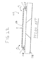
FIG. 12 depicts one such raisedmicrostructure 110 of the prior art. After the oxide is removed leaving theraised microstructure 110, an intrinsic tension will be present within theplate 112. This tension T results from the manufacturing process as well as from the difference between the coefficient of expansion of the material of the raisedmicrostructure 110 and the supportingwafer 116. As shown, the tension T is directed radially outwards. The tension T intrinsic in theplate 112 will result in a moment as shown by arrow M about thebase 118 ofsidewall 114. This moment M results in a tendency of theplate 112 to deflect towards thewafer 116 in the direction of arrow D. This deflection ofplate 112 results in a negative effect on the sensitivity and performance of the microphone. - A number of undesirable means to negate the effects of this intrinsic tension within a thin-film raised microstructure are known in the prior art. Among them are that the composition of the thin film can be adjusted by making it silicon rich to reduce its intrinsic stress levels. However, this Technique has its disadvantages. It results in making the thin film less etch resistant to HF acid, increasing the difficulty and expense of manufacture. An additional solution known in the prior art would be to increase the thickness of the sidewall supporting the raised backplate thereby increasing the sidewall's ability to resist the intrinsic tendency of the thin film to deflect. While this sounds acceptable from a geometry point of view, manufacture of a thick sidewall when the raised microstructure is made using thin film deposition is impractical.
- The object of the present invention is to solve these and other problems.
- One aspect of the present invention results from a realization that a diaphragm has the highest mechanical sensitivity if it is free to move in its own plane. Furthermore, if the diaphragm is resting on a support ring attached to the perforated member, a tight acoustical seal can be achieved leading to a well controlled frequency roll-off of the transducer. Additionally, if a suspension method is chosen such that the suspension only allows the diaphragm to move in its own plane and does not take part in the deflection of the diaphragm to an incident sound pressure wave, complete decoupling from the perforated member can be achieved which reduces the sensitivity to external stresses on the transducer.
- The present invention consists in a raised microstructure for use in a silicon based device, the raised microstructure comprising; a generally planar thin-film plate having a periphery; a ribbed sidewall, the ribbed sidewall including a plurality of ridges and grooves, the ridges and grooves extending about substantially the entire periphery and further being arranged substantially perpendicular to an edge of the thin-film plate defined by the periphery, the ribbed sidewall arranged to support the generally planar thin-film plate along the periphery; wherein the plurality of ridges and grooves of the ribbed sidewall form at least one rib, and wherein at least one rib stiffens the ribbed sidewall. The rib may be of generally arcuate, triangular or rectangular cross section.
-
-
FIG. 1 is an enlarged schematic cross-sectional view taken along the line 1-1 inFIG. 2 of an acoustic transducer with clamped suspension in accordance with the present invention; -
FIG. 2 is a top plan view, partially in phantom, of the acoustic transducer ofFIG. 1 ; -
FIG. 3 is a cross-sectional perspective view of the acoustic transducer ofFIG. 2 taken along line 3-3 ofFIG. 2 ; -
FIG. 4 is an enlarged partial top view, partially in phantom, of an acoustic transducer similar toFIG. 2 wherein the perforated member includes an optionally shaped attach perimeter; -
FIG. 5 is an enlarged schematic cross-sectional view taking along the plane 5-5 inFIG. 6 of an acoustic transducer with high compliance spring suspension in accordance with the present invention; -
FIG. 6 is a top plan view, partially in phantom, of the acoustic transducer ofFIG. 5 ; -
FIG. 7 is a cross-sectional perspective view of the acoustic transducer ofFIG. 6 taken along plane 7-7; -
FIG. 8 is a greatly enlarged partial top view, partially in phantom, of an acoustic transducer similar toFIG. 5 wherein the perforated member includes an optionally shaped attach perimeter; -
FIG. 9 is an electrical circuit for the detection of the change of the microphone capacitance whilst maintaining a constant electrical charge on the microphone; -
FIG. 10 is an electrical circuit for the detection of the change of the microphone capacitance while maintaining a constant electrical potential on the microphone; -
FIG. 11 is a cross-sectional perspective view of the acoustic transducer ofFIG. 4 ; -
FIG. 12 is a cross sectional schematic of a raised microstructure known in the prior art; -
FIG. 13 is a cross sectional perspective view of a raised microstructure embodying the present invention; -
FIG. 14 is a cross section of the raised microstructure ofFIG. 13 ; and -
FIG. 15 is a plan view ofFIG. 13 . - Referring now to the drawings, and particularly to
FIGS. 1-3 , an acoustic transducer in accordance with the present invention is disclosed. Theacoustic transducer 10 includes aconductive diaphragm 12 and aperforated member 40 supported by asubstrate 30 and separated by anair gap 20. A very narrow air gap orwidth 22 exists between thediaphragm 12 andsubstrate 30 allowing the diaphragm to move freely in its plane, thereby relieving any intrinsic stress in the diaphragm material and decoupling the diaphragm from the substrate. A number ofsmall indentations 13 are made in the diaphragm to prevent stiction in the narrow gap between the diaphragm and substrate. The lateral motion of thediaphragm 12 is restricted by asupport structure 41 in theperforated member 40, which also serves to maintain the proper initial spacing between diaphragm and perforated member. Thesupport structure 41 may either be a continuous ring or a plurality of bumps. If thesupport structure 41 is a continuous ring, then diaphragm 12 resting on thesupport structure 41 forms tight acoustical seal, leading to a well controlled low frequency roll-off of the transducer. If thesupport structure 41 is a plurality of bumps, then the acoustical seal can be formed either by limiting the spacing between the bumps, by thenarrow air gap 22, or a combination thereof . - The conducting
diaphragm 12 is electrically insulated from thesubstrate 30 by adielectric layer 31. A conductingelectrode 42 is attached to the non-conductiveperforated member 40. The perforated member contains a number ofopenings 21 through which a sacrificial layer (not shown) between the diaphragm and perforated member is etched during fabrication to form theair gap 20 and which later serve to reduce the acoustic damping of the air in the air gap to provide sufficient bandwidth of the transducer. A number of openings are also made in thediaphragm 12 and theperforated member 40 to form aleakage path 14 which together with the compliance of the back chamber (not shown), on which the transducer will be mounted, forms a high-pass filter resulting in a roll-off frequency low enough not to impede the acoustic function of the transducer and high enough to remove the influence of barometric pressure variations. Theopenings 14 are defined by photo lithographic methods and can therefore be tightly controlled, leading to a well defined low frequency behavior of the transducer. The attachment of the perforatedmember 40 along theperimeter 43 can be varied to reduce the curvature of the perforated member due to intrinsic internal bending moments. The perimeter can be a continuous curved surface (FIGS. 1-3 ) or discontinuous, such as corrugated (FIG. 4 ). Adiscontinuous perimeter 43 provides additional rigidity of the perforatedmember 40 thereby reducing the curvature due to intrinsic bending moments in theperforated member 40. - Turning to
FIGS. 5-7 , an alternative embodiment of an acoustic transducer in accordance with the present invention is depicted. Thetransducer 50 includes aconductive diaphragm 12 and aperforated member 40 supported by asubstrate 30 and separated by anair gap 20. Thediaphragm 12 is attached to the substrate through a number ofsprings 11, which serve to mechanically decouple the diaphragm from the substrate, thereby relieving any intrinsic stress in the diaphragm. Moreover, the diaphragm is released for stress in the substrate and device package. - The lateral motion of the
diaphragm 12 is restricted by asupport structure 41 in theperforated member 40, which also serves to maintain the proper initial spacing between diaphragm andperforated member 40. Thesupport structure 41 may either be a continuous ring or a plurality of bumps. If thesupport structure 41 is a continuous ring, then diaphragm 12 resting on thesupport structure 41 forms tight acoustical seal, leading to a well controlled low frequency roll-off of the transducer. If thesupport structure 41 is a plurality of bumps, then the acoustical seal can be formed by limiting the spacing between the bumps, or by providing a sufficiently long path around the diaphragm and through theperforations 21. - The conducting
diaphragm 12 is electrically insulated from thesubstrate 30 by adielectric layer 31. A conductingelectrode 42 is attached to the non-conductiveperforated member 40. The perforated member contains a number ofopenings 21 through which a sacrificial layer (not shown) between thediaphragm 12 and the perforated member is etched during fabrication to form theair gap 20 and which later serves to reduce the acoustic damping of the air in the air gap to provide sufficient bandwidth of the transducer. A number of openings are made in thesupport structure 41 to form a leakage path 14 (FIG. 6 ) which together with the compliance of the back chamber (not shown) on which the transducer can be mounted forms a high-pass filter resulting in a roll-off frequency low enough not to impede the acoustic function of the transducer and high enough to remove the influence of barometric pressure variations. Theopenings 14 are preferably defined by photo lithographic methods and can therefore be tightly controlled, leading to a well defined low frequency behavior of the transducer. The attachment of the perforated member along theperimeter 43 can be varied to reduce the curvature of the perforated member due to intrinsic internal bending moments. Theperimeter 43 can be smooth (FIGS. 5-7 ) or corrugated (FIGS. 8 and11 ). A corrugated perimeter provides additional rigidity of the perforated member thereby reducing the curvature due to intrinsic bending moments in the perforated member. - In operation, an electrical potential is applied between the
conductive diaphragm 12 and theelectrode 42 on the perforated member. The electrical potential and associated charging of the conductors produces an electrostatic attraction force between the diaphragm and the perforated member. As a result, thefree diaphragm 12 moves toward theperforated member 40 until it rests upon thesupport structure 41, which sets the initial operating point of the transducer with a well definedair gap 20 and acoustic leakage throughpath 14. When subjected to acoustical energy, a pressure difference appears across thediaphragm 12 causing it to deflect towards or away from the perforatedmember 40. The deflection of thediaphragm 12 causes a change of the electrical field, and consequently capacitance, between thediaphragm 12 and theperforated member 40. As a result the electrical capacitance of the transducer is modulated by the acoustical energy. - A method to detect the modulation of capacitance is shown in
FIG. 9 . In thedetection circuit 100, thetransducer 102 is connected to aDC voltage source 101 and a unity-gain amplifier 104 with very high input impedance. Abias resistor 103 ties the DC potential of the amplifier input to ground whereby the DC potential "Vbias" is applied across the transducer. Assuming in this circuit a constant electrical charge on the transducer, a change of transducer capacitance results in a change of electrical potential across the transducer, which is measured by the unity-gain amplifier. - Another method to detect the modulation of capacitance is shown in
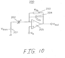
FIG. 10 . In thedetection circuit 200, thetransducer 202 is connected to aDC voltage source 201 and acharge amplifier configuration 205 with afeedback resistor 203 andcapacitor 204. The feedback resistor ensures DC stability of the circuit and maintains the DC level of the input of the amplifier, whereby the DC potential "Vbias-Vb" is applied across the transducer. Assuming in this circuit a constant potential across the transducer, due to the virtual ground principle of the amplifier, a change of capacitance causes a change of charge on the transducer and consequently on the input side of the feedback capacitor leading to an offset between the negative and positive input on the amplifier. The amplifier supplies a mirror charge on output side of the feedback capacitor to remove the offset, resulting in a change of output voltage "Vout." The charge gain in this circuit is set by the ratio between the initial transducer capacitance and the capacitance of the feedback capacitor. An advantage of this detection circuit is that the virtual ground principle of the amplifier eliminates any parasitic capacitance to electrical ground in the transducer, which otherwise attenuate the effect of the dynamic change of the microphone capacitance. However, care should be taken to reduce parasitic capacitances to minimize the of gain of any noise on the signal "Vb" and the inherent amplifier noise. - An embodiment of the raised
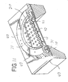
microstructure 110 of the present invention is shown inFIGS. 13 and 14 . The raisedmicrostructure 110 comprises a generally circular thin-film plate orbackplate 112 supported by asidewall 114. - The raised
microstructure 110 is comprised of athin film plate 112 of silicon nitride deposited on top of a sacrificial silicon oxide layer on asilicon wafer 116 using deposition and etching techniques readily and commonly known to those of ordinary skill in the relevant arts. The sacrificial silicon oxide layer has already been removed from the figure for clarity. Thesidewall 114 of the raisedmicrostructure 110 is attached at itsbase 118 to thesilicon wafer 116 and attached at its opposite end to theplate 112. Thesidewall 114 is generally perpendicular toplate 112, but it is noted other angles may be utilized between thesidewall 114 and theplate 112. -
FIG. 15 shows a plan view of the assembly ofFIG. 13 with a surface of thesidewall 114 of the present invention shown in phantom. It can be seen that thesidewall 114 of the present invention as shown inFIGS. 13-15 is ribbed, forming a plurality ofperiodic ridges 120 andgrooves 122. In the preferred embodiment, theridges 120 andgrooves 122 are parallel and equally spaced, forming a corrugated structure. Furthermore, the preferred embodiment utilizesridges 120 andgrooves 122 of a squared cross section. The effect of corrugating the side wall in this manner is to createsegments 124 of thesidewall 114 that are radial, as is the intrinsic tension T of theplate 112. By making portions of thesidewall 114 radial, as is the tension T, thesidewall 114 is stiffened. It has been found that thesidewall 114 of the prior art, which is tangential toplate 112, is easily bent as compared to theradial segments 124 of the present invention. - Other geometries than that shown in
FIGS. 13-15 of the corrugations orridges 120 andgrooves 122 can be imagined and used effectively to increase the sidewall's 114 ability to resist moment M and the geometry depicted in theFIGS. 13-15 is not intended to limit the scope of the present invention. - For example, a generally annular geometry, generally triangular geometry or any combination or variation of these geometries or others could be utilized for the
ridges 122 andgrooves 124. - In the preferred embodiment, the corrugations are radial and hence the
sidewalls 114 are parallel to the tension in thebackplate 112. Furthermore, the sacrificial material is etched in such a way that thesidewalls 114 are sloped with respect to the substrate to allow good step coverage as thethin film backplate 112 is deposited.
Claims (8)
- A raised microstructure (110) for use in a silicon based device, the raised microstructure (110) comprising; a generally planar thin-filmplate (112) having a periphery; and a sidewall (114), characterised in that the sidewall (114) is ribbed and includes a plurality of ridges (120) and grooves (122), the ridges and grooves (120, 122) extending about substantially the entire periphery and further being arranged substantially perpendicular to an edge of the thin-film plate (112) defined by the periphery, the ribbed sidewall (114) arranged to support the generally planar thin-film plate (112) along the periphery; and in that the plurality of ridges and grooves (120, 122) of the ribbed sidewall (114) form at least one rib, and wherein at least one rib stiffens the ribbed sidewall (114).
- The raised microstructure of claim 1 wherein the ridges and grooves (120, 122) of the ribbed sidewall (114) are parallel and equally spaced to form a corrugated sidewall.
- The raised microstructure of claim 1 wherein the rib (120) has a generally arcuate cross section.
- The raised microstructure of claim 1 wherein the rib (120) has a generally triangular cross section.
- The raised microstructure of claim 1 wherein the rib (120) has a generally rectangular cross section.
- The raised microstructure of claim 1 wherein the thin-film plate (112) comprises one plate of a silicon based capacitive transducer.
- The raised microstructure of claim 1 wherein the thin-film plate (112) comprises a rigid backplate of a silicon based microphone.
- The raised microstructure of claim 1 wherein the sidewall (114) substantially completely encloses the area beneath the thin-film plate (112).
Applications Claiming Priority (5)
| Application Number | Priority Date | Filing Date | Title |
|---|---|---|---|
| US63740100A | 2000-08-11 | 2000-08-11 | |
| US637401 | 2000-08-11 | ||
| US910110 | 2001-07-20 | ||
| US09/910,110 US6987859B2 (en) | 2001-07-20 | 2001-07-20 | Raised microstructure of silicon based device |
| EP01959715A EP1310136B1 (en) | 2000-08-11 | 2001-08-10 | Miniature broadband transducer |
Related Parent Applications (1)
| Application Number | Title | Priority Date | Filing Date |
|---|---|---|---|
| EP01959715A Division EP1310136B1 (en) | 2000-08-11 | 2001-08-10 | Miniature broadband transducer |
Publications (3)
| Publication Number | Publication Date |
|---|---|
| EP1469701A2 EP1469701A2 (en) | 2004-10-20 |
| EP1469701A3 EP1469701A3 (en) | 2005-11-16 |
| EP1469701B1 true EP1469701B1 (en) | 2008-04-16 |
Family
ID=27092826
Family Applications (2)
| Application Number | Title | Priority Date | Filing Date |
|---|---|---|---|
| EP01959715A Expired - Lifetime EP1310136B1 (en) | 2000-08-11 | 2001-08-10 | Miniature broadband transducer |
| EP04076015A Expired - Lifetime EP1469701B1 (en) | 2000-08-11 | 2001-08-10 | Raised microstructures |
Family Applications Before (1)
| Application Number | Title | Priority Date | Filing Date |
|---|---|---|---|
| EP01959715A Expired - Lifetime EP1310136B1 (en) | 2000-08-11 | 2001-08-10 | Miniature broadband transducer |
Country Status (9)
| Country | Link |
|---|---|
| EP (2) | EP1310136B1 (en) |
| JP (3) | JP4338395B2 (en) |
| KR (1) | KR100571967B1 (en) |
| CN (2) | CN101867858B (en) |
| AT (2) | ATE392790T1 (en) |
| AU (1) | AU2001281241A1 (en) |
| DE (2) | DE60118208T2 (en) |
| DK (2) | DK1310136T3 (en) |
| WO (1) | WO2002015636A2 (en) |
Cited By (4)
| Publication number | Priority date | Publication date | Assignee | Title |
|---|---|---|---|---|
| US9779716B2 (en) | 2015-12-30 | 2017-10-03 | Knowles Electronics, Llc | Occlusion reduction and active noise reduction based on seal quality |
| US9812149B2 (en) | 2016-01-28 | 2017-11-07 | Knowles Electronics, Llc | Methods and systems for providing consistency in noise reduction during speech and non-speech periods |
| US9830930B2 (en) | 2015-12-30 | 2017-11-28 | Knowles Electronics, Llc | Voice-enhanced awareness mode |
| US9961443B2 (en) | 2015-09-14 | 2018-05-01 | Knowles Electronics, Llc | Microphone signal fusion |
Families Citing this family (115)
| Publication number | Priority date | Publication date | Assignee | Title |
|---|---|---|---|---|
| US6535460B2 (en) | 2000-08-11 | 2003-03-18 | Knowles Electronics, Llc | Miniature broadband acoustic transducer |
| US6987859B2 (en) | 2001-07-20 | 2006-01-17 | Knowles Electronics, Llc. | Raised microstructure of silicon based device |
| US7434305B2 (en) | 2000-11-28 | 2008-10-14 | Knowles Electronics, Llc. | Method of manufacturing a microphone |
| US7166910B2 (en) | 2000-11-28 | 2007-01-23 | Knowles Electronics Llc | Miniature silicon condenser microphone |
| US7439616B2 (en) | 2000-11-28 | 2008-10-21 | Knowles Electronics, Llc | Miniature silicon condenser microphone |
| US8623709B1 (en) | 2000-11-28 | 2014-01-07 | Knowles Electronics, Llc | Methods of manufacture of top port surface mount silicon condenser microphone packages |
| US6859542B2 (en) | 2001-05-31 | 2005-02-22 | Sonion Lyngby A/S | Method of providing a hydrophobic layer and a condenser microphone having such a layer |
| US7023066B2 (en) | 2001-11-20 | 2006-04-04 | Knowles Electronics, Llc. | Silicon microphone |
| KR100437681B1 (en) * | 2002-04-15 | 2004-06-30 | 부전전자부품 주식회사 | Directional microphone |
| DE10238523B4 (en) | 2002-08-22 | 2014-10-02 | Epcos Ag | Encapsulated electronic component and method of manufacture |
| US6781231B2 (en) | 2002-09-10 | 2004-08-24 | Knowles Electronics Llc | Microelectromechanical system package with environmental and interference shield |
| JP2004356707A (en) * | 2003-05-27 | 2004-12-16 | Hosiden Corp | Sound detection mechanism |
| US7030536B2 (en) * | 2003-12-29 | 2006-04-18 | General Electric Company | Micromachined ultrasonic transducer cells having compliant support structure |
| JP4201723B2 (en) * | 2004-02-13 | 2008-12-24 | 東京エレクトロン株式会社 | Capacitance detection type sensor element |
| DE102004020204A1 (en) | 2004-04-22 | 2005-11-10 | Epcos Ag | Encapsulated electrical component and method of manufacture |
| US7329933B2 (en) | 2004-10-29 | 2008-02-12 | Silicon Matrix Pte. Ltd. | Silicon microphone with softly constrained diaphragm |
| US7346178B2 (en) * | 2004-10-29 | 2008-03-18 | Silicon Matrix Pte. Ltd. | Backplateless silicon microphone |
| JP4539450B2 (en) | 2004-11-04 | 2010-09-08 | オムロン株式会社 | Capacitive vibration sensor and manufacturing method thereof |
| KR100685092B1 (en) * | 2005-03-14 | 2007-02-22 | 주식회사 케이이씨 | Micro-phone using Micro Electro Mechanical Systems process and manufacturing method the same |
| US7449356B2 (en) | 2005-04-25 | 2008-11-11 | Analog Devices, Inc. | Process of forming a microphone using support member |
| US7885423B2 (en) | 2005-04-25 | 2011-02-08 | Analog Devices, Inc. | Support apparatus for microphone diaphragm |
| US7825484B2 (en) | 2005-04-25 | 2010-11-02 | Analog Devices, Inc. | Micromachined microphone and multisensor and method for producing same |
| SG127754A1 (en) * | 2005-05-16 | 2006-12-29 | Sensfab Pte Ltd | Silicon microphone |
| DE102005031601B4 (en) * | 2005-07-06 | 2016-03-03 | Robert Bosch Gmbh | Capacitive micromechanical microphone |
| US8351632B2 (en) | 2005-08-23 | 2013-01-08 | Analog Devices, Inc. | Noise mitigating microphone system and method |
| KR20080009735A (en) | 2005-09-09 | 2008-01-29 | 야마하 가부시키가이샤 | Capacitor microphone |
| KR100765149B1 (en) * | 2005-10-05 | 2007-10-15 | 전자부품연구원 | Micro acoustic sensing apparatus and manufacturing thereof |
| KR100785803B1 (en) * | 2005-12-07 | 2007-12-13 | 한국전자통신연구원 | Spring structure embedded microphone, speaker and speech recognition/synthesizing device |
| DE102006001493B4 (en) * | 2006-01-11 | 2007-10-18 | Austriamicrosystems Ag | MEMS sensor and method of manufacture |
| JP5215871B2 (en) * | 2006-01-20 | 2013-06-19 | アナログ デバイシス, インコーポレイテッド | Capacitor microphone diaphragm support device |
| JP4811035B2 (en) * | 2006-01-31 | 2011-11-09 | パナソニック電工株式会社 | Acoustic sensor |
| JP4737721B2 (en) * | 2006-03-10 | 2011-08-03 | ヤマハ株式会社 | Condenser microphone |
| JP4605470B2 (en) * | 2006-03-31 | 2011-01-05 | ヤマハ株式会社 | Condenser microphone |
| JP2007267049A (en) * | 2006-03-29 | 2007-10-11 | Yamaha Corp | Condenser microphone |
| JP4737720B2 (en) * | 2006-03-06 | 2011-08-03 | ヤマハ株式会社 | Diaphragm, manufacturing method thereof, condenser microphone having the diaphragm, and manufacturing method thereof |
| JP2007228345A (en) * | 2006-02-24 | 2007-09-06 | Yamaha Corp | Capacitor microphone |
| JP4737719B2 (en) * | 2006-02-24 | 2011-08-03 | ヤマハ株式会社 | Condenser microphone |
| GB0605576D0 (en) * | 2006-03-20 | 2006-04-26 | Oligon Ltd | MEMS device |
| JP4605544B2 (en) * | 2006-03-29 | 2011-01-05 | ヤマハ株式会社 | Condenser microphone |
| TW200746869A (en) | 2006-03-29 | 2007-12-16 | Yamaha Corp | Condenser microphone |
| US8270634B2 (en) | 2006-07-25 | 2012-09-18 | Analog Devices, Inc. | Multiple microphone system |
| JP4567643B2 (en) * | 2006-08-24 | 2010-10-20 | パナソニック株式会社 | Capacitor and manufacturing method thereof |
| CN101141832B (en) * | 2006-09-06 | 2011-04-20 | 歌尔声学股份有限公司 | Single membrane capacitance type microphone chip |
| JP2010506532A (en) * | 2006-10-11 | 2010-02-25 | メムス テクノロジー ビーエイチディー | Extremely low pressure sensor and method for manufacturing the same |
| JP4144640B2 (en) | 2006-10-13 | 2008-09-03 | オムロン株式会社 | Method for manufacturing vibration sensor |
| US7894622B2 (en) | 2006-10-13 | 2011-02-22 | Merry Electronics Co., Ltd. | Microphone |
| EP1931173B1 (en) | 2006-12-06 | 2011-07-20 | Electronics and Telecommunications Research Institute | Condenser microphone having flexure hinge diaphragm and method of manufacturing the same |
| US8111871B2 (en) | 2007-01-17 | 2012-02-07 | Analog Devices, Inc. | Microphone with pressure relief |
| JP5034692B2 (en) * | 2007-06-04 | 2012-09-26 | オムロン株式会社 | Acoustic sensor |
| JP5029147B2 (en) * | 2007-06-04 | 2012-09-19 | オムロン株式会社 | Acoustic sensor |
| JP5412031B2 (en) * | 2007-07-24 | 2014-02-12 | ローム株式会社 | MEMS sensor |
| GB2452941B (en) * | 2007-09-19 | 2012-04-11 | Wolfson Microelectronics Plc | Mems device and process |
| GB2453105B (en) * | 2007-09-19 | 2011-01-12 | Wolfson Microelectronics Plc | MEMS device and process |
| GB2453104B (en) | 2007-09-19 | 2012-04-25 | Wolfson Microelectronics Plc | Mems device and process |
| JP2009089100A (en) * | 2007-09-28 | 2009-04-23 | Yamaha Corp | Vibrating transducer |
| US20090136064A1 (en) | 2007-09-28 | 2009-05-28 | Yamaha Corporation | Vibration transducer and manufacturing method therefor |
| US8045733B2 (en) * | 2007-10-05 | 2011-10-25 | Shandong Gettop Acoustic Co., Ltd. | Silicon microphone with enhanced impact proof structure using bonding wires |
| KR100932754B1 (en) * | 2007-12-12 | 2009-12-21 | 에스텍 주식회사 | Multifunction speaker |
| US7888754B2 (en) | 2007-12-28 | 2011-02-15 | Yamaha Corporation | MEMS transducer |
| US8327711B2 (en) | 2008-02-20 | 2012-12-11 | Omron Corporation | Electrostatic capacitive vibrating sensor |
| JP5332373B2 (en) | 2008-07-25 | 2013-11-06 | オムロン株式会社 | Capacitance type vibration sensor |
| JP4419103B1 (en) | 2008-08-27 | 2010-02-24 | オムロン株式会社 | Capacitance type vibration sensor |
| JP2010074523A (en) * | 2008-09-18 | 2010-04-02 | Rohm Co Ltd | Method of etching sacrificial layer, method of manufacturing mems device, and mems device |
| JP2010155306A (en) | 2008-12-26 | 2010-07-15 | Panasonic Corp | Microelectromechanical systems (mems) device and method of manufacturing the same |
| GB2467848B (en) * | 2009-02-13 | 2011-01-12 | Wolfson Microelectronics Plc | MEMS device and process |
| US8363860B2 (en) | 2009-03-26 | 2013-01-29 | Analog Devices, Inc. | MEMS microphone with spring suspended backplate |
| EP2239961A1 (en) * | 2009-04-06 | 2010-10-13 | Nxp B.V. | Backplate for microphone |
| DE102009026682A1 (en) | 2009-06-03 | 2010-12-09 | Robert Bosch Gmbh | Component with a micromechanical microphone structure and method for its production |
| JP5513813B2 (en) * | 2009-08-31 | 2014-06-04 | 新日本無線株式会社 | MEMS microphone and manufacturing method thereof |
| CN102056061A (en) * | 2009-10-29 | 2011-05-11 | 苏州敏芯微电子技术有限公司 | Capacitive miniature silicon microphone and manufacturing method thereof |
| DE102010000666A1 (en) * | 2010-01-05 | 2011-07-07 | Robert Bosch GmbH, 70469 | Component with a micromechanical microphone structure and method for its production |
| CN102223591B (en) * | 2010-04-19 | 2015-04-01 | 联华电子股份有限公司 | Wafer level packaging structure of micro electro mechanical system microphone and manufacturing method thereof |
| JP5402823B2 (en) | 2010-05-13 | 2014-01-29 | オムロン株式会社 | Acoustic sensor |
| JP4947220B2 (en) | 2010-05-13 | 2012-06-06 | オムロン株式会社 | Acoustic sensor and microphone |
| JP5400708B2 (en) | 2010-05-27 | 2014-01-29 | オムロン株式会社 | Acoustic sensor, acoustic transducer, microphone using the acoustic transducer, and method of manufacturing the acoustic transducer |
| JP2012070120A (en) * | 2010-09-22 | 2012-04-05 | Panasonic Corp | Sensor |
| CN102740203A (en) * | 2011-04-06 | 2012-10-17 | 美律实业股份有限公司 | Combined micro-electrical-mechanical-system microphone and manufacturing method of same |
| US20120328132A1 (en) * | 2011-06-27 | 2012-12-27 | Yunlong Wang | Perforated Miniature Silicon Microphone |
| CN103999484B (en) | 2011-11-04 | 2017-06-30 | 美商楼氏电子有限公司 | As the embedded-type electric medium and manufacture method of the barrier in acoustic equipment |
| JP5177309B1 (en) * | 2012-01-31 | 2013-04-03 | オムロン株式会社 | Capacitive sensor |
| US9078063B2 (en) | 2012-08-10 | 2015-07-07 | Knowles Electronics, Llc | Microphone assembly with barrier to prevent contaminant infiltration |
| DE102012215251A1 (en) * | 2012-08-28 | 2013-03-21 | Robert Bosch Gmbh | Micro-electro-mechanical systems component e.g. valve component, has anchorage structure setting counter-element under tensile stress so that deflections of counter-element counteract perpendicular to layer planes |
| JP5987572B2 (en) | 2012-09-11 | 2016-09-07 | オムロン株式会社 | Acoustic transducer |
| JP5991475B2 (en) | 2012-09-14 | 2016-09-14 | オムロン株式会社 | Acoustic transducer |
| CN102873020B (en) * | 2012-10-12 | 2015-05-06 | 北京七星华创电子股份有限公司 | Connection cover of mega sound wave energy transducer |
| KR101496817B1 (en) * | 2013-08-09 | 2015-02-27 | 삼성전기주식회사 | Acoustic Transducer |
| JP6179300B2 (en) | 2013-09-13 | 2017-08-16 | オムロン株式会社 | Acoustic transducer and microphone |
| JP6345926B2 (en) * | 2013-10-07 | 2018-06-20 | 新日本無線株式会社 | MEMS device and manufacturing method thereof |
| US20150162523A1 (en) | 2013-12-06 | 2015-06-11 | Murata Manufacturing Co., Ltd. | Piezoelectric device |
| DE102014202009A1 (en) * | 2014-02-05 | 2015-08-06 | Robert Bosch Gmbh | Method and means for regulating the electrical bias on the measuring capacitor of a MEMS sensor element |
| US20150296306A1 (en) * | 2014-04-10 | 2015-10-15 | Knowles Electronics, Llc. | Mems motors having insulated substrates |
| WO2015196468A1 (en) | 2014-06-27 | 2015-12-30 | Goertek Inc. | Silicon microphone with suspended diaphragm and system with the same |
| CN105323687A (en) * | 2014-07-14 | 2016-02-10 | 北京卓锐微技术有限公司 | Silicon capacitance microphone with polycrystalline silicon layer being provided with bulges and preparation method thereof |
| CN104105041B (en) * | 2014-07-31 | 2019-01-04 | 歌尔股份有限公司 | Silicon substrate MEMS microphone and preparation method thereof |
| US9743191B2 (en) | 2014-10-13 | 2017-08-22 | Knowles Electronics, Llc | Acoustic apparatus with diaphragm supported at a discrete number of locations |
| US9872116B2 (en) | 2014-11-24 | 2018-01-16 | Knowles Electronics, Llc | Apparatus and method for detecting earphone removal and insertion |
| US9794661B2 (en) | 2015-08-07 | 2017-10-17 | Knowles Electronics, Llc | Ingress protection for reducing particle infiltration into acoustic chamber of a MEMS microphone package |
| US9859879B2 (en) | 2015-09-11 | 2018-01-02 | Knowles Electronics, Llc | Method and apparatus to clip incoming signals in opposing directions when in an off state |
| CN106841396B (en) * | 2015-12-03 | 2019-05-28 | 中国科学院上海微系统与信息技术研究所 | Silicone base capacitance acoustic emission sensor and preparation method thereof |
| KR101807071B1 (en) * | 2016-10-06 | 2017-12-08 | 현대자동차 주식회사 | Microphone and manufacturing method thereof |
| KR101807069B1 (en) | 2016-10-21 | 2017-12-08 | 현대자동차 주식회사 | Microphone and manufacturing the same |
| JP6930101B2 (en) * | 2016-12-12 | 2021-09-01 | オムロン株式会社 | Acoustic sensors and capacitive transducers |
| KR102322258B1 (en) * | 2017-05-19 | 2021-11-04 | 현대자동차 주식회사 | Microphone and manufacturing method thereof |
| DE102017217151B3 (en) | 2017-09-27 | 2019-01-03 | Robert Bosch Gmbh | Micromechanical sensor |
| JP7067891B2 (en) | 2017-10-18 | 2022-05-16 | Mmiセミコンダクター株式会社 | Transducer |
| US10939214B2 (en) | 2018-10-05 | 2021-03-02 | Knowles Electronics, Llc | Acoustic transducers with a low pressure zone and diaphragms having enhanced compliance |
| DE112019004970T5 (en) | 2018-10-05 | 2021-06-24 | Knowles Electronics, Llc | Microphone device with ingress protection |
| CN112789239A (en) | 2018-10-05 | 2021-05-11 | 美商楼氏电子有限公司 | Method for forming MEMS diaphragm comprising folds |
| CN110657880B (en) * | 2019-09-19 | 2022-05-03 | 天津大学 | Novel hydrophone based on resonant air cavity |
| CN111405444B (en) * | 2020-03-20 | 2022-01-25 | 西人马联合测控(泉州)科技有限公司 | Capacitor microphone with diaphragm with holes and manufacturing method thereof |
| US11528546B2 (en) | 2021-04-05 | 2022-12-13 | Knowles Electronics, Llc | Sealed vacuum MEMS die |
| US11540048B2 (en) | 2021-04-16 | 2022-12-27 | Knowles Electronics, Llc | Reduced noise MEMS device with force feedback |
| US11649161B2 (en) | 2021-07-26 | 2023-05-16 | Knowles Electronics, Llc | Diaphragm assembly with non-uniform pillar distribution |
| US11772961B2 (en) | 2021-08-26 | 2023-10-03 | Knowles Electronics, Llc | MEMS device with perimeter barometric relief pierce |
| US11780726B2 (en) | 2021-11-03 | 2023-10-10 | Knowles Electronics, Llc | Dual-diaphragm assembly having center constraint |
Family Cites Families (10)
| Publication number | Priority date | Publication date | Assignee | Title |
|---|---|---|---|---|
| US4360955A (en) * | 1978-05-08 | 1982-11-30 | Barry Block | Method of making a capacitive force transducer |
| JPS5938621A (en) * | 1982-08-27 | 1984-03-02 | Nissan Motor Co Ltd | Analyzing device for vibration |
| JPS6055655A (en) * | 1983-09-07 | 1985-03-30 | Nissan Motor Co Ltd | Semiconductor device having beam structure |
| JPS61105861A (en) * | 1985-06-05 | 1986-05-23 | Nissan Motor Co Ltd | Semiconductor device with beam structure |
| JPH0726887B2 (en) * | 1986-05-31 | 1995-03-29 | 株式会社堀場製作所 | Condenser Microphone type detector diaphragm |
| NL8702589A (en) * | 1987-10-30 | 1989-05-16 | Microtel Bv | ELECTRO-ACOUSTIC TRANSDUCENT OF THE KIND OF ELECTRET, AND A METHOD FOR MANUFACTURING SUCH TRANSDUCER. |
| JPH05172843A (en) * | 1991-12-25 | 1993-07-13 | Omron Corp | Semiconductor acceleration sensor |
| DK0561566T3 (en) * | 1992-03-18 | 2000-03-27 | Knowles Electronics Llc | Solid state condenser microphone |
| US5452268A (en) * | 1994-08-12 | 1995-09-19 | The Charles Stark Draper Laboratory, Inc. | Acoustic transducer with improved low frequency response |
| JP3472493B2 (en) * | 1998-11-30 | 2003-12-02 | ホシデン株式会社 | Semiconductor electret condenser microphone |
-
2001
- 2001-08-10 DE DE60118208T patent/DE60118208T2/en not_active Expired - Lifetime
- 2001-08-10 DE DE60133679T patent/DE60133679T2/en not_active Expired - Lifetime
- 2001-08-10 DK DK01959715T patent/DK1310136T3/en active
- 2001-08-10 DK DK04076015T patent/DK1469701T3/en active
- 2001-08-10 KR KR1020037002017A patent/KR100571967B1/en not_active IP Right Cessation
- 2001-08-10 AT AT04076015T patent/ATE392790T1/en not_active IP Right Cessation
- 2001-08-10 CN CN2010102062254A patent/CN101867858B/en not_active Expired - Lifetime
- 2001-08-10 CN CN018140300A patent/CN1498513B/en not_active Expired - Lifetime
- 2001-08-10 WO PCT/US2001/025184 patent/WO2002015636A2/en active IP Right Grant
- 2001-08-10 AT AT01959715T patent/ATE321429T1/en not_active IP Right Cessation
- 2001-08-10 JP JP2002519372A patent/JP4338395B2/en not_active Expired - Fee Related
- 2001-08-10 EP EP01959715A patent/EP1310136B1/en not_active Expired - Lifetime
- 2001-08-10 EP EP04076015A patent/EP1469701B1/en not_active Expired - Lifetime
- 2001-08-10 AU AU2001281241A patent/AU2001281241A1/en not_active Abandoned
-
2006
- 2006-11-06 JP JP2006300831A patent/JP2007116721A/en active Pending
-
2009
- 2009-04-01 JP JP2009088945A patent/JP5049312B2/en not_active Expired - Fee Related
Cited By (4)
| Publication number | Priority date | Publication date | Assignee | Title |
|---|---|---|---|---|
| US9961443B2 (en) | 2015-09-14 | 2018-05-01 | Knowles Electronics, Llc | Microphone signal fusion |
| US9779716B2 (en) | 2015-12-30 | 2017-10-03 | Knowles Electronics, Llc | Occlusion reduction and active noise reduction based on seal quality |
| US9830930B2 (en) | 2015-12-30 | 2017-11-28 | Knowles Electronics, Llc | Voice-enhanced awareness mode |
| US9812149B2 (en) | 2016-01-28 | 2017-11-07 | Knowles Electronics, Llc | Methods and systems for providing consistency in noise reduction during speech and non-speech periods |
Also Published As
| Publication number | Publication date |
|---|---|
| CN101867858A (en) | 2010-10-20 |
| DE60118208T2 (en) | 2007-04-12 |
| ATE321429T1 (en) | 2006-04-15 |
| DK1469701T3 (en) | 2008-08-18 |
| DK1310136T3 (en) | 2006-07-31 |
| JP4338395B2 (en) | 2009-10-07 |
| JP2007116721A (en) | 2007-05-10 |
| DE60133679D1 (en) | 2008-05-29 |
| WO2002015636A3 (en) | 2002-10-24 |
| CN101867858B (en) | 2012-02-22 |
| DE60133679T2 (en) | 2009-06-10 |
| EP1469701A3 (en) | 2005-11-16 |
| WO2002015636A2 (en) | 2002-02-21 |
| CN1498513B (en) | 2010-07-14 |
| CN1498513A (en) | 2004-05-19 |
| JP5049312B2 (en) | 2012-10-17 |
| EP1310136A2 (en) | 2003-05-14 |
| JP2009153203A (en) | 2009-07-09 |
| KR100571967B1 (en) | 2006-04-18 |
| ATE392790T1 (en) | 2008-05-15 |
| JP2004506394A (en) | 2004-02-26 |
| AU2001281241A1 (en) | 2002-02-25 |
| EP1469701A2 (en) | 2004-10-20 |
| EP1310136B1 (en) | 2006-03-22 |
| KR20030033026A (en) | 2003-04-26 |
| DE60118208D1 (en) | 2006-05-11 |
Similar Documents
| Publication | Publication Date | Title |
|---|---|---|
| EP1469701B1 (en) | Raised microstructures | |
| US6535460B2 (en) | Miniature broadband acoustic transducer | |
| US6987859B2 (en) | Raised microstructure of silicon based device | |
| US8644528B2 (en) | Microfabricated microphone | |
| JP3556676B2 (en) | Small silicon condenser microphone | |
| US9516421B1 (en) | Acoustic sensing apparatus and method of manufacturing the same | |
| US20060280319A1 (en) | Micromachined Capacitive Microphone | |
| US20080247573A1 (en) | Miniature capacitive acoustic sensor with stress-relieved actively clamped diaphragm | |
| KR101887537B1 (en) | Acoustic sensor and manufacturing method thereof | |
| US11496820B2 (en) | MEMS device with quadrilateral trench and insert | |
| TW201808783A (en) | MEMS device and process | |
| CN111263282B (en) | Condenser microphone and manufacturing method thereof | |
| KR101816253B1 (en) | Voice transmitting device and manufacturing method thereof | |
| KR102035242B1 (en) | Sound transmitting device and manufacturing method thereof | |
| JP2008022501A (en) | Capacitor microphone and its manufacturing method | |
| US20190062146A1 (en) | Mems devices and processes | |
| US20210314718A1 (en) | Process of fabricating lateral mode capacitive microphone including a capacitor plate with sandwich structure | |
| KR102350898B1 (en) | Method for forming mems electrode | |
| US10993044B2 (en) | MEMS device with continuous looped insert and trench | |
| US20230312335A1 (en) | Mems transducer | |
| KR20230125678A (en) | Condenser microphone | |
| GB2563090A (en) | MEMS devices and processes |
Legal Events
| Date | Code | Title | Description |
|---|---|---|---|
| PUAI | Public reference made under article 153(3) epc to a published international application that has entered the european phase |
Free format text: ORIGINAL CODE: 0009012 |
|
| 17P | Request for examination filed |
Effective date: 20040420 |
|
| AC | Divisional application: reference to earlier application |
Ref document number: 1310136 Country of ref document: EP Kind code of ref document: P |
|
| AK | Designated contracting states |
Kind code of ref document: A2 Designated state(s): AT BE CH CY DE DK ES FI FR GB GR IE IT LI LU MC NL PT SE TR |
|
| PUAL | Search report despatched |
Free format text: ORIGINAL CODE: 0009013 |
|
| AK | Designated contracting states |
Kind code of ref document: A3 Designated state(s): AT BE CH CY DE DK ES FI FR GB GR IE IT LI LU MC NL PT SE TR |
|
| AKX | Designation fees paid |
Designated state(s): AT BE CH CY DE DK ES FI FR GB GR IE IT LI LU MC NL PT SE TR |
|
| 17Q | First examination report despatched |
Effective date: 20060706 |
|
| GRAP | Despatch of communication of intention to grant a patent |
Free format text: ORIGINAL CODE: EPIDOSNIGR1 |
|
| GRAS | Grant fee paid |
Free format text: ORIGINAL CODE: EPIDOSNIGR3 |
|
| GRAA | (expected) grant |
Free format text: ORIGINAL CODE: 0009210 |
|
| AC | Divisional application: reference to earlier application |
Ref document number: 1310136 Country of ref document: EP Kind code of ref document: P |
|
| AK | Designated contracting states |
Kind code of ref document: B1 Designated state(s): AT BE CH CY DE DK ES FI FR GB GR IE IT LI LU MC NL PT SE TR |
|
| REG | Reference to a national code |
Ref country code: CH Ref legal event code: EP |
|
| REG | Reference to a national code |
Ref country code: IE Ref legal event code: FG4D |
|
| REF | Corresponds to: |
Ref document number: 60133679 Country of ref document: DE Date of ref document: 20080529 Kind code of ref document: P |
|
| REG | Reference to a national code |
Ref country code: DK Ref legal event code: T3 |
|
| NLR4 | Nl: receipt of corrected translation in the netherlands language at the initiative of the proprietor of the patent | ||
| PG25 | Lapsed in a contracting state [announced via postgrant information from national office to epo] |
Ref country code: PT Free format text: LAPSE BECAUSE OF FAILURE TO SUBMIT A TRANSLATION OF THE DESCRIPTION OR TO PAY THE FEE WITHIN THE PRESCRIBED TIME-LIMIT Effective date: 20080916 Ref country code: FI Free format text: LAPSE BECAUSE OF FAILURE TO SUBMIT A TRANSLATION OF THE DESCRIPTION OR TO PAY THE FEE WITHIN THE PRESCRIBED TIME-LIMIT Effective date: 20080416 Ref country code: ES Free format text: LAPSE BECAUSE OF FAILURE TO SUBMIT A TRANSLATION OF THE DESCRIPTION OR TO PAY THE FEE WITHIN THE PRESCRIBED TIME-LIMIT Effective date: 20080727 |
|
| PG25 | Lapsed in a contracting state [announced via postgrant information from national office to epo] |
Ref country code: AT Free format text: LAPSE BECAUSE OF FAILURE TO SUBMIT A TRANSLATION OF THE DESCRIPTION OR TO PAY THE FEE WITHIN THE PRESCRIBED TIME-LIMIT Effective date: 20080416 |
|
| PG25 | Lapsed in a contracting state [announced via postgrant information from national office to epo] |
Ref country code: SE Free format text: LAPSE BECAUSE OF FAILURE TO SUBMIT A TRANSLATION OF THE DESCRIPTION OR TO PAY THE FEE WITHIN THE PRESCRIBED TIME-LIMIT Effective date: 20080716 |
|
| PLBE | No opposition filed within time limit |
Free format text: ORIGINAL CODE: 0009261 |
|
| STAA | Information on the status of an ep patent application or granted ep patent |
Free format text: STATUS: NO OPPOSITION FILED WITHIN TIME LIMIT |
|
| EN | Fr: translation not filed | ||
| PG25 | Lapsed in a contracting state [announced via postgrant information from national office to epo] |
Ref country code: BE Free format text: LAPSE BECAUSE OF FAILURE TO SUBMIT A TRANSLATION OF THE DESCRIPTION OR TO PAY THE FEE WITHIN THE PRESCRIBED TIME-LIMIT Effective date: 20080416 |
|
| 26N | No opposition filed |
Effective date: 20090119 |
|
| PG25 | Lapsed in a contracting state [announced via postgrant information from national office to epo] |
Ref country code: MC Free format text: LAPSE BECAUSE OF NON-PAYMENT OF DUE FEES Effective date: 20080831 |
|
| REG | Reference to a national code |
Ref country code: CH Ref legal event code: PL |
|
| PG25 | Lapsed in a contracting state [announced via postgrant information from national office to epo] |
Ref country code: LI Free format text: LAPSE BECAUSE OF NON-PAYMENT OF DUE FEES Effective date: 20080831 Ref country code: CH Free format text: LAPSE BECAUSE OF NON-PAYMENT OF DUE FEES Effective date: 20080831 |
|
| PG25 | Lapsed in a contracting state [announced via postgrant information from national office to epo] |
Ref country code: IE Free format text: LAPSE BECAUSE OF NON-PAYMENT OF DUE FEES Effective date: 20080811 |
|
| PG25 | Lapsed in a contracting state [announced via postgrant information from national office to epo] |
Ref country code: IT Free format text: LAPSE BECAUSE OF FAILURE TO SUBMIT A TRANSLATION OF THE DESCRIPTION OR TO PAY THE FEE WITHIN THE PRESCRIBED TIME-LIMIT Effective date: 20080416 |
|
| PG25 | Lapsed in a contracting state [announced via postgrant information from national office to epo] |
Ref country code: CY Free format text: LAPSE BECAUSE OF FAILURE TO SUBMIT A TRANSLATION OF THE DESCRIPTION OR TO PAY THE FEE WITHIN THE PRESCRIBED TIME-LIMIT Effective date: 20080416 |
|
| PG25 | Lapsed in a contracting state [announced via postgrant information from national office to epo] |
Ref country code: LU Free format text: LAPSE BECAUSE OF NON-PAYMENT OF DUE FEES Effective date: 20080810 |
|
| PG25 | Lapsed in a contracting state [announced via postgrant information from national office to epo] |
Ref country code: TR Free format text: LAPSE BECAUSE OF FAILURE TO SUBMIT A TRANSLATION OF THE DESCRIPTION OR TO PAY THE FEE WITHIN THE PRESCRIBED TIME-LIMIT Effective date: 20080416 |
|
| PG25 | Lapsed in a contracting state [announced via postgrant information from national office to epo] |
Ref country code: GR Free format text: LAPSE BECAUSE OF FAILURE TO SUBMIT A TRANSLATION OF THE DESCRIPTION OR TO PAY THE FEE WITHIN THE PRESCRIBED TIME-LIMIT Effective date: 20080717 |
|
| PGFP | Annual fee paid to national office [announced via postgrant information from national office to epo] |
Ref country code: GB Payment date: 20110825 Year of fee payment: 11 |
|
| PG25 | Lapsed in a contracting state [announced via postgrant information from national office to epo] |
Ref country code: FR Free format text: LAPSE BECAUSE OF FAILURE TO SUBMIT A TRANSLATION OF THE DESCRIPTION OR TO PAY THE FEE WITHIN THE PRESCRIBED TIME-LIMIT Effective date: 20090227 |
|
| GBPC | Gb: european patent ceased through non-payment of renewal fee |
Effective date: 20120810 |
|
| PG25 | Lapsed in a contracting state [announced via postgrant information from national office to epo] |
Ref country code: GB Free format text: LAPSE BECAUSE OF NON-PAYMENT OF DUE FEES Effective date: 20120810 |
|
| PGFP | Annual fee paid to national office [announced via postgrant information from national office to epo] |
Ref country code: NL Payment date: 20150826 Year of fee payment: 15 |
|
| PGFP | Annual fee paid to national office [announced via postgrant information from national office to epo] |
Ref country code: DK Payment date: 20150825 Year of fee payment: 15 |
|
| REG | Reference to a national code |
Ref country code: DK Ref legal event code: EBP Effective date: 20160831 |
|
| REG | Reference to a national code |
Ref country code: NL Ref legal event code: MM Effective date: 20160901 |
|
| PG25 | Lapsed in a contracting state [announced via postgrant information from national office to epo] |
Ref country code: NL Free format text: LAPSE BECAUSE OF NON-PAYMENT OF DUE FEES Effective date: 20160901 |
|
| PG25 | Lapsed in a contracting state [announced via postgrant information from national office to epo] |
Ref country code: DK Free format text: LAPSE BECAUSE OF NON-PAYMENT OF DUE FEES Effective date: 20160831 |
|
| PGFP | Annual fee paid to national office [announced via postgrant information from national office to epo] |
Ref country code: DE Payment date: 20201029 Year of fee payment: 20 |
|
| REG | Reference to a national code |
Ref country code: DE Ref legal event code: R071 Ref document number: 60133679 Country of ref document: DE |