JP3556676B2 - Small silicon condenser microphone - Google Patents
Small silicon condenser microphone Download PDFInfo
- Publication number
- JP3556676B2 JP3556676B2 JP53684198A JP53684198A JP3556676B2 JP 3556676 B2 JP3556676 B2 JP 3556676B2 JP 53684198 A JP53684198 A JP 53684198A JP 53684198 A JP53684198 A JP 53684198A JP 3556676 B2 JP3556676 B2 JP 3556676B2
- Authority
- JP
- Japan
- Prior art keywords
- diaphragm
- microphone
- support structure
- distal end
- silicon
- Prior art date
- Legal status (The legal status is an assumption and is not a legal conclusion. Google has not performed a legal analysis and makes no representation as to the accuracy of the status listed.)
- Expired - Fee Related
Links
Images


Classifications
-
- B—PERFORMING OPERATIONS; TRANSPORTING
- B81—MICROSTRUCTURAL TECHNOLOGY
- B81B—MICROSTRUCTURAL DEVICES OR SYSTEMS, e.g. MICROMECHANICAL DEVICES
- B81B3/00—Devices comprising flexible or deformable elements, e.g. comprising elastic tongues or membranes
- B81B3/0064—Constitution or structural means for improving or controlling the physical properties of a device
- B81B3/0067—Mechanical properties
- B81B3/0072—For controlling internal stress or strain in moving or flexible elements, e.g. stress compensating layers
-
- G—PHYSICS
- G01—MEASURING; TESTING
- G01H—MEASUREMENT OF MECHANICAL VIBRATIONS OR ULTRASONIC, SONIC OR INFRASONIC WAVES
- G01H11/00—Measuring mechanical vibrations or ultrasonic, sonic or infrasonic waves by detecting changes in electric or magnetic properties
- G01H11/06—Measuring mechanical vibrations or ultrasonic, sonic or infrasonic waves by detecting changes in electric or magnetic properties by electric means
-
- H—ELECTRICITY
- H04—ELECTRIC COMMUNICATION TECHNIQUE
- H04R—LOUDSPEAKERS, MICROPHONES, GRAMOPHONE PICK-UPS OR LIKE ACOUSTIC ELECTROMECHANICAL TRANSDUCERS; DEAF-AID SETS; PUBLIC ADDRESS SYSTEMS
- H04R19/00—Electrostatic transducers
- H04R19/005—Electrostatic transducers using semiconductor materials
-
- H—ELECTRICITY
- H04—ELECTRIC COMMUNICATION TECHNIQUE
- H04R—LOUDSPEAKERS, MICROPHONES, GRAMOPHONE PICK-UPS OR LIKE ACOUSTIC ELECTROMECHANICAL TRANSDUCERS; DEAF-AID SETS; PUBLIC ADDRESS SYSTEMS
- H04R7/00—Diaphragms for electromechanical transducers; Cones
- H04R7/16—Mounting or tensioning of diaphragms or cones
-
- B—PERFORMING OPERATIONS; TRANSPORTING
- B81—MICROSTRUCTURAL TECHNOLOGY
- B81B—MICROSTRUCTURAL DEVICES OR SYSTEMS, e.g. MICROMECHANICAL DEVICES
- B81B2201/00—Specific applications of microelectromechanical systems
- B81B2201/02—Sensors
- B81B2201/0257—Microphones or microspeakers
-
- B—PERFORMING OPERATIONS; TRANSPORTING
- B81—MICROSTRUCTURAL TECHNOLOGY
- B81B—MICROSTRUCTURAL DEVICES OR SYSTEMS, e.g. MICROMECHANICAL DEVICES
- B81B2203/00—Basic microelectromechanical structures
- B81B2203/01—Suspended structures, i.e. structures allowing a movement
- B81B2203/0127—Diaphragms, i.e. structures separating two media that can control the passage from one medium to another; Membranes, i.e. diaphragms with filtering function
-
- H—ELECTRICITY
- H04—ELECTRIC COMMUNICATION TECHNIQUE
- H04R—LOUDSPEAKERS, MICROPHONES, GRAMOPHONE PICK-UPS OR LIKE ACOUSTIC ELECTROMECHANICAL TRANSDUCERS; DEAF-AID SETS; PUBLIC ADDRESS SYSTEMS
- H04R31/00—Apparatus or processes specially adapted for the manufacture of transducers or diaphragms therefor
- H04R31/006—Interconnection of transducer parts
Abstract
Description
技術分野
本発明は、CMOS回路系に集積化することができる小型シリコンコンデンサマイクロホンに関する。
背景の従来技術
CMOS回路系に集積化することができる小型シリコンコンデンサマイクロホンは、最小体積において高感度と低ノイズとを得るために幾つかのトレードオフを必要とする。典型的には、コンデンサマイクロホンは、4つの要素、すなわち、固定有孔バックプレート、高コンプライアンス可動ダイヤフラム(このバックプレートとダイヤフラムは共に可変エアギャップコンデンサの2つの電極を形成する)、電圧バイアス源、及び、緩衝増幅器から構成されている。
上記ダイヤフラムは、高コンプライアンスでありかつ上記バックプレートに対して正確に位置決めされなければならず、一方、上記バックプレートは、定置状態のままでありかつそのバックプレートを通過する空気流に対して最小限の抵抗しか与えないものでなければならない。集積回路材料を使用してサイズ1mm未満のマイクロホンの形でこれらの特徴を全て実現することは、これまで3つの側面において困難な課題であった。第1に、現在までのシリコンベースの小型コンデンサマイクロホンは、その最大たわみがダイヤフラムの中央で生じる、周囲フレームによって保持されたダイヤフラムを使用してきた。この構成では、ダイヤフラム材料内の除去されることのない応力が、(その応力が、ダイヤフラムを剛化させる引張り応力である場合には)ダイヤフラムのコンプライアンスの低下を生じさせるか、または、(その応力がダイヤフラムを座屈させる圧縮応力である場合には)位置決め精度の低下を生じさせる。集積回路薄膜における典型的な応力レベルは、完成ダイヤフラム内から除去されない場合には、過剰な剛化または座屈のためにダイヤフラムが使用不可能になるレベルよりも何倍も高いレベルである。
1mm未満の大きさのダイヤフラムの第2の問題点は、ダイヤグラムの材料と厚さとが決まっている場合には、ダイヤフラムのサイズが小さければ小さいほどコンプライアンスが極めて急激に低下する傾向があるということである。ダイヤフラムコンプライアンスの単位を単位圧力当たりの直線たわみとする場合に、このコンプライアンスは、ダイヤフラムサイズの4乗とみなされる。具体例としては、ダイヤフラムの材料と厚さと形状が同一に保たれる場合には、ダイヤフラム直径を半分に削減することは、ダイヤグラムコンプライアンスをその以前の値の16分の1に低下させると推定される。
サイズ1mm未満のマイクロホンの小型化における第3の問題点は、ダイヤフラム変位に対する機械的減衰を小さい度合いに維持することである。緩衝増幅器の入力を効果的に駆動することが可能な範囲内にコンデンサ容量を保つためには、その構造がより小さくされるのに応じて、エアギャップがより小さくされなければならない(装置サイズの2乗の逆数として概算される)。残念なことに、エアギャップが小さくされればされるほど、ダイヤフラムとバックプレートとの間に閉じ込められている空気の粘性流に起因する減衰効果が、エアギャップのサイズの3乗の逆数として変化し、急激に増大する。その最終的な結果として、機械的減衰が、装置サイズの6乗の逆数の形で極めて急激に増大する傾向がある。この減衰は周波数応答に悪影響を与え、すでに確立されている理論にしたがえば、マイクロホン出力の雑音の原因となるマイクロホン構造内での圧力変動を生じさせる。
小型コンデンサマイクロホンのダイヤフラムにおける過剰応力の問題を回避するために、これまでに様々な解決策が提案されてきた。こうした解決策は、その解決策がダイヤグラム材料に焦点を当てているか、または、ダイヤフラム構造に焦点を当てているかによって、分類されることが可能である。材料の側面では、BergquistとRudolfのTransducers 91,Proceedings of the International Conference on Solid−State Sensors and Actuators(IEEE,New York,1991)pp.266−269が、単結晶シリコンで同様に形成されているダイヤフラム支持体に対する応力格差の発生を最小限に抑えるための、ダイヤフラム材料としての単結晶シリコンを開示している。
Hoshinoの米国特許第4,571,661号は、半導体基部と、その半導体基部に固定されている一方の端部と振動可能な自由端部とを有する可動レバーとを含む、半導体振動検出装置を開示している。しかし、Hoshinoは、流体伝導音圧に対して応答しかつ支持構造の開口の一部分の上に延びている薄膜カンチレバー構造については、開示または示唆し損なっている。
Bernsteinの米国特許第5,146,453号は、パターン成形シリコンばねによってその周囲において支持されている単結晶シリコンダイヤフラムから成る全シリコン構造を開示している。
ダイヤフラム構造の側面では、Loeppertの米国特許第5,490,220号に、自由プレートダイヤフラム構成が開示されており、そのダイヤフラムはそのフレームから分離させられており、かつ、一組の横方向拘束手段だけによって保持されている。Loeppertによれば、ダイヤフラムとそのフレームとの間の材料の不一致にも係わらず、材料応力が完成ダイヤフラム内で完全に除去される。
PCT国際公開WO 95/34917は、ピエゾ電気カンチレバー圧力変換器を開示している。あるいは、この変換器が、磁気ひずみ変換器、ピエゾ抵抗変換器、または、熱変換器であることも可能である。
しかし、上記解決策のいずれにおいても、製造プロセスにおいて良好な性能を維持しながら、この特有の薄膜の応力問題を解決することは不可能である。
本発明は、こうした問題とその他の問題との解決を可能にする。
発明の要約
本発明の目的は、ダイヤフラムの形状がカンチレバーを基本としており、かつ、1mm未満のサイズのマイクロホンに適している別のバックプレート通気構造が使用される、従来とは別のダイヤフラム/バックプレート構造を提供することである。こうしたマイクロホンは、超音波用途、オーディオ用途、および、音声変換用途に使用することができる。
カンチレバー形態においては、ダイヤフラム材料の応力が、自由プレートに関連した保持拘束手段の必要なしに、自由プレート構造の場合と概ね同じ程度まで最終ダイヤフラム構造内で除去される。これに加えて、カンチレバー構造のコンプライアンスは、材料とスパンと厚さが同一である端縁締付けダイヤフラムのコンプライアンスに比べて百倍以上大きく、このことが、サイズ1mm未満のダイヤフラムにおけるコンプライアンスに起因する上記問題点にも係わらず、より小型の装置の設計を容易にする。
このダイヤフラムは、バックプレートと、バックプレート電圧バイアスのため集積CMOS回路系と、緩衝増幅器と共に、単一のシリコンウェーハ上に形成されることが可能である。幾つかの実施形態が下記に示されている。機械的減衰を最小限に抑えるためのコンデンサエアギャップの通気方法は、個々の実施形態の状況に応じて決定され、したがって、個々の場合に状況に応じて与えられる。最終的な結果は、マイクロホンのサイズと感度における利点を提供する解決策であり、このことは当業者には容易に明らかである。
本発明の他の特徴と利点とが、次の添付図面を参照して説明される以下の詳述から明らかになるだろう。
【図面の簡単な説明】
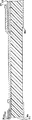
図1は、本発明にしたがって作られるシリコンコンデンサマイクロホンの第1の実施形態の斜視図である。
図1aは、本発明にしたがって作られるシリコンコンデンサマイクロホンの第2の実施形態の斜視図である。
図2から図9は、図1のマイクロホンの製造の連続段階を示す断面図である。
図6a、図6b、図7a、図8a、図9a、図9bは、図1aのマイクロホンの製造の連続段階を示す断面図である。
図10は、本発明にしたがって作られるシリコンコンデンサマイクロホンの第3の実施形態の斜視図である。
図11と図12は、図10のマイクロホンの製造の連続段階を示す断面図である。
図13は、本発明にしたがって作られるシリコンコンデンサマイクロホンの第4の実施形態の斜視図である。
図13aは、ダイヤフラムを省略した、図13のマイクロホンの平面図である。
図13bと図13cは、図13aのマイクロホンの断面図である。
図13dは、ダイヤフラムを含む、図13aのマイクロホンの平面図である。
図14と図15は、図13のマイクロホンの製造の連続段階を示す断面図である。
図16は、本発明の第4の実施形態の変形例のウェブ構造の平面図である。
図16aは、本発明の第4の実施形態の変形例の平面図である。
図16bと図16cは、図16aのマイクロホンの断面図である。
図17aは、第4の実施形態のマイクロホンと共に使用するための過圧止め構造の平面図である。
図17bは、図17aの過圧止め構造の断面図である。
詳細な説明
本発明は様々な形態の実施形態として具体化されることが可能であり、本発明の好ましい実施形態が添付画面に示され下記説明において詳述されているが、本明細書における本発明の開示内容が本発明の原理の例示であるとみなされるべきであることと、本明細書に示されている実施形態に本発明の広範な側面を限定することは意図されていないということとを理解されたい。
シリコンコンデンサマイクロホン10のためのカンチレバー設計が図1に示されている。マイクロホン10は、基部端縁すなわち固定端縁12aにおいて支持構造すなわちフレーム12に固定されておりかつ末端端縁12bを含む他の3つの端縁上では自由であるダイヤフラム12を含む。したがって、ダイヤフラム12の堅さは、ダイヤフラム12の厚さと材料特性とによって決定されるのであって、処理加工時にダイヤフラム12内に発生させられる応力によっては決定されない。コンデンサ14が、固定端縁12aから距離をおいたダイヤフラムの末端端縁12bの付近に配置されており、この場所では、音声圧力に起因するダイヤフラム12の最大たわみが生じる。
図2を参照すると、この図に示されているように、本発明では、基板16上における他の構成要素(図示されていない)のCMOS処理加工中に、両面研摩シリコンウェーハであることが好ましい基板16上にマイクロホン10が形成される。CMOS処理加工中に、フィールド酸化物18によって周囲を囲まれた活性区域18aが標準LOCOSプロセスによって形成され、最終的にダイヤフラム12がそこに配置されることになる。公知であるように、LOCOSプロセスは、基板16の背面上に窒化物層18bも生じさせる。この窒化物層18bは、LOCOSプロセスの完了時に基板16の背面上に残される。
図3を参照すると、この図に示されているように、低温酸化物層20がウェーハ16の表面全体に推積される。CMOSプロセスでは、酸化物層20が、ポリシリコンゲートとアルミニウムインタコネクト(図示されていない)との間の誘電体として、ウェーハ表面の概ね全体上に残されることが一般的である。アルミニウムインタコネクトは、ウェーハ16上の他の位置に形成される回路を接続するために使用される。その後で、裸シリコン基板16を露出させるために、酸化物層20の一部分が除去される。
同様に、CMOSプロセスでは、低温酸化物20とアルミニウムインタコネクト層とを保護するために、ウェーハ表面の概ね全体に窒化ケイ素パッシベーション層22が残されることが一般的である。図4に示されているように、ウェーハ16上に他の位置のCMOS回路区域内において通常の保護を与えるために窒化ケイ素パッシベーション層22がパターン形成されるが、上記と同様に、ダイヤフラム12が形成されることになっている区域内ではシリコン基板16を露出させるために、窒化ケイ素パッシベーション層22が部分的に除去される。したがって、窒化ケイ素パッシベーション層22が、下記の微細加工段階において、水酸化カリウム(KOH)であることが好ましい異方性エッチング剤からCMOS区域を保護するための障壁を形成する。窒化物背面層18bも、下記の最終微細加工段階のためのエッチングマスクを形成するようにパターン形成される。
コンデンサ14は、固定電極14aすなわちバックプレートと、可動電極14bとを含む。図5を参照すると、この図に示されているように、固定電極14aを形成するために、厚さが0.1ミクロンから0.2ミクロンの範囲内の、クロムであることが好ましい金属層が堆積されて、パターン形成されている。
図6を参照すると、この図に示されているように、厚さが約4ミクロンの、アルミニウムであることが好ましい犠牲層24が、堆積されて、パターン形成される。コンデンサ14の固定電極14aと可動電極14bとの間にギャップを形成するために、この犠牲層24は最終的には除去されることになる。
図7を参照すると、この図に示されているように、典型的には厚さ1ミクロンである窒化ケイ素ダイヤフラム層26が堆積され、パターン形成される。
図8を参照すると、この図に示されているように、可動電極14bを形成するために、厚さ約0.02ミクロンの、好ましくはクロムである金属層が、窒化ケイ素ダイヤフラム層26上に堆積されてパターン形成される。
0.02ミクロンの厚さが、応力に関する考慮事項とコンダクタンスに関する考慮事項との間の適切なバランスを与えるものとして使用される。より薄い層の場合には、より低いコンダクタンスが得られるが、応力に関してはより劣った結果をもたらすだろう。
明確には示されていないが、ウェーハ16上のアルミニウムボンディングパッドを保護するために、チタン/タングステン合金層と、その次に、金層とが堆積されて、パターン形成される。
最終微細加工段階が図9に示されている。この段階では、ウェーハ全体が異方性エッチング剤(好ましくは、水酸化カリウム(KOH))でエッチングされる。この段階は、マイクロホン10の可動要素と固定要素との間にコンデンサギャップ28を形成し、かつ、ダイヤフラム12の下に穴30を形成する。
図1に示されているカンチレバー形マイクロホン10は、2つの点で最適条件から逸脱する傾向がある。第1に、端縁締付けダイヤフラムに対するカンチレバー形ダイヤフラムの上記コンプライアンス特性のために、図1に示されている通りのカンチレバー構造は、実際には非常にコンプライアンスが高く、したがって、特定のマイクロホン用途において遭遇する最大音圧では過負荷となる。第2に、上記の通りに集積回路薄膜材料から製造される図1のカンチレバー形ダイヤフラムは、除去されない応力の3つの原因、すなわち、(1)付着後に残留する薄膜の厚さを通しての応力勾配、(2)ダイヤフラムの表面に対するクロム薄層または他の金属被覆の付加によって引き起こされる応力格差、および、(3)ダイヤフラム12が固定される固定端縁12aにおける非除去薄膜応力のために、カールする傾向がある。
所期の圧力範囲にダイヤフラムのコンプライアンスを適合させるために、および、ダイヤフラム12がカールする傾向を抑制するために、下記の2つのタイプの構造が現在までに開発されている。
構造というものは、その形状をその堅さに関係付ける「曲げモーメント」を有する。フィルムはその厚さの増大に伴って曲げモーメントを増大させるが、同時に、不要にダイヤフラム質量を増大させ、さらには、カールする傾向を増進する力とモーメントとを単に増大させる。下記の両タイプの構造は、フィルムの厚さを変化させずにダイヤフラムの曲げモーメントを増大させることによって、その機能を果たす。
曲げモーメントを増大させるための第1の構造は、単一の薄膜層で形成されたダイヤフラムに波形しわを付けることである。最初のアプローチは、カンチレバーの根元から先端まで波形しわを付けることから成るだろう。しかし、その薄膜層ではカンチレバーに沿ってカールする傾向の度合いとカンチレバーの横断方向にカールする傾向とが等しく、したがって、縦方向の直線的な波形しわだけを有する構造は、依然として、横断方向にカールする可能性がある。このために、ダイヤフラムのあらゆる横断面における曲げモーメントを増大させる、より高性能の波形しわパターンが使用されなければならない。こうした波形しわパターンの1つが図1aに示されている。他の様々なパターンが使用可能である。図1aに示されているように、どんな断面をとろうとも、あらゆる断面が複数の波形しわを横断することになる。
図1aのダイヤフラムの製造は、図6a、図6b、図7a、図8a、図9aおよび図9bに示されている段階を除いて、図1のダイヤフラムの製造と同様である。
図6aを参照すると、この図に示されているように、さらに犠牲層24が波形しわ32を形成するようにパターン形成される。
図6bに示されているように、厚さが1ミクロンから2ミクロンの範囲内の第2の犠牲層34が、第1の犠牲層24の上に堆積されてパターン形成される。この第2の犠牲層34は、コンデンサギャップ28の寸法と波形しわ32の高さとを別々に調整することができる。
図7aを参照すると、典型的には厚さ1ミクロンである窒化ケイ素ダイヤフラム層26が堆積されてパターン形成される。この段階は、波形しわ32の存在を除いて、図7に示されている段階と同様である。
図8aを参照すると、好ましくは厚さ約0.01ミクロンのクロムであることが好ましい金属層が、窒化ケイ素ダイヤフラム層26上に堆積されてパターン形成され、可動電極14bを形成する。この段階は、波形しわ32の存在を除いて、図8に示されている段階と同様である。
詳細には示されていないが、第1の実施形態と同様に、ウェーハ16上の他の場所のアルミニウムボンディングパッドを保護するために、チタン/タングステン合金層と、それに続く金層とが、堆積されてパターン形成されることができる。
最終微細加工段階が図9aに示されている。この段階では、ウェーハ全体16が、水酸化カリウム(KOH)であることが好ましい異方性エッチング剤でエッチングされる。この段階は、マイクロホン10の可動要素と固定要素との間のコンデンサギャップ28を形成すると共に、ダイヤフラム12の下に穴30を形成する。この段階は、波形しわ32の存在を除いて、図9に示されている段階と同様である。
より深い波形しわが必要とされる場合には、波形しわの全体的な振幅を増大させるために、犠牲層の堆積およびパターン形成の前にシリコンが溝堀りエッチングされる。
マイクロホンの低周波数ロールオフプイントは、背部体積コンプライアンス(音響ファラド単位)と圧力等化経路の音響抵抗(音響オーム単位)との積の逆数によって決定される。この装置の音響等化経路は、カンチレバー形ダイヤフラムの端縁の周囲に存在し、シリコン基板内の穴の中に続いている。本発明において求められている、背部体積が2立方ミリメートルから3立方ミリメートルである非常に小型のマイクロホンの場合には、100Hz未満の平坦な応答を維持するために、この経路の音響抵抗は非常に高くなければならず、約百万音響オームでなければならない。
図9bは、図1aの線9b−9bに沿ってとられた、図1aの断面図である。図9bに示されているように、穴30の端縁を通過して延びるダイヤフラム12の重なり部分12cを形成することによって、高い音響抵抗が得られる。この重なり部分12cは、約5ミクロンから約10ミクロンの長さ「l」を有する等化経路36を画定し、ダイヤフラム12とウェーハ16との間に1ミクロンから2ミクロンのギャップ高さ「h」を有する。
コンデンサギャップ28、波形しわ32および圧力等化経路36のために必要とされる様々な垂直方向寸法が、2つの互いに無関係にパターン成形された犠牲層を使用することによって全て実現されることが可能である。たとえば、図6bを参照すると、この図に示されているように、厚さ3ミクロンの第1の犠牲層24が、ダイヤフラム波形しわのために必要とされる高低差を生じさせるようにパターン成形されることが可能であり、一方、厚さ1ミクロンの第2の犠牲層34が、等化経路36の高さ「h」を設定するために使用される。第2の(1ミクロンの)犠牲層34も、波形しわレリーフパターン全体を被覆する形で残され、したがって、波形しわ32の高さが変化せずに、犠牲層24と共に、4ミクロンのコンデンサギャップ28を形成する。これらの3つの寸法(波形しわ高さ、コンデンサギャップ、等化経路高さ)を別々に完全に制御することが求められる場合には、第3の犠牲層(図示されていない)が必要とされる。
すべてのコンデンサマイクロホンに関して、そのバックプレート上でのダイヤフラムの不可逆的な崩壊を結果的に生じさせる、音響レベルとバイアス電圧の組合せが存在する。ゼロバイアス電圧/ゼロ音圧条件でのダイヤフラムの位置が、そのダイヤフラムの無負荷位置と呼ばれる。典型的な用途においては、バイアス電圧が調整可能であるが、最大音圧を制御することは困難である場合が多い。無負荷位置からのダイヤフラムの移動が制限されており、かつ、適正なバイアス電圧が維持されている場合には、この不可逆的な崩壊が防止されることが可能である。
本発明のマイクロホンでは、圧力等化経路36の高さ「h」(図9bを参照されたい)が小さいことが、高音圧下でのダイヤフラムの撓みを約1ミクロンに制限する働きをし、したがって、コンデンサ14での静電力が優勢になってダイヤフラム12の不可逆的な崩壊を引き起こすことはあり得ない。
上記構造では、ダイヤフラム12下の面積の大部分が、基板16内の穴30の真上に位置している。これは、ダイヤフラム12の運動によって動かされる空気が大きな抵抗なしに自由に動くことが可能であることを意味する。しかし、コンデンサ14の区域内では、ダイヤフラムとバックプレートとの間の3ミクロンから4ミクロンのコンデンサギャップ28内に空気が閉じこめられており、開口に達するまでその空気が強制的に横方向に流動させられる。空気の粘度と、コンデンサギャップ内を通過する空気流動経路の寸法が小さいこととのために、ダイヤフラム応答の大きな減衰が生じる可能性がある。この減衰は、高周波数応答に悪影響を与えると同時に、マイクロホン出力に雑音を付加する可能性がある。これを克服するための一般的な方法は、バックプレートに穿孔することであるが、この場合にはバックプレートが固体シリコン上に形成されているので、この減衰の問題は、図1aに示されている通りに、可動電極14bを含むダイヤフラム12を貫通して延びている孔または穴38を形成することによって解決される。こうした穴の使用が、50kHzまでの十分な応答性をすでに実現している。
曲げモーメントを増大させるための第2の構造は、厚さ2ミクロンから3ミクロンの薄い犠牲スペーサによって隔てられている2つのキルト状(quilted)薄膜のサンドイッチを使用してダイヤフラム12を形成することである。これら2つの薄膜が、図10に示されているように、キルト状構造を形成するように互いに断続的に付着されている。こうして、曲げモーメントが、付着点の横列を通過する横断面における僅かな偏りを除いて、すべての断面にわたって概ね同一の度合いに増大させられる。この偏りは、付着間隔に対する付着サイズの比率を小さく保つことによって最小限に抑えられることが可能である。
このダイヤフラムの製造方法は、図1aの実施形態に関して上記で開示した製造方法に類似しているが、図11と図12とでさらに詳細に示されている。
この方法では、1ミクロンの厚さを有する第1の犠牲層24の付着とパターン成形との後で、厚さ0.5ミクロンの第1の窒化ケイ素ダイヤフラム層40が付着させられてパターン成形される。その上に第2の犠牲層34(実施形態1aの層34に相当し、3ミクロンの厚さを有する)が堆積されてパターン形成される。その後で、0.5ミクロンの厚さを有する第2の窒化ケイ素層26が堆積されてパターン形成される。層26だけが、コンデンサ14の可動電極14bを支持する働きをする。
別の好ましいダイヤフラム構造が図13に示されている。この構造は、その中央で固定されている円形ダイヤフラムを含む。この形状の利点は、この形状が、横方向カールの抑制が最も困難である直線カンチレバーの2つの自由側部端縁を不要にするということである。残された唯一の自由端縁は円形の周縁である。ダイヤフラムサイズとダイヤフラム材料とダイヤフラム厚さとが決まっている場合には、その構造が波形しわの振幅に等しい寸法内で一様に保たれているならば、その構造のコンプライアンスは、端縁支持ダイヤフラムのコンプライアンスと直線カンチレバーのコンプライアンスとの中間であり、前者の5倍でかつ後者の約20分の1である。この構造のカーリングの傾向も中間である。さらに、この構造のコンプライアンスは、適切な振幅の波形しわを組み込むことによって所要の値に調節されることもできる。こうした波形しわは、放射状、円形(好ましい形状である)、または、玩具の風車のように内側半径に対して接線状にすることができる。円形の波形しわの場合には、ダイヤフラム固定区域によって中断されることなしに波形しわを形成することができるので、円形の波形しわが好ましい。
図13の実施形態を製造するプロセスは、固定部(anchor)60の形成段階を除けば、図1aの実施形態を製造するプロセスと同様である。図14と図15は、この実施形態の横断面を示している。
中央で支持される円形ダイヤフラム12の固定部60は、基板の穴30の中央に達している。したがって、上記固定部を周囲の基板に接続するために、周囲基板表面以外の幾つかのダイヤフラム支持体手段が備えられなければならない。
上記の好ましい方法は、引っ張られた穿孔薄膜構造すなわちウェブ62を基板穴30をまたぐ形で形成するように、かつ、固定部60においてウェブ62にダイヤフラム12を付着させるように、(直線カンチレバー設計では除去済みである)ウェーハ16の表側表面上のLOCOS窒化物薄膜18cとパッシベーション窒化物22との組合せ堆積物をパターン形成することである。図1のカンチレバー構造に関連して上記で言及したように、CMOSプロセス中に、ダイヤフラムと基板穴とになる活性区域が形成される。しかし、この場合には、フィールド酸化物の成長を阻止することによってLOCOSプロセスにおける活性区域を画定するために一般的に使用されるLPCVD窒化ケイ素層18cが、ダイヤフラム12と基板穴30とになる区域の全体にわたって残されている。従来のLOCOSプロセスでは、この窒化物層は、フィールド酸化段階でマスクとして使用された後に、全体が剥ぎ取られる。このシリコン窒化物は一般的に高い伸張性を有し、最終構造を引っ張るために使用される。上記活性区域内においては、窒化ケイ素層18cを露出させるために、CMOS低温酸化物20が上記と同様に除去される。窒化ケイ素パッシベーション層22がウェーハ16上に堆積され、エッチングによってパターン形成される。しかし、このエッチング段階では、下にあるLOCOS窒化物16cも同様にエッチングされ、窒化ケイ素パッシベーション層22と同じパターンを得て、図13aに示されている通りのウェブ62を形成するように、エッチング時間が延長させられる。ウェーハ16がこのプロセスの最後にKOH中でエッチングされる時には、ウェーハ16の表側に対して作用するバルクシリコンエッチングが、最終的に4つのポケット(pocket)66を形成する。これらのポケット66は、ウェブ62内の8つの開口66aで始まり、その後で、長方形の制限境界66bに達するまで横方向に延びる。異方性エッチング剤の場合に予想されるように、この境界は、当初のエッチング開口に外接しかつ基板16の(111)結晶面と位置合せされている最大の長方形である。この場合には、この横方向エッチングがウェブ62の下をくりぬき、その結果として、ウェブ62の大きな区域が自立状態となる。しかし、各々のポケット66bの間に1つずつのシリコンリブが位置する形で4つのシリコンリブ68が配置されており、これらのリブ68は、固定部60と基板16との間を延びている。この場合には、この構造の剛性が、リブ68と、その構造を形成する薄膜18c、22の張力との両方から得られる。堅固な支持を与えるのに十分な大きさの、周囲基板上に付着させられたウェブ62の合計区域を含んでいるように、しかし、穴30の中への移動空気流の抵抗を最小限に抑えるのに十分な個数の開口を含むように、薄膜18c、22のパターン形成が行われる。窒化ケイ素パッシベーション層22が、堆積時に引張り状態で得られることが可能である場合には、この好ましい実施形態は、LOCOS窒化物18cを省略して窒化ケイ素パッシベーション層22だけを使用することになり、したがって、そのプロセスの流れを従来のCMOSプロセスのプロセスの流れにより一層類似したものにする。穴30が、ウェーハ16の表側からのポケットのエッチングと、LOCOS窒化物18b内の開口を通してウェーハ背面側のエッチングとを同時に行うことによって形成される。
この中央支持円形ダイヤフラム設計では、静電性領域内のコンプライアンスは、ダイヤフラム12のコンプライアンスとバックプレートのウェブ62のコンプライアンスとの合計の結果である。
より大きなコンプライアンスを得るために、最終微細加工のエッチング時間を延長することによって、リブ68が除去されることが可能である。実際には、コンプライアンスの全てを、バックプレートウェブ62から得ることができ、ダイヤフラム12を非常に堅くすることができる。
円形ダイヤフラムのためのシリコン中央支持の利点は、この支持がダイヤフラムのための非常に平坦で安定した基礎であることである。中央シリコン支持は、さらに、引張り薄膜支持構造に比べてパッケージ発生応力からより一層分離されてもいる。さらに、支持体がバルク状シリコンで作られているので、ダイヤフラム付着部分における非除去薄膜応力は、引張り薄膜支持構造に比較して無視できるほど小さい。
基板エッチングのこの好ましい方法(異方性エッチング)は、正方形の穴を作れる。円形ダイヤフラムの周囲は、ダイヤフラムと基板穴とに関して選択される相対的サイズに基づいて、周囲基板表面の大部分と重なり合うか、または、重なり合わない基板穴の隅を残しておかなければならない。前者の場合には、空気の大部分がダイヤフラムと基板との間に捕らえられ、移動させられる空気の流れに起因する粘性減衰を回避するために、上記のようにダイヤフラムの穿孔を必要とする。後者の場合には、大きな漏洩区域が基板穴の隅に生じさせられるが、上記ダイヤフラム支持方法に関連して使用されるぴんと張られた(tensioned)薄膜(好ましくは窒化ケイ素パッシベーション層)が上記穴の隅の中を埋めるように伸張させられる場合には、上記漏洩区域が排除されることが可能である。したがって、ダイヤフラムと基板との間のナローギャップ重なり部の領域が、気圧リリーフ経路を通る漏洩を抑制するために必要に応じて再形成される。上記穴の隅の中に加えられたぴんと張られた薄膜の自由端部は、幾分かカールする傾向があり、このことが気圧リリーフ経路内のナローギャップの制御の効果を低下させる。上記の好ましい設計では、その装置の中央に向けて隅の薄膜区域の自由端縁を引っ張ることによってその自由端縁を平らにする、幾つかのぴんと張られた追加の薄膜ストリップ62aが含まれる。
コンデンサが上記装置内のダイヤフラムの端縁付近の位置に組み込まれるが、これは、圧力に起因する振動の最大振幅がその場所で生じるからである。ダイヤフラム電極が、そのダイヤフラムのコンデンサ区域を金属化することによって形成される。バックプレートの構造は、ダイヤフラムに関して選択されるサイズに応じて決まる。基板穴の周囲を囲む固体基板表面に重なる大きなダイヤフラムの場合には、バックプレート電極が、パッシベーション被覆基板の表面を金属化することによって形成される。
図13dに示されているような、上記の通りに基板穴の隅を引張り薄膜の区域が既に埋めていなければならないより小さなダイヤフラムの場合には、ぴんと張られた薄膜のこうした区域をさらに単純に伸張させて、そのダイヤフラムの金属化周囲区域の下に位置する自立したバックプレート薄膜構造を形成することによって、バックプレートが形成される。その後で、バックプレート電極14aを形成するために、こうした追加のぴんと張られた薄膜区域も金属化される。バックプレート金属化の応力が、その薄膜構造の正味引張り力を強化するために選択されることができる。いずれの場合でも、金属化バックプレート薄膜の正味応力は張力でなければならない。この場合も同様に、ダイヤフラムとバックプレートとの間に閉じこめられている空気は、粘性減衰を回避するために適切に通気されなければならない。この場合には、好ましい解決策は、ダイヤフラムではなくバックプレートに穿孔することであるが、これは、穿孔した場合には、バックプレート構造の方がダイヤフラムの場合よりもカールする傾向が小さいからである。バックプレート穴72は、穴またはスロットの形にされることが可能である。穴の穿孔の典型的なパラメータは、穴直径5マイクロメートルで穴間隔が10マイクロメートルである。スロット穿孔の典型的なパラメータは、14マイクロメートルのスロットで、スロット間隔が24マイクロメートルである。スロット通気の場合には、残りのバックプレート材料はウェブ状の特徴を呈する。そのバックプレート構造が最初にパターン形成された時のように張力がその構造中でバランスが取られるように、かつ、そのバックプレート構造が釈放される時に張力が再分布させられないように、バックプレート構造の直線要素の交差角度と長さとが選択される。
金属化ダイヤフラム14aに対する電気的接続が、そのダイヤフラムの端縁に付着するように中央柱の中を通してまたは好ましくは薄い窒化物リーダ(leader)70によって実現される。図13に示されているように、これによって、追加の寄生的キャパシタンスが最小になる。
特定のダイヤフラム波形しわ形状とバックプレート穿孔パターンとが組み合わされる時に生じる問題は、その波形しわパターンの幾つかの低い区域がバックプレート薄膜材料上に垂れ下がるということである。これは、他の場所ではエアギャップが4マイクロメートルであるのに、その区域内ではエアギャップが約1マイクロメートルである区域を生じさせる。上記のように、粘性減衰効果がエアギャップの3乗の逆数として概算されるので、機械的減衰が、こうした場所では、その構造の他の場所に比べて単位面積当たりで50倍以上急速に累積する。
これを回避するための2つの方法が本明細書に含まれている。第1の方法は、上記の通りに、そうした場所でダイヤフラムに穿孔することである。これらの場所があまりに多くはない場合には、ダイヤフラムの波形しわはダイヤフラムのコンプライアンスまたはカール抑制を大きく変化させるのに十分にアップセットされていない。
この減衰効果を回避するための第2の方法は、波形しわ/バックプレートの交差を全て取り除くことである。図16、図16a、図16b、図16cはこうした設計を示している。このアプローチは、波形しわの概ね半径方向の配置とそれに対応するウェブ62のストリップ62aの半径方向配置とを使用する。等化経路36の高さ「h」が減少させられる周囲の等化経路36と、ダイヤフラムの撓みが非常に僅かであるダイヤフラム中央固定区域の付近とを除いた、ダイヤフラム波形しわパターンの凸部区域の下に、ウェブストリップ62aの全てが置かれる。この設計は、上記半径方向方法と上記円形方法との組合せを表わす、上記の第3の波形しわスキームも示している。図16aに示されているように、波形しわが内側半径に対して接線方向に配置され、このことが、ダイヤフラムの端縁においては波形しわを特徴的に概ね半径方向に位置させるが、中央付近では円形波形しわの形に収束させる。ダイヤフラム波形しわのこの配置がぴんと張られた薄膜のストリップに一致させられる場合には、ウェブが形成され、このウェブは、バックプレート構造を構成し、かつ、シリコンリブと上記拡大中央ダイヤフラム支持区域とを形成するようにシリコン穴エッチングをマスクする。このウェブの下のシリコンリブは、バックプレート構造に剛性を与える。収束ダイヤフラム波形しわはこの中央支持区域に固定される。
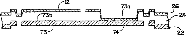
長方形カンチレバーと円形カンチレバーの両方は、その構造が過圧力を受ける場合に、1つの方向に自然の動き止めを有する(特に、ナローギャップ圧力リリーフ経路と、波形しわの溝とバックプレート薄膜との小さな意図的交差)。その他の方向における動き止めを提供するために、パッシベーション窒化物22の島73が、犠牲層としてCMOS金属74を使用して形成される。一方の端部73aがダイヤフラムの端縁に付着させられており、かつ、他方の端部73bが、活性区域の外側のダイヤフラム窒化物の張出しの下に閉じこめられている。図17は、この圧力止め構造を示している。
ギャップの反復性がシリコンマイクロホンにおいて重要である。動作モードの1つは、ダイヤフラムをバックプレートの外側端縁に接触させるように十分に高いバイアス電圧を供給することである。これは非常に反復性の高いギャップを形成し、かつ、優れた感度を与えるのに十分なコンプライアンスが依然として保たれている。
本発明が、本発明の思想またはその中心的特徴から逸脱することなしに、他の特定の形態で具体化されることが可能であることが理解されるだろう。したがって、上記実施形態と具体例とが非限定的な例示のためのものであるとみなされるべきであり、本発明は上記の詳細な説明に限定されるものではない。Technical field
The present invention relates to a small silicon condenser microphone that can be integrated in a CMOS circuit system.
Background prior art
Small silicon condenser microphones that can be integrated into CMOS circuitry require some trade-offs to obtain high sensitivity and low noise in a minimum volume. Typically, a condenser microphone comprises four elements: a fixed perforated backplate, a high compliance movable diaphragm (the backplate and the diaphragm together form two electrodes of a variable air gap capacitor), a voltage bias source, And a buffer amplifier.
The diaphragm must be highly compliant and accurately positioned with respect to the backplate, while the backplate remains stationary and has a minimal airflow through the backplate. It must provide only limited resistance. The realization of all of these features in the form of microphones less than 1 mm in size using integrated circuit materials has heretofore been a difficult task in three aspects. First, silicon-based miniature condenser microphones to date have used diaphragms held by a surrounding frame, with the maximum deflection occurring at the center of the diaphragm. In this configuration, the unremoved stress in the diaphragm material can cause a reduction in diaphragm compliance (if the stress is a tensile stress that stiffens the diaphragm), or Is a compressive stress that causes the diaphragm to buckle), which causes a decrease in positioning accuracy. Typical stress levels in integrated circuit thin films are many times higher than levels at which the diaphragm becomes unusable due to excessive stiffening or buckling if not removed from within the finished diaphragm.
A second problem with diaphragms of size less than 1 mm is that for a given diagram material and thickness, the smaller the size of the diaphragm, the more the compliance tends to drop very sharply. is there. When the unit of the diaphragm compliance is a linear deflection per unit pressure, the compliance is regarded as the fourth power of the diaphragm size. As a specific example, if the material, thickness and shape of the diaphragm are kept the same, reducing the diaphragm diameter by half is presumed to reduce the diagram compliance to 1/16 of its previous value. You.
A third problem in miniaturizing microphones less than 1 mm in size is to maintain a small degree of mechanical damping against diaphragm displacement. In order to keep the capacitor capacitance within a range that can effectively drive the input of the buffer amplifier, the air gap must be reduced as the structure is reduced (the size of the device is small). Approximated as the reciprocal of the square). Unfortunately, the smaller the air gap, the more the damping effect due to the viscous flow of air trapped between the diaphragm and the back plate changes as the inverse of the cube of the size of the air gap. And increase rapidly. The net result is that mechanical damping tends to increase very rapidly, in the form of the inverse of the sixth power of the device size. This attenuation adversely affects the frequency response and, according to established theories, causes pressure fluctuations in the microphone structure that contribute to noise in the microphone output.
Various solutions have been proposed in the past to avoid the problem of overstress in the diaphragm of a small condenser microphone. Such solutions can be categorized according to whether the solution focuses on the diagram material or on the diaphragm structure. In terms of materials, Bergquist and Rudolf's Transducers 91, Proceedings of the International Conference on Solid-State Sensors and Actuators (IEEE, New York, 1991), pp. 266-269, are similar diaphragms made of single crystal silicon. Single crystal silicon is disclosed as a diaphragm material to minimize the occurrence of stress differences with respect to the support.
U.S. Pat.No. 4,571,661 to Hoshino discloses a semiconductor vibration detection device including a semiconductor base and a movable lever having one end secured to the semiconductor base and a free end capable of vibration. . However, Hoshino fails to disclose or suggest a thin film cantilever structure that is responsive to fluid conducted sound pressure and extends over a portion of the opening in the support structure.
U.S. Pat. No. 5,146,453 to Bernstein discloses an all-silicon structure consisting of a single-crystal silicon diaphragm supported around it by a patterned silicon spring.
In terms of diaphragm construction, U.S. Pat.No. 5,490,220 to Loeppert discloses a free plate diaphragm construction wherein the diaphragm is separated from its frame and held only by a set of lateral restraints. ing. According to Loeppert, despite the material mismatch between the diaphragm and its frame, the material stress is completely eliminated in the finished diaphragm.
PCT publication WO 95/34917 discloses a piezoelectric cantilever pressure transducer. Alternatively, the transducer can be a magnetostrictive transducer, a piezoresistive transducer, or a thermal transducer.
However, none of the above solutions can solve this particular thin film stress problem while maintaining good performance in the manufacturing process.
The present invention enables these and other problems to be solved.
Summary of the Invention
It is an object of the present invention to provide a different diaphragm / backplate structure in which the diaphragm shape is based on a cantilever and another backplate ventilation structure suitable for microphones of less than 1 mm is used. To provide. Such microphones can be used for ultrasound, audio, and voice conversion applications.
In the cantilever configuration, the stress of the diaphragm material is relieved in the final diaphragm structure to about the same extent as in the free plate structure, without the need for holding restraints associated with the free plate. In addition, the compliance of the cantilever structure is more than a hundred times greater than the compliance of an edge clamping diaphragm of the same material, span and thickness, which is the above problem due to compliance in diaphragms less than 1 mm in size. Regardless, it facilitates the design of smaller devices.
The diaphragm can be formed on a single silicon wafer with a backplate, integrated CMOS circuitry for backplate voltage bias, and a buffer amplifier. Some embodiments are described below. The method of venting the condenser air gap to minimize mechanical damping is determined on a case-by-case basis in the individual embodiment and is therefore provided on a case-by-case basis in each individual case. The end result is a solution that offers advantages in microphone size and sensitivity, which will be readily apparent to those skilled in the art.
Other features and advantages of the present invention will become apparent from the following detailed description, which proceeds with reference to the accompanying drawings.
[Brief description of the drawings]
FIG. 1 is a perspective view of a first embodiment of a silicon condenser microphone made according to the present invention.
FIG. 1a is a perspective view of a second embodiment of a silicon condenser microphone made in accordance with the present invention.
2 to 9 are cross-sectional views showing successive stages of the manufacture of the microphone of FIG.
6a, 6b, 7a, 8a, 9a, 9b are cross-sectional views showing successive stages of the manufacture of the microphone of FIG. 1a.
FIG. 10 is a perspective view of a third embodiment of a silicon condenser microphone made according to the present invention.
11 and 12 are cross-sectional views showing successive stages of the production of the microphone of FIG.
FIG. 13 is a perspective view of a fourth embodiment of a silicon condenser microphone made according to the present invention.
FIG. 13a is a plan view of the microphone of FIG. 13, with the diaphragm omitted.
13b and 13c are cross-sectional views of the microphone of FIG. 13a.
FIG. 13d is a plan view of the microphone of FIG. 13a, including a diaphragm.
FIGS. 14 and 15 are cross-sectional views showing successive stages of the production of the microphone of FIG.
FIG. 16 is a plan view of a web structure according to a modification of the fourth embodiment of the present invention.
FIG. 16a is a plan view of a modification of the fourth embodiment of the present invention.
16b and 16c are cross-sectional views of the microphone of FIG. 16a.
FIG. 17a is a plan view of an overpressure prevention structure for use with the microphone of the fourth embodiment.
FIG. 17b is a cross-sectional view of the overpressure prevention structure of FIG. 17a.
Detailed description
The present invention may be embodied in various forms of embodiments, and preferred embodiments of the present invention are shown in the accompanying screens and described in detail in the following description. Understand that the content is to be regarded as illustrative of the principles of the invention and that it is not intended to limit the broad aspects of the invention to the embodiments set forth herein. I want to be.
A cantilever design for a
Referring to FIG. 2, as shown in this figure, the present invention preferably is a double-side polished silicon wafer during CMOS processing of other components (not shown) on
Referring to FIG. 3, a low
Similarly, a CMOS process typically leaves a silicon
The
Referring to FIG. 6, as shown in this figure, a
Referring to FIG. 7, as shown therein, a silicon
Referring to FIG. 8, as shown in this figure, a metal layer, preferably chromium, having a thickness of about 0.02 microns, is deposited on the silicon
A thickness of 0.02 microns is used to provide an appropriate balance between stress considerations and conductance considerations. For thinner layers, lower conductance will be obtained, but will give worse results with respect to stress.
Although not explicitly shown, a titanium / tungsten alloy layer, followed by a gold layer, is deposited and patterned to protect the aluminum bond pads on the
The final micromachining stage is shown in FIG. At this stage, the entire wafer is etched with an anisotropic etchant, preferably potassium hydroxide (KOH). This step forms a
The cantilevered
In order to adapt the diaphragm compliance to the intended pressure range, and to reduce the tendency of the
A structure has a "bending moment" that relates its shape to its stiffness. The film increases the bending moment as its thickness increases, but at the same time increases the diaphragm mass unnecessarily, and simply increases the forces and moments that promote the tendency to curl. Both types of structures described below perform their function by increasing the bending moment of the diaphragm without changing the film thickness.
A first structure for increasing the bending moment is to wrinkle a diaphragm formed of a single thin film layer. The first approach would consist of corrugating the cantilever from root to tip. However, in the thin film layer, the tendency to curl along the cantilever is equal to the tendency to curl in the transverse direction of the cantilever, so a structure having only vertical linear wrinkles is still curl in the transverse direction. there's a possibility that. For this, a higher performance wrinkle pattern must be used which increases the bending moment in every cross section of the diaphragm. One such wrinkle pattern is shown in FIG. 1a. Various other patterns can be used. As shown in FIG. 1a, no matter what cross section is taken, every cross section will traverse multiple corrugations.
The manufacture of the diaphragm of FIG. 1a is similar to the manufacture of the diaphragm of FIG. 1 except for the steps shown in FIGS. 6a, 6b, 7a, 8a, 9a and 9b.
Referring to FIG. 6a, as shown in this figure, the
As shown in FIG. 6b, a second
Referring to FIG. 7a, a silicon
Referring to FIG. 8a, a metal layer, preferably about 0.01 microns thick, of chromium is deposited and patterned on the silicon
Although not shown in detail, as in the first embodiment, a titanium / tungsten alloy layer followed by a gold layer is deposited to protect the aluminum bonding pads elsewhere on the
The final micromachining stage is shown in FIG. 9a. At this stage, the
If deeper wrinkles are required, the silicon is trench etched prior to sacrificial layer deposition and patterning to increase the overall amplitude of the wrinkles.
The low frequency roll-off point of the microphone is determined by the reciprocal of the product of the back volume compliance (in acoustic farads) and the acoustic resistance (in acoustic ohms) of the pressure equalization path. The acoustic equalization path of this device is around the edge of the cantilever diaphragm and continues into a hole in the silicon substrate. For very small microphones with a back volume of 2 to 3 cubic millimeters, as sought in the present invention, the acoustic resistance of this path is very high to maintain a flat response below 100 Hz. Must be high and about one million acoustic ohms.
FIG. 9b is a cross-sectional view of FIG. 1a, taken along line 9b-9b of FIG. 1a. As shown in FIG. 9b, high acoustic resistance is obtained by forming an overlapping
The various vertical dimensions required for the
For all condenser microphones, there is a combination of acoustic level and bias voltage that results in irreversible collapse of the diaphragm on its backplate. The position of the diaphragm under the condition of zero bias voltage / zero sound pressure is called the no-load position of the diaphragm. In typical applications, the bias voltage is adjustable, but it is often difficult to control the maximum sound pressure. This irreversible collapse can be prevented if the movement of the diaphragm from the no-load position is limited and the proper bias voltage is maintained.
In the microphone of the present invention, the small height "h" (see FIG. 9b) of the
In the above structure, most of the area under the
A second structure for increasing the bending moment is to form the
The manufacturing method of this diaphragm is similar to the manufacturing method disclosed above with respect to the embodiment of FIG. 1a, but is shown in more detail in FIGS.
In this method, after the deposition and patterning of a first
Another preferred diaphragm structure is shown in FIG. This structure includes a circular diaphragm fixed at its center. An advantage of this shape is that it eliminates the need for the two free side edges of a straight cantilever, where suppression of lateral curl is most difficult. The only free edge left is the circular perimeter. For a given diaphragm size, diaphragm material and diaphragm thickness, if the structure is kept uniform within dimensions equal to the amplitude of the wrinkles, the compliance of the structure will depend on the edge support diaphragm. It is halfway between compliance and linear cantilever compliance, five times the former and about one-twentieth of the latter. The curling tendency of this structure is also intermediate. Furthermore, the compliance of this structure can be adjusted to the required value by incorporating waveform wrinkles of appropriate amplitude. Such wrinkles can be radial, circular (which is the preferred shape), or tangential to the inner radius, such as a toy windmill. In the case of circular wrinkles, circular wrinkles are preferred because they can be formed without interruption by the diaphragm fixing area.
The process of manufacturing the embodiment of FIG. 13 is similar to the process of manufacturing the embodiment of FIG. 1a, except for the step of forming the
The fixing
The preferred method described above is such that a stretched perforated membrane structure or
In this center supported circular diaphragm design, compliance in the electrostatic region is the result of the sum of the compliance of the
For greater compliance, the
The advantage of a silicon center support for a circular diaphragm is that this support is a very flat and stable base for the diaphragm. The central silicon support is also more isolated from package generated stresses than the tensile thin film support structure. Further, since the support is made of bulk silicon, the unremoved thin film stress at the diaphragm attachment is negligible compared to the tensile thin film support structure.
This preferred method of substrate etching (anisotropic etching) can create square holes. The perimeter of the circular diaphragm must either overlap a majority of the surrounding substrate surface or leave corners of the substrate hole that do not overlap, based on the relative size selected for the diaphragm and the substrate hole. In the former case, the bulk of the air is trapped between the diaphragm and the substrate, requiring perforation of the diaphragm as described above to avoid viscous damping due to the flow of air being moved. In the latter case, large leakage areas are created at the corners of the substrate hole, but the toughened thin film (preferably a silicon nitride passivation layer) used in connection with the diaphragm support method is used. If it is stretched to fill the inside of the corner, the leakage area can be eliminated. Thus, the area of the narrow gap overlap between the diaphragm and the substrate is reformed as needed to suppress leakage through the pneumatic relief path. The free end of the taut film added into the corner of the hole tends to curl somewhat, which reduces the effectiveness of controlling the narrow gap in the pneumatic relief path. In the preferred design described above, several additional taut thin film strips 62a are included that flatten the free edge of the corner thin film area by pulling the free edge toward the center of the device.
A capacitor is incorporated in the device at a location near the edge of the diaphragm, since the maximum amplitude of the pressure-induced vibration occurs at that location. Diaphragm electrodes are formed by metallizing the capacitor area of the diaphragm. The structure of the backplate depends on the size chosen for the diaphragm. In the case of a large diaphragm overlying the solid substrate surface surrounding the perimeter of the substrate hole, the backplate electrode is formed by metallizing the surface of the passivation coated substrate.
In the case of a smaller diaphragm, as shown in FIG.13d, which pulls the corners of the substrate hole as described above and the area of the thin film must already fill the area of the taut thin film, it is even simpler. The backplate is formed by stretching to form a freestanding backplate thin film structure located below the metallized perimeter area of the diaphragm. Thereafter, these additional taut thin film sections are also metallized to form the
Electrical connection to the metallized
A problem that arises when certain diaphragm wrinkle shapes are combined with the backplate perforation pattern is that some low areas of the wrinkle pattern hang down on the backplate thin film material. This creates an area in which the air gap is about 1 micrometer, while the air gap is 4 micrometers elsewhere. As noted above, the viscous damping effect is approximated as the inverse of the cube of the air gap, so mechanical damping can accumulate more than 50 times faster per unit area in these locations than elsewhere in the structure. I do.
Two ways to avoid this are included herein. The first method is to pierce the diaphragm at such a location, as described above. If these locations are not too many, the diaphragm wrinkles are not upset enough to significantly change the compliance or curl suppression of the diaphragm.
A second way to avoid this damping effect is to remove all wrinkle / backplate intersections. FIGS. 16, 16a, 16b, and 16c illustrate such a design. This approach uses a generally radial arrangement of corrugations and a corresponding radial arrangement of
Both rectangular and circular cantilevers have a natural detent in one direction if the structure is over-pressed (especially narrow gap pressure relief paths, small wrinkling grooves and backplate membranes). Intentional intersection). To provide detent in other directions,
Gap repeatability is important in silicon microphones. One mode of operation is to provide a sufficiently high bias voltage to bring the diaphragm into contact with the outer edge of the backplate. This creates a very repeatable gap and still maintains sufficient compliance to provide excellent sensitivity.
It will be understood that the present invention can be embodied in other specific forms without departing from the spirit of the invention or its central features. Therefore, the above embodiments and specific examples should be considered as non-limiting examples, and the present invention is not limited to the above detailed description.
Claims (16)
支持構造(11)を形成し且つ開口(30)を有する半導体基板(16)と、
前記開口の一部分の上に延びている流体伝導音圧に応答するダイヤフラム(12)を形成しており、基部端部(12a)と末端端部(12b)とを有し、前記基部端部が前記支持構造に取り付けられ、かつ、前記末端端部が前記支持構造から分離されかつ前記支持構造の一部分の上に延びている薄膜カンチレバー構造と、
可動電極(14a)と固定電極(14b)とを有し、前記可動電極が前記構造の前記末端端部の上に配置され、前記固定電極が前記可動電極に近接して前記支持構造の上に配置され、かつ、前記コンデンサマイクロホンが前記固定電極に対する前記可動電極の位置に比例した出力を生じさせる可変ギャップコンデンサ(14)
とを含むソリッドステートコンデンサマイクロホン。A solid state condenser microphone,
A semiconductor substrate (16) forming a support structure (11) and having an opening (30);
Forming a diaphragm (12) responsive to fluid conducted sound pressure extending over a portion of the opening, the diaphragm (12) having a base end (12a) and a distal end (12b), wherein the base end is A thin-film cantilever structure attached to the support structure and having the distal end separated from the support structure and extending over a portion of the support structure;
A movable electrode (14a) and a fixed electrode (14b), wherein the movable electrode is disposed on the distal end of the structure, and the fixed electrode is disposed on the support structure in proximity to the movable electrode. A variable gap capacitor (14) disposed and wherein the condenser microphone produces an output proportional to the position of the movable electrode relative to the fixed electrode (14)
And including a solid state condenser microphone.
Applications Claiming Priority (3)
| Application Number | Priority Date | Filing Date | Title |
|---|---|---|---|
| US08/805,983 | 1997-02-25 | ||
| US08/805,983 US5870482A (en) | 1997-02-25 | 1997-02-25 | Miniature silicon condenser microphone |
| PCT/US1998/003144 WO1998037388A1 (en) | 1997-02-25 | 1998-02-19 | Miniature silicon condenser microphone |
Publications (2)
| Publication Number | Publication Date |
|---|---|
| JP2001518246A JP2001518246A (en) | 2001-10-09 |
| JP3556676B2 true JP3556676B2 (en) | 2004-08-18 |
Family
ID=25193025
Family Applications (1)
| Application Number | Title | Priority Date | Filing Date |
|---|---|---|---|
| JP53684198A Expired - Fee Related JP3556676B2 (en) | 1997-02-25 | 1998-02-19 | Small silicon condenser microphone |
Country Status (8)
| Country | Link |
|---|---|
| US (1) | US5870482A (en) |
| EP (1) | EP1012547B1 (en) |
| JP (1) | JP3556676B2 (en) |
| AT (1) | ATE266190T1 (en) |
| AU (1) | AU6658798A (en) |
| DE (1) | DE69823679T2 (en) |
| DK (1) | DK1012547T3 (en) |
| WO (1) | WO1998037388A1 (en) |
Families Citing this family (209)
| Publication number | Priority date | Publication date | Assignee | Title |
|---|---|---|---|---|
| US6248249B1 (en) * | 1997-07-15 | 2001-06-19 | Silverbrook Research Pty Ltd. | Method of manufacture of a Lorenz diaphragm electromagnetic ink jet printer |
| EP1093685A4 (en) * | 1998-06-05 | 2004-09-01 | Knowles Electronics Llc | Solid-state receiver |
| US6088463A (en) | 1998-10-30 | 2000-07-11 | Microtronic A/S | Solid state silicon-based condenser microphone |
| DE19852878B4 (en) * | 1998-11-16 | 2009-11-12 | Infineon Technologies Ag | Micromechanical device and manufacturing method thereof |
| DE60003199T2 (en) * | 1999-09-06 | 2004-07-01 | Sonionmems A/S | SILICONE BASED SENSOR SYSTEMS |
| US6522762B1 (en) * | 1999-09-07 | 2003-02-18 | Microtronic A/S | Silicon-based sensor system |
| JP3611779B2 (en) | 1999-12-09 | 2005-01-19 | シャープ株式会社 | Electrical signal-acoustic signal converter, method for manufacturing the same, and electrical signal-acoustic converter |
| DE10195878T1 (en) * | 2000-03-07 | 2003-06-12 | Hearworks Pty Ltd | Double condenser microphone |
| US6535460B2 (en) | 2000-08-11 | 2003-03-18 | Knowles Electronics, Llc | Miniature broadband acoustic transducer |
| US6987859B2 (en) | 2001-07-20 | 2006-01-17 | Knowles Electronics, Llc. | Raised microstructure of silicon based device |
| US7434305B2 (en) * | 2000-11-28 | 2008-10-14 | Knowles Electronics, Llc. | Method of manufacturing a microphone |
| US7439616B2 (en) * | 2000-11-28 | 2008-10-21 | Knowles Electronics, Llc | Miniature silicon condenser microphone |
| US7166910B2 (en) * | 2000-11-28 | 2007-01-23 | Knowles Electronics Llc | Miniature silicon condenser microphone |
| US8629005B1 (en) | 2000-11-28 | 2014-01-14 | Knowles Electronics, Llc | Methods of manufacture of bottom port surface mount silicon condenser microphone packages |
| US6741709B2 (en) * | 2000-12-20 | 2004-05-25 | Shure Incorporated | Condenser microphone assembly |
| US6847090B2 (en) | 2001-01-24 | 2005-01-25 | Knowles Electronics, Llc | Silicon capacitive microphone |
| US7103196B2 (en) | 2001-03-12 | 2006-09-05 | Knowles Electronics, Llc. | Method for reducing distortion in a receiver |
| US6896850B2 (en) * | 2001-03-26 | 2005-05-24 | Kumetrix, Inc. | Silicon nitride window for microsampling device and method of construction |
| JP2002345092A (en) * | 2001-05-15 | 2002-11-29 | Citizen Electronics Co Ltd | Manufacturing method for condenser microphone |
| US6859542B2 (en) | 2001-05-31 | 2005-02-22 | Sonion Lyngby A/S | Method of providing a hydrophobic layer and a condenser microphone having such a layer |
| US7023066B2 (en) * | 2001-11-20 | 2006-04-04 | Knowles Electronics, Llc. | Silicon microphone |
| AU2002365352A1 (en) | 2001-11-27 | 2003-06-10 | Corporation For National Research Initiatives | A miniature condenser microphone and fabrication method therefor |
| DE10160830A1 (en) * | 2001-12-11 | 2003-06-26 | Infineon Technologies Ag | Micromechanical sensor comprises a counter element lying opposite a moving membrane over a hollow chamber and containing openings which are formed by slits |
| DE10205585A1 (en) * | 2002-02-11 | 2003-08-28 | Infineon Technologies Ag | Micromechanical component and method for its production |
| FI118505B (en) * | 2002-06-04 | 2007-11-30 | Aspocomp Oy | Acoustically active element formed in a multilayer circuit board structure, a method for forming an acoustically active element in a multilayer circuit board structure, and a multilayer circuit board structure |
| US7072482B2 (en) | 2002-09-06 | 2006-07-04 | Sonion Nederland B.V. | Microphone with improved sound inlet port |
| US6781231B2 (en) * | 2002-09-10 | 2004-08-24 | Knowles Electronics Llc | Microelectromechanical system package with environmental and interference shield |
| US6667189B1 (en) | 2002-09-13 | 2003-12-23 | Institute Of Microelectronics | High performance silicon condenser microphone with perforated single crystal silicon backplate |
| DE10247487A1 (en) * | 2002-10-11 | 2004-05-06 | Infineon Technologies Ag | Membrane and process for its manufacture |
| US7142682B2 (en) * | 2002-12-20 | 2006-11-28 | Sonion Mems A/S | Silicon-based transducer for use in hearing instruments and listening devices |
| US7049051B2 (en) * | 2003-01-23 | 2006-05-23 | Akustica, Inc. | Process for forming and acoustically connecting structures on a substrate |
| US7501703B2 (en) * | 2003-02-28 | 2009-03-10 | Knowles Electronics, Llc | Acoustic transducer module |
| US7382048B2 (en) * | 2003-02-28 | 2008-06-03 | Knowles Electronics, Llc | Acoustic transducer module |
| JP2004356708A (en) * | 2003-05-27 | 2004-12-16 | Hosiden Corp | Sound detection mechanism and manufacturing method thereof |
| US7876924B1 (en) | 2003-10-20 | 2011-01-25 | The Research Foundation Of State University Of New York | Robust diaphragm for an acoustic device |
| US8582795B2 (en) * | 2003-10-20 | 2013-11-12 | The Research Foundation Of State University Of New York | Robust diaphragm for an acoustic device |
| US20050095814A1 (en) * | 2003-11-05 | 2005-05-05 | Xu Zhu | Ultrathin form factor MEMS microphones and microspeakers |
| US7165647B2 (en) * | 2003-12-18 | 2007-01-23 | Pei-Chau Lee | Mechanical acoustic filter by erosion etching |
| US7495302B2 (en) * | 2004-03-03 | 2009-02-24 | Robert Bosch Gmbh | Micromechanical component having a diaphragm |
| JP4137158B2 (en) * | 2004-03-05 | 2008-08-20 | 松下電器産業株式会社 | Electret condenser microphone |
| EP1599067B1 (en) | 2004-05-21 | 2013-05-01 | Epcos Pte Ltd | Detection and control of diaphragm collapse in condenser microphones |
| DK1638366T3 (en) * | 2004-09-20 | 2015-12-14 | Sonion Nederland Bv | microphone device |
| TWI260938B (en) * | 2004-10-01 | 2006-08-21 | Ind Tech Res Inst | Dynamic pressure sensing structure |
| US7346178B2 (en) * | 2004-10-29 | 2008-03-18 | Silicon Matrix Pte. Ltd. | Backplateless silicon microphone |
| JP4539450B2 (en) * | 2004-11-04 | 2010-09-08 | オムロン株式会社 | Capacitive vibration sensor and manufacturing method thereof |
| US7936894B2 (en) * | 2004-12-23 | 2011-05-03 | Motorola Mobility, Inc. | Multielement microphone |
| US7795695B2 (en) | 2005-01-27 | 2010-09-14 | Analog Devices, Inc. | Integrated microphone |
| DE102005008514B4 (en) * | 2005-02-24 | 2019-05-16 | Tdk Corporation | Microphone membrane and microphone with the microphone membrane |
| DE102005008512B4 (en) | 2005-02-24 | 2016-06-23 | Epcos Ag | Electrical module with a MEMS microphone |
| DE102005008511B4 (en) * | 2005-02-24 | 2019-09-12 | Tdk Corporation | MEMS microphone |
| JP4715260B2 (en) * | 2005-03-23 | 2011-07-06 | ヤマハ株式会社 | Condenser microphone and manufacturing method thereof |
| US20070071268A1 (en) * | 2005-08-16 | 2007-03-29 | Analog Devices, Inc. | Packaged microphone with electrically coupled lid |
| US7825484B2 (en) * | 2005-04-25 | 2010-11-02 | Analog Devices, Inc. | Micromachined microphone and multisensor and method for producing same |
| US7449356B2 (en) * | 2005-04-25 | 2008-11-11 | Analog Devices, Inc. | Process of forming a microphone using support member |
| US7885423B2 (en) | 2005-04-25 | 2011-02-08 | Analog Devices, Inc. | Support apparatus for microphone diaphragm |
| JP2007013509A (en) * | 2005-06-30 | 2007-01-18 | Sanyo Electric Co Ltd | Acoustic sensor and diaphragm |
| JP2007043327A (en) * | 2005-08-01 | 2007-02-15 | Star Micronics Co Ltd | Condenser microphone |
| US20070040231A1 (en) * | 2005-08-16 | 2007-02-22 | Harney Kieran P | Partially etched leadframe packages having different top and bottom topologies |
| US8477983B2 (en) * | 2005-08-23 | 2013-07-02 | Analog Devices, Inc. | Multi-microphone system |
| US8130979B2 (en) * | 2005-08-23 | 2012-03-06 | Analog Devices, Inc. | Noise mitigating microphone system and method |
| US7961897B2 (en) * | 2005-08-23 | 2011-06-14 | Analog Devices, Inc. | Microphone with irregular diaphragm |
| US8351632B2 (en) * | 2005-08-23 | 2013-01-08 | Analog Devices, Inc. | Noise mitigating microphone system and method |
| SG131039A1 (en) * | 2005-09-14 | 2007-04-26 | Bse Co Ltd | Condenser microphone and packaging method for the same |
| CN1933682B (en) * | 2005-09-14 | 2010-08-18 | 佳乐电子股份有限公司 | Vibrating diaphragm chip of silicon microphone and producing method thereof |
| DE102005053765B4 (en) * | 2005-11-10 | 2016-04-14 | Epcos Ag | MEMS package and method of manufacture |
| DE102005053767B4 (en) * | 2005-11-10 | 2014-10-30 | Epcos Ag | MEMS microphone, method of manufacture and method of installation |
| US20090116675A1 (en) * | 2005-12-14 | 2009-05-07 | Yuichi Miyoshi | Mems diaphragm structure and method for forming the same |
| CN105704622A (en) * | 2006-01-20 | 2016-06-22 | 应美盛股份有限公司 | Support Apparatus for Microphone Diaphragm |
| TW200738028A (en) | 2006-02-24 | 2007-10-01 | Yamaha Corp | Condenser microphone |
| JP4605470B2 (en) * | 2006-03-31 | 2011-01-05 | ヤマハ株式会社 | Condenser microphone |
| JP4737720B2 (en) * | 2006-03-06 | 2011-08-03 | ヤマハ株式会社 | Diaphragm, manufacturing method thereof, condenser microphone having the diaphragm, and manufacturing method thereof |
| JP2007228345A (en) * | 2006-02-24 | 2007-09-06 | Yamaha Corp | Capacitor microphone |
| JP2007295308A (en) * | 2006-04-25 | 2007-11-08 | Citizen Electronics Co Ltd | Method of manufacturing electret capaciter microphone |
| US7493823B2 (en) * | 2006-06-16 | 2009-02-24 | Honeywell International Inc. | Pressure transducer with differential amplifier |
| US8081783B2 (en) * | 2006-06-20 | 2011-12-20 | Industrial Technology Research Institute | Miniature acoustic transducer |
| JP4797829B2 (en) * | 2006-06-26 | 2011-10-19 | ヤマハ株式会社 | Condenser microphone and method of manufacturing condenser microphone |
| US8344487B2 (en) * | 2006-06-29 | 2013-01-01 | Analog Devices, Inc. | Stress mitigation in packaged microchips |
| US20080019543A1 (en) * | 2006-07-19 | 2008-01-24 | Yamaha Corporation | Silicon microphone and manufacturing method therefor |
| EP2044802B1 (en) * | 2006-07-25 | 2013-03-27 | Analog Devices, Inc. | Multiple microphone system |
| US20080042223A1 (en) * | 2006-08-17 | 2008-02-21 | Lu-Lee Liao | Microelectromechanical system package and method for making the same |
| US20080075308A1 (en) * | 2006-08-30 | 2008-03-27 | Wen-Chieh Wei | Silicon condenser microphone |
| US20080083957A1 (en) * | 2006-10-05 | 2008-04-10 | Wen-Chieh Wei | Micro-electromechanical system package |
| US7894622B2 (en) | 2006-10-13 | 2011-02-22 | Merry Electronics Co., Ltd. | Microphone |
| US8165323B2 (en) | 2006-11-28 | 2012-04-24 | Zhou Tiansheng | Monolithic capacitive transducer |
| TW200847827A (en) * | 2006-11-30 | 2008-12-01 | Analog Devices Inc | Microphone system with silicon microphone secured to package lid |
| EP1931173B1 (en) | 2006-12-06 | 2011-07-20 | Electronics and Telecommunications Research Institute | Condenser microphone having flexure hinge diaphragm and method of manufacturing the same |
| US8121315B2 (en) * | 2007-03-21 | 2012-02-21 | Goer Tek Inc. | Condenser microphone chip |
| CN101321408B (en) * | 2007-06-06 | 2012-12-12 | 歌尔声学股份有限公司 | Internal rotation beam diaphragm and microphone chip composed by the same |
| US20080247573A1 (en) * | 2007-04-06 | 2008-10-09 | Novusonic Corporation | Miniature capacitive acoustic sensor with stress-relieved actively clamped diaphragm |
| US8705775B2 (en) * | 2007-04-25 | 2014-04-22 | University Of Florida Research Foundation, Inc. | Capacitive microphone with integrated cavity |
| US8103027B2 (en) * | 2007-06-06 | 2012-01-24 | Analog Devices, Inc. | Microphone with reduced parasitic capacitance |
| US9078068B2 (en) * | 2007-06-06 | 2015-07-07 | Invensense, Inc. | Microphone with aligned apertures |
| CN101321407B (en) * | 2007-06-06 | 2012-12-26 | 歌尔声学股份有限公司 | Girder-type diaphragm and microphone chip composed by the same |
| US7694610B2 (en) * | 2007-06-27 | 2010-04-13 | Siemens Medical Solutions Usa, Inc. | Photo-multiplier tube removal tool |
| GB2451909B (en) * | 2007-08-17 | 2012-07-11 | Wolfson Microelectronics Plc | Mems process and device |
| US8723279B2 (en) * | 2007-07-24 | 2014-05-13 | Rohm Co., Ltd. | MEMS sensor, and MEMS sensor manufacturing method |
| JP5412031B2 (en) | 2007-07-24 | 2014-02-12 | ローム株式会社 | MEMS sensor |
| JP2009028808A (en) | 2007-07-24 | 2009-02-12 | Rohm Co Ltd | Mems sensor and manufacturing method of mems sensor |
| JP2009028807A (en) | 2007-07-24 | 2009-02-12 | Rohm Co Ltd | Mems sensor |
| US8208671B2 (en) * | 2008-01-16 | 2012-06-26 | Analog Devices, Inc. | Microphone with backside cavity that impedes bubble formation |
| US8144906B2 (en) * | 2008-05-21 | 2012-03-27 | Akustica, Inc. | Wind immune microphone |
| US20110138902A1 (en) * | 2008-05-27 | 2011-06-16 | Tufts University | Mems microphone array on a chip |
| JP5374077B2 (en) | 2008-06-16 | 2013-12-25 | ローム株式会社 | MEMS sensor |
| US7951636B2 (en) * | 2008-09-22 | 2011-05-31 | Solid State System Co. Ltd. | Method for fabricating micro-electro-mechanical system (MEMS) device |
| JP2010098518A (en) * | 2008-10-16 | 2010-04-30 | Rohm Co Ltd | Method of manufacturing mems sensor, and mems sensor |
| TWI374514B (en) | 2008-12-12 | 2012-10-11 | Ind Tech Res Inst | Truss structure and manufacturing method thereof |
| EP2239961A1 (en) * | 2009-04-06 | 2010-10-13 | Nxp B.V. | Backplate for microphone |
| WO2010139050A1 (en) | 2009-06-01 | 2010-12-09 | Tiansheng Zhou | Mems micromirror and micromirror array |
| EP2271134A1 (en) | 2009-07-02 | 2011-01-05 | Nxp B.V. | Proximity sensor comprising an acoustic transducer for receiving sound signals in the human audible range and for emitting and receiving ultrasonic signals. |
| EP2271129A1 (en) * | 2009-07-02 | 2011-01-05 | Nxp B.V. | Transducer with resonant cavity |
| EP2269746B1 (en) | 2009-07-02 | 2014-05-14 | Nxp B.V. | Collapsed mode capacitive sensor |
| JPWO2011039798A1 (en) * | 2009-09-29 | 2013-02-21 | パイオニア株式会社 | MEMS sensor and sensor array including the same |
| WO2011059868A1 (en) * | 2009-11-16 | 2011-05-19 | Analog Devices, Inc. | Microphone with backplate having specially shaped through-holes |
| JP2011114506A (en) * | 2009-11-26 | 2011-06-09 | Funai Electric Co Ltd | Microphone unit |
| US8577063B2 (en) * | 2010-02-18 | 2013-11-05 | Analog Devices, Inc. | Packages and methods for packaging MEMS microphone devices |
| US8656772B2 (en) | 2010-03-22 | 2014-02-25 | Honeywell International Inc. | Flow sensor with pressure output signal |
| JP5206726B2 (en) | 2010-04-12 | 2013-06-12 | 株式会社デンソー | Mechanical quantity detection device and manufacturing method thereof |
| CN101883306B (en) * | 2010-04-27 | 2012-12-12 | 瑞声声学科技(深圳)有限公司 | Diaphragm and capacitance microphone comprising diaphragm |
| DE102011050040B4 (en) | 2010-05-14 | 2016-10-06 | National Tsing Hua University | Capacitive microsystem microphone |
| WO2011146846A2 (en) * | 2010-05-21 | 2011-11-24 | Sand9, Inc. | Micromechanical membranes and related structures and methods |
| CN102264020B (en) * | 2010-05-26 | 2013-12-25 | 国立清华大学 | Micro-Electro-Mechanical condenser microphone |
| JP5588745B2 (en) * | 2010-05-27 | 2014-09-10 | オムロン株式会社 | Acoustic transducer and microphone using the acoustic transducer |
| US8436435B2 (en) | 2010-07-27 | 2013-05-07 | National Tsing Hua University | MEMS capacitive microphone |
| US8464589B2 (en) * | 2010-10-14 | 2013-06-18 | Solid State System Co., Ltd. | Micro-electromechanical systems (MEMS) structure |
| US10551613B2 (en) | 2010-10-20 | 2020-02-04 | Tiansheng ZHOU | Micro-electro-mechanical systems micromirrors and micromirror arrays |
| US9036231B2 (en) | 2010-10-20 | 2015-05-19 | Tiansheng ZHOU | Micro-electro-mechanical systems micromirrors and micromirror arrays |
| US8616065B2 (en) | 2010-11-24 | 2013-12-31 | Honeywell International Inc. | Pressure sensor |
| US8695417B2 (en) | 2011-01-31 | 2014-04-15 | Honeywell International Inc. | Flow sensor with enhanced flow range capability |
| CN103493510B (en) | 2011-02-15 | 2016-09-14 | 富士胶卷迪马蒂克斯股份有限公司 | Use the piezoelectric transducer of micro-dome array |
| US9167354B2 (en) * | 2011-03-09 | 2015-10-20 | Sennheiser Electronic Gmbh & Co. Kg | Electroacoustic sound transducer |
| US8447057B2 (en) | 2011-03-18 | 2013-05-21 | Analog Devices, Inc. | Packages and methods for packaging MEMS microphone devices |
| US8625832B2 (en) | 2011-04-04 | 2014-01-07 | Invensense, Inc. | Packages and methods for packaging microphone devices |
| US8450213B2 (en) | 2011-04-13 | 2013-05-28 | Fujifilm Corporation | Forming a membrane having curved features |
| US8503699B2 (en) | 2011-06-01 | 2013-08-06 | Infineon Technologies Ag | Plate, transducer and methods for making and operating a transducer |
| US8969980B2 (en) * | 2011-09-23 | 2015-03-03 | Knowles Electronics, Llc | Vented MEMS apparatus and method of manufacture |
| US9031266B2 (en) * | 2011-10-11 | 2015-05-12 | Infineon Technologies Ag | Electrostatic loudspeaker with membrane performing out-of-plane displacement |
| US9374643B2 (en) | 2011-11-04 | 2016-06-21 | Knowles Electronics, Llc | Embedded dielectric as a barrier in an acoustic device and method of manufacture |
| US9078069B2 (en) | 2012-01-11 | 2015-07-07 | Invensense, Inc. | MEMS microphone with springs and interior support |
| US9385634B2 (en) | 2012-01-26 | 2016-07-05 | Tiansheng ZHOU | Rotational type of MEMS electrostatic actuator |
| US8779535B2 (en) | 2012-03-14 | 2014-07-15 | Analog Devices, Inc. | Packaged integrated device die between an external and internal housing |
| US9409763B2 (en) * | 2012-04-04 | 2016-08-09 | Infineon Technologies Ag | MEMS device and method of making a MEMS device |
| CN202617341U (en) * | 2012-05-04 | 2012-12-19 | 瑞声声学科技(常州)有限公司 | Flat sounder |
| US9003897B2 (en) | 2012-05-10 | 2015-04-14 | Honeywell International Inc. | Temperature compensated force sensor |
| US9491539B2 (en) | 2012-08-01 | 2016-11-08 | Knowles Electronics, Llc | MEMS apparatus disposed on assembly lid |
| US9078063B2 (en) | 2012-08-10 | 2015-07-07 | Knowles Electronics, Llc | Microphone assembly with barrier to prevent contaminant infiltration |
| US8987842B2 (en) * | 2012-09-14 | 2015-03-24 | Solid State System Co., Ltd. | Microelectromechanical system (MEMS) device and fabrication method thereof |
| GB2506174A (en) * | 2012-09-24 | 2014-03-26 | Wolfson Microelectronics Plc | Protecting a MEMS device from excess pressure and shock |
| US9181086B1 (en) | 2012-10-01 | 2015-11-10 | The Research Foundation For The State University Of New York | Hinged MEMS diaphragm and method of manufacture therof |
| US9156680B2 (en) | 2012-10-26 | 2015-10-13 | Analog Devices, Inc. | Packages and methods for packaging |
| US9052217B2 (en) | 2012-11-09 | 2015-06-09 | Honeywell International Inc. | Variable scale sensor |
| US8921956B2 (en) | 2013-01-25 | 2014-12-30 | Infineon Technologies Ag | MEMS device having a back plate with elongated protrusions |
| US9676614B2 (en) | 2013-02-01 | 2017-06-13 | Analog Devices, Inc. | MEMS device with stress relief structures |
| US20140247954A1 (en) | 2013-03-01 | 2014-09-04 | Silicon Audio, Inc. | Entrained Microphones |
| US9082883B2 (en) | 2013-03-04 | 2015-07-14 | Unisem (M) Berhad | Top port MEMS cavity package and method of manufacture thereof |
| US8999757B2 (en) | 2013-03-04 | 2015-04-07 | Unisem (M) Berhad | Top port MEMS cavity package and method of manufacture thereof |
| WO2014194316A1 (en) | 2013-05-31 | 2014-12-04 | Robert Bosch Gmbh | Trapped membrane |
| DE102013106353B4 (en) * | 2013-06-18 | 2018-06-28 | Tdk Corporation | Method for applying a structured coating to a component |
| GB2515836B (en) * | 2013-07-05 | 2016-01-20 | Cirrus Logic Int Semiconductor Ltd | MEMS device and process |
| DE102013213717A1 (en) * | 2013-07-12 | 2015-01-15 | Robert Bosch Gmbh | MEMS device with a microphone structure and method for its manufacture |
| DE102013223359A1 (en) * | 2013-11-15 | 2015-05-21 | Robert Bosch Gmbh | Printed circuit board for the 2nd level mounting of a microphone component and microphone module with such a printed circuit board |
| DE102013224718A1 (en) * | 2013-12-03 | 2015-06-03 | Robert Bosch Gmbh | MEMS microphone component and device having such a MEMS microphone component |
| DE102014203881A1 (en) | 2014-03-04 | 2015-09-10 | Robert Bosch Gmbh | Component with microphone and media sensor function |
| JP6364653B2 (en) | 2014-05-20 | 2018-08-01 | Tdk株式会社 | Microphone and method of operating the microphone |
| DE102014108984B4 (en) | 2014-06-26 | 2017-04-06 | Tdk Corporation | transducer element |
| CN204046818U (en) | 2014-07-28 | 2014-12-24 | 瑞声声学科技(深圳)有限公司 | Capacitance MEMS (micro-electro-mechanical system) microphone |
| US9369804B2 (en) * | 2014-07-28 | 2016-06-14 | Robert Bosch Gmbh | MEMS membrane overtravel stop |
| US10167189B2 (en) | 2014-09-30 | 2019-01-01 | Analog Devices, Inc. | Stress isolation platform for MEMS devices |
| US9743191B2 (en) | 2014-10-13 | 2017-08-22 | Knowles Electronics, Llc | Acoustic apparatus with diaphragm supported at a discrete number of locations |
| US9872116B2 (en) | 2014-11-24 | 2018-01-16 | Knowles Electronics, Llc | Apparatus and method for detecting earphone removal and insertion |
| CN104507014B (en) * | 2014-12-26 | 2018-08-28 | 上海集成电路研发中心有限公司 | A kind of MEMS microphone and its manufacturing method with fold-type vibrating membrane |
| US9554207B2 (en) | 2015-04-30 | 2017-01-24 | Shure Acquisition Holdings, Inc. | Offset cartridge microphones |
| US9565493B2 (en) | 2015-04-30 | 2017-02-07 | Shure Acquisition Holdings, Inc. | Array microphone system and method of assembling the same |
| DE102015107557A1 (en) * | 2015-05-13 | 2016-11-17 | USound GmbH | Circuit board module with a continuous recess and related sound transducer arrangement and manufacturing method |
| US10045126B2 (en) * | 2015-07-07 | 2018-08-07 | Invensense, Inc. | Microelectromechanical microphone having a stationary inner region |
| DE102015213774A1 (en) * | 2015-07-22 | 2017-01-26 | Robert Bosch Gmbh | MEMS component with sound-pressure-sensitive membrane element and piezosensitive signal detection |
| US9794661B2 (en) | 2015-08-07 | 2017-10-17 | Knowles Electronics, Llc | Ingress protection for reducing particle infiltration into acoustic chamber of a MEMS microphone package |
| JP6604626B2 (en) | 2015-08-21 | 2019-11-13 | 国立大学法人東北大学 | Detection device |
| US9401158B1 (en) | 2015-09-14 | 2016-07-26 | Knowles Electronics, Llc | Microphone signal fusion |
| US10131538B2 (en) | 2015-09-14 | 2018-11-20 | Analog Devices, Inc. | Mechanically isolated MEMS device |
| US10129651B2 (en) * | 2015-12-18 | 2018-11-13 | Robert Bosch Gmbh | Center-fixed MEMS microphone membrane |
| US9779716B2 (en) | 2015-12-30 | 2017-10-03 | Knowles Electronics, Llc | Occlusion reduction and active noise reduction based on seal quality |
| US9830930B2 (en) | 2015-12-30 | 2017-11-28 | Knowles Electronics, Llc | Voice-enhanced awareness mode |
| US9812149B2 (en) | 2016-01-28 | 2017-11-07 | Knowles Electronics, Llc | Methods and systems for providing consistency in noise reduction during speech and non-speech periods |
| JP6132047B1 (en) | 2016-03-28 | 2017-05-24 | 国立大学法人東北大学 | Pressure sensor and manufacturing method thereof |
| GB2557364B (en) * | 2016-11-29 | 2020-04-01 | Cirrus Logic Int Semiconductor Ltd | MEMS devices and processes |
| US10715928B2 (en) * | 2016-12-29 | 2020-07-14 | Gmems Tech Shenzhen Limited | Capacitive microphone having capability of acceleration noise cancelation |
| US10943577B2 (en) | 2017-01-03 | 2021-03-09 | Michigan Technological University | Solid-state transducer, system, and method |
| US10367948B2 (en) | 2017-01-13 | 2019-07-30 | Shure Acquisition Holdings, Inc. | Post-mixing acoustic echo cancellation systems and methods |
| CN107529121A (en) * | 2017-09-28 | 2017-12-29 | 歌尔股份有限公司 | Electret Condencer Microphone and electronic installation |
| US10730743B2 (en) | 2017-11-06 | 2020-08-04 | Analog Devices Global Unlimited Company | Gas sensor packages |
| CN112334867A (en) * | 2018-05-24 | 2021-02-05 | 纽约州立大学研究基金会 | Capacitive sensor |
| EP3804356A1 (en) | 2018-06-01 | 2021-04-14 | Shure Acquisition Holdings, Inc. | Pattern-forming microphone array |
| US11297423B2 (en) | 2018-06-15 | 2022-04-05 | Shure Acquisition Holdings, Inc. | Endfire linear array microphone |
| WO2020061353A1 (en) | 2018-09-20 | 2020-03-26 | Shure Acquisition Holdings, Inc. | Adjustable lobe shape for array microphones |
| CN113841421A (en) | 2019-03-21 | 2021-12-24 | 舒尔获得控股公司 | Auto-focus, in-region auto-focus, and auto-configuration of beamforming microphone lobes with suppression |
| US11558693B2 (en) | 2019-03-21 | 2023-01-17 | Shure Acquisition Holdings, Inc. | Auto focus, auto focus within regions, and auto placement of beamformed microphone lobes with inhibition and voice activity detection functionality |
| EP3942842A1 (en) | 2019-03-21 | 2022-01-26 | Shure Acquisition Holdings, Inc. | Housings and associated design features for ceiling array microphones |
| WO2020237206A1 (en) | 2019-05-23 | 2020-11-26 | Shure Acquisition Holdings, Inc. | Steerable speaker array, system, and method for the same |
| US11302347B2 (en) | 2019-05-31 | 2022-04-12 | Shure Acquisition Holdings, Inc. | Low latency automixer integrated with voice and noise activity detection |
| US11587839B2 (en) | 2019-06-27 | 2023-02-21 | Analog Devices, Inc. | Device with chemical reaction chamber |
| EP4018680A1 (en) | 2019-08-23 | 2022-06-29 | Shure Acquisition Holdings, Inc. | Two-dimensional microphone array with improved directivity |
| USD943558S1 (en) | 2019-11-01 | 2022-02-15 | Shure Acquisition Holdings, Inc. | Housing for ceiling array microphone |
| USD943559S1 (en) | 2019-11-01 | 2022-02-15 | Shure Acquisition Holdings, Inc. | Housing for ceiling array microphone |
| US11552611B2 (en) | 2020-02-07 | 2023-01-10 | Shure Acquisition Holdings, Inc. | System and method for automatic adjustment of reference gain |
| US11417611B2 (en) | 2020-02-25 | 2022-08-16 | Analog Devices International Unlimited Company | Devices and methods for reducing stress on circuit components |
| USD943552S1 (en) | 2020-05-05 | 2022-02-15 | Shure Acquisition Holdings, Inc. | Audio device |
| USD944776S1 (en) | 2020-05-05 | 2022-03-01 | Shure Acquisition Holdings, Inc. | Audio device |
| US11706562B2 (en) | 2020-05-29 | 2023-07-18 | Shure Acquisition Holdings, Inc. | Transducer steering and configuration systems and methods using a local positioning system |
| EP4285605A1 (en) | 2021-01-28 | 2023-12-06 | Shure Acquisition Holdings, Inc. | Hybrid audio beamforming system |
Family Cites Families (21)
| Publication number | Priority date | Publication date | Assignee | Title |
|---|---|---|---|---|
| CH466376A (en) * | 1968-03-01 | 1968-12-15 | Ibm | Arrangement for converting pressures into digital electrical signals |
| US3772133A (en) * | 1971-11-08 | 1973-11-13 | Industrial Research Prod Inc | Backplate construction for electret transducer |
| NL7313455A (en) * | 1973-10-01 | 1975-04-03 | Philips Nv | MICROPHONE WITH ELECTROSTATIC CAPSULE. |
| JPS57193198A (en) * | 1981-05-22 | 1982-11-27 | Toshiba Corp | Electrostatic microphone |
| SE428081B (en) * | 1981-10-07 | 1983-05-30 | Ericsson Telefon Ab L M | ADDITION FRAME FOR AN ELECTRIC MICROPHONE |
| JPS6055655A (en) * | 1983-09-07 | 1985-03-30 | Nissan Motor Co Ltd | Semiconductor device having beam structure |
| US4651120A (en) * | 1985-09-09 | 1987-03-17 | Honeywell Inc. | Piezoresistive pressure sensor |
| US4771638A (en) * | 1985-09-30 | 1988-09-20 | Kabushiki Kaisha Toyota Chuo Kenkyusho | Semiconductor pressure sensor |
| US4783821A (en) * | 1987-11-25 | 1988-11-08 | The Regents Of The University Of California | IC processed piezoelectric microphone |
| JPH0748564B2 (en) * | 1988-05-07 | 1995-05-24 | シャープ株式会社 | Silicon micro sensor |
| JP2681207B2 (en) * | 1989-02-01 | 1997-11-26 | 株式会社 オーディオテクニカ | Vibration plate of electrostatic electroacoustic transducer |
| US4993072A (en) * | 1989-02-24 | 1991-02-12 | Lectret S.A. | Shielded electret transducer and method of making the same |
| US5228341A (en) * | 1989-10-18 | 1993-07-20 | Hitachi, Ltd. | Capacitive acceleration detector having reduced mass portion |
| US5146435A (en) * | 1989-12-04 | 1992-09-08 | The Charles Stark Draper Laboratory, Inc. | Acoustic transducer |
| DE4000903C1 (en) * | 1990-01-15 | 1990-08-09 | Robert Bosch Gmbh, 7000 Stuttgart, De | |
| US5188983A (en) * | 1990-04-11 | 1993-02-23 | Wisconsin Alumni Research Foundation | Polysilicon resonating beam transducers and method of producing the same |
| US5490220A (en) * | 1992-03-18 | 1996-02-06 | Knowles Electronics, Inc. | Solid state condenser and microphone devices |
| DE69325732T2 (en) * | 1992-03-18 | 2000-04-27 | Knowles Electronics Inc | Solid-state condenser microphone |
| US5208789A (en) * | 1992-04-13 | 1993-05-04 | Lectret S. A. | Condenser microphones based on silicon with humidity resistant surface treatment |
| US5633552A (en) * | 1993-06-04 | 1997-05-27 | The Regents Of The University Of California | Cantilever pressure transducer |
| US5452268A (en) * | 1994-08-12 | 1995-09-19 | The Charles Stark Draper Laboratory, Inc. | Acoustic transducer with improved low frequency response |
-
1997
- 1997-02-25 US US08/805,983 patent/US5870482A/en not_active Expired - Lifetime
-
1998
- 1998-02-19 DK DK98908587T patent/DK1012547T3/en active
- 1998-02-19 JP JP53684198A patent/JP3556676B2/en not_active Expired - Fee Related
- 1998-02-19 DE DE69823679T patent/DE69823679T2/en not_active Expired - Lifetime
- 1998-02-19 WO PCT/US1998/003144 patent/WO1998037388A1/en active IP Right Grant
- 1998-02-19 EP EP98908587A patent/EP1012547B1/en not_active Expired - Lifetime
- 1998-02-19 AT AT98908587T patent/ATE266190T1/en not_active IP Right Cessation
- 1998-02-19 AU AU66587/98A patent/AU6658798A/en not_active Abandoned
Also Published As
| Publication number | Publication date |
|---|---|
| JP2001518246A (en) | 2001-10-09 |
| AU6658798A (en) | 1998-09-09 |
| ATE266190T1 (en) | 2004-05-15 |
| DE69823679D1 (en) | 2004-06-09 |
| WO1998037388A1 (en) | 1998-08-27 |
| US5870482A (en) | 1999-02-09 |
| DK1012547T3 (en) | 2004-07-26 |
| EP1012547A1 (en) | 2000-06-28 |
| EP1012547B1 (en) | 2004-05-06 |
| DE69823679T2 (en) | 2005-04-28 |
Similar Documents
| Publication | Publication Date | Title |
|---|---|---|
| JP3556676B2 (en) | Small silicon condenser microphone | |
| EP1310136B1 (en) | Miniature broadband transducer | |
| US8045734B2 (en) | Backplateless silicon microphone | |
| US7473572B2 (en) | Micromechanical sensors and methods of manufacturing same | |
| US8165323B2 (en) | Monolithic capacitive transducer | |
| US9002037B2 (en) | MEMS structure with adjustable ventilation openings | |
| US6535460B2 (en) | Miniature broadband acoustic transducer | |
| KR101607806B1 (en) | Mems structure with adjustable ventilation openings | |
| US20100254560A1 (en) | Microfabricated microphone | |
| EP3029957B1 (en) | Transducer and method for making and operating a transducer | |
| WO2006046926A2 (en) | A silicon microphone with softly constrained diaphragm | |
| US11496820B2 (en) | MEMS device with quadrilateral trench and insert | |
| JP2008099212A (en) | Capacitor microphone and its manufacturing method | |
| Stoppel et al. | Novel membrane-less two-way MEMS loudspeaker based on piezoelectric dual-concentric actuators | |
| TWI751451B (en) | Structure of micro-electro-mechanical-system microphone and method for fabricating the same | |
| US10524060B2 (en) | MEMS device having novel air flow restrictor | |
| JP5258908B2 (en) | Monolithic capacitive transducer | |
| US10993044B2 (en) | MEMS device with continuous looped insert and trench | |
| US20210314718A1 (en) | Process of fabricating lateral mode capacitive microphone including a capacitor plate with sandwich structure | |
| JP5649636B2 (en) | Manufacturing method of capacitance transducer |
Legal Events
| Date | Code | Title | Description |
|---|---|---|---|
| TRDD | Decision of grant or rejection written | ||
| A01 | Written decision to grant a patent or to grant a registration (utility model) |
Free format text: JAPANESE INTERMEDIATE CODE: A01 Effective date: 20040413 |
|
| A61 | First payment of annual fees (during grant procedure) |
Free format text: JAPANESE INTERMEDIATE CODE: A61 Effective date: 20040513 |
|
| R150 | Certificate of patent or registration of utility model |
Free format text: JAPANESE INTERMEDIATE CODE: R150 |
|
| R250 | Receipt of annual fees |
Free format text: JAPANESE INTERMEDIATE CODE: R250 |
|
| FPAY | Renewal fee payment (event date is renewal date of database) |
Free format text: PAYMENT UNTIL: 20090521 Year of fee payment: 5 |
|
| FPAY | Renewal fee payment (event date is renewal date of database) |
Free format text: PAYMENT UNTIL: 20100521 Year of fee payment: 6 |
|
| FPAY | Renewal fee payment (event date is renewal date of database) |
Free format text: PAYMENT UNTIL: 20110521 Year of fee payment: 7 |
|
| FPAY | Renewal fee payment (event date is renewal date of database) |
Free format text: PAYMENT UNTIL: 20120521 Year of fee payment: 8 |
|
| FPAY | Renewal fee payment (event date is renewal date of database) |
Free format text: PAYMENT UNTIL: 20130521 Year of fee payment: 9 |
|
| R250 | Receipt of annual fees |
Free format text: JAPANESE INTERMEDIATE CODE: R250 |
|
| R250 | Receipt of annual fees |
Free format text: JAPANESE INTERMEDIATE CODE: R250 |
|
| R250 | Receipt of annual fees |
Free format text: JAPANESE INTERMEDIATE CODE: R250 |
|
| R250 | Receipt of annual fees |
Free format text: JAPANESE INTERMEDIATE CODE: R250 |
|
| LAPS | Cancellation because of no payment of annual fees |