EP1465172A2 - Optische Platte und optisches Plattengerät - Google Patents
Optische Platte und optisches Plattengerät Download PDFInfo
- Publication number
- EP1465172A2 EP1465172A2 EP04005001A EP04005001A EP1465172A2 EP 1465172 A2 EP1465172 A2 EP 1465172A2 EP 04005001 A EP04005001 A EP 04005001A EP 04005001 A EP04005001 A EP 04005001A EP 1465172 A2 EP1465172 A2 EP 1465172A2
- Authority
- EP
- European Patent Office
- Prior art keywords
- optical disk
- information
- signal
- data
- disk
- Prior art date
- Legal status (The legal status is an assumption and is not a legal conclusion. Google has not performed a legal analysis and makes no representation as to the accuracy of the status listed.)
- Withdrawn
Links
Images


Classifications
-
- G—PHYSICS
- G11—INFORMATION STORAGE
- G11B—INFORMATION STORAGE BASED ON RELATIVE MOVEMENT BETWEEN RECORD CARRIER AND TRANSDUCER
- G11B7/00—Recording or reproducing by optical means, e.g. recording using a thermal beam of optical radiation by modifying optical properties or the physical structure, reproducing using an optical beam at lower power by sensing optical properties; Record carriers therefor
- G11B7/24—Record carriers characterised by shape, structure or physical properties, or by the selection of the material
- G11B7/24018—Laminated discs
- G11B7/24027—Layers; Shape, structure or physical properties thereof
-
- G—PHYSICS
- G11—INFORMATION STORAGE
- G11B—INFORMATION STORAGE BASED ON RELATIVE MOVEMENT BETWEEN RECORD CARRIER AND TRANSDUCER
- G11B7/00—Recording or reproducing by optical means, e.g. recording using a thermal beam of optical radiation by modifying optical properties or the physical structure, reproducing using an optical beam at lower power by sensing optical properties; Record carriers therefor
- G11B7/004—Recording, reproducing or erasing methods; Read, write or erase circuits therefor
-
- G—PHYSICS
- G11—INFORMATION STORAGE
- G11B—INFORMATION STORAGE BASED ON RELATIVE MOVEMENT BETWEEN RECORD CARRIER AND TRANSDUCER
- G11B7/00—Recording or reproducing by optical means, e.g. recording using a thermal beam of optical radiation by modifying optical properties or the physical structure, reproducing using an optical beam at lower power by sensing optical properties; Record carriers therefor
- G11B7/24—Record carriers characterised by shape, structure or physical properties, or by the selection of the material
- G11B7/26—Apparatus or processes specially adapted for the manufacture of record carriers
- G11B7/263—Preparing and using a stamper, e.g. pressing or injection molding substrates
Definitions
- the present invention relates to an optical disk apparatus, which records and reproduces information on and from an information recording medium using a laser beam, an optical disk as an information recording medium, which can stably obtain a signal having a high C/N ratio, and an optical disk apparatus.
- Optical discs have become widespread in various configurations such as a reproduction-only type as typified by a CD and a DVD-ROM, a write-once type as typified by a CD-R and a DVD-R, a rewritable type (a CD-RW, a DVD-RAM) as typified by an external memory of a computer and recording/reproducing video disk, and the like.
- a widely used DVD standard disk is formed in a thickness of 1.2 mm by molding 0.6 mm thick substrates by injection molding polycarbonate resin, forming a reflection film and a recoding film on the substrates, and then bonding two substrates to each other using ultraviolet ray curing resin (hereinafter, referred to as UV resin”) and the like.
- UV resin ultraviolet ray curing resin
- a DVD-RAM for example, is commercialized to cope with a requirement for recording an MPEG2 image on a side of an optical disk having a diameter of 12 cm for at least two hours, and it is determined that the DVD-RAM has a memory capacity of 4.7 GB on one side, a track density of 0.74 ⁇ m/track, and a line density of 0.267 ⁇ m/bit. Further, a light beam used to record or reproduce information has a wavelength of 650 nm, and an objective lens assembled in an optical head has a numerical aperture of 0.6.
- the intensity of the light beam, which can be used as a reproduced signal, is reduced by the effect of the double refraction.
- the upper limit of double refraction is set to 100 nm.
- Jpn. Pat. Appln. KOKAI Publication No. 2002-304770 relates to a method of prescribing the double refraction of an optical disk that uses a light beam having a wavelength of 400 nm and proposes to set the amount of variation of the double refraction to ⁇ 20 nmpp or less in the one round of the optical disk in its turning direction.
- Jpn. Pat. Appln. KOKAI Publication No. 2000-67468 reports to set the double refraction of a transparent film to 20 nm or less in an optical recording medium employing a system for bonding the transparent film on a base plate on which information is recorded.
- Jpn. Pat. Appln. KOKAI Publication No. 2002-304770 is actually the value of a single transparent sheet bonded to a support base plate, and thus the value is not a value that includes all the characteristics, which must be taken into consideration, such as a pattern transferring property, curling of a substrate, the thickness of the substrate, and the like from which an important problem arises in a molded substrate onto which a pattern is transferred by injection molding.
- the value of the double refraction defined in Jpn. Pat. Appln. KOKAI Publication No. 2000-67468 is also the value of a single film bonded to a surface of a substrate through a bonding layer, and the value is not a value that includes all the characteristics, which must be taken into consideration, such as a pattern transferring property, curling of a substrate, the thickness of the substrate, and the like from which an important problem is caused in a molded substrate onto which a pattern is transferred by injection molding.
- an optical disk which includes high density pits and grooves and in which a light beam having a wavelength of 405 nm is used, is integrally molded by an injection molding mold, a more strict transferring property is required as compared with a DVD standard optical disk using a light beam having a wavelength of 650 nm. Accordingly, when, for example, the value of double refraction is defined, the magnitude of the amplitude of a reproduced signal must be also taken into consideration.
- an optical disk comprising a molded substrate molded by injection molding and having information marks transferred thereonto, on which a recoding film capable of recording information only once by a laser beam having a wavelength of 600 nm or less is formed, and to and from which information can be recorded and reproduced, or on which a reflection film is formed so as to reproduce information from the optical disk, wherein the magnitude of a double refraction component of the entire region of the optical disk is ⁇ 60 nm or less when measured by a double pass.
- an optical disk apparatus that can record and reproduce information on and from an optical disk on which a recording film that can record information only once using a laser beam having a wavelength of 600 nm or less or that can reproduce information from an optical disk on which a reflection film is formed, wherein the magnitude of a double refraction component of the entire region of the optical disk is ⁇ 60 nm or less when measured by a double pass.
- an optical disk comprising a molded substrate molded by injection molding and having information marks transferred thereto, on which a recoding film capable of recording and erasig information is formed, and on and from which information can be recorded and reproduced using a laser beam having a wavelength of 600 nm or less, wherein the magnitude of a double refraction component of the entire region of the optical disk is ⁇ 40 nm or less when measured by a double pass.
- an optical disk apparatus that can record and reproduce information on and from an optical disk on which a recording film capable of recording and erasing information using a laser beam having a wavelength of 600 nm or less is formed, wherein the magnitude of a double refraction component of the entire region of the optical disk is ⁇ 40 nm or less when measured by a double pass.
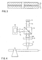
- FIGS. 1 and 2 are schematic views for sequentially explaining processes for manufacturing an optical disk to which the embodiments of the present invention can be applied.
- a glass plate having, for example, a diameter of 220 mm and a thickness of 6 mm is prepared, and a glass base plate 101 is obtained after a surface thereof is polished to a predetermined surface roughness and cleaned.
- a photoresist 102 is applied to the surface of the glass base plate 101 as shown in FIG. 1B, and then patterns 103 composed of guide grooves (concavo-convex portions), pits and the like is exposed using a base plate exposing machine using a gas laser having a wavelength of, for example, 351 nm as a light source as shown in FIG. 1C.
- the exposed glass base plate 101 is developed with an alkaline developer so as to eliminate the undeveloped portion of the photoresist, and patterns 104 composed of pits and the like is obtained as shown in FIG. 1D.
- Ni or the like for example, is plated on the glass base plate 101, and a stamper 105, to which the pattern 104 has been transferred, is obtained by exfoliating the Ni plating from the glass base plate 101.
- the stamper 105 is set to an injection molding machine 201, and injection molding is executed using the stamper 105 as a mold, thereby a resin molded plate, onto which the predetermined patterns composed of the guide grooves (concavo-convex portions, i.e., lands and grooves), the pits, and the like have been transferred, is obtained (the resin molded plate corresponds to a first substrate 1a or a second substrate 1b of an optical disk that will be explained below using FIG. 3).
- the substrate (the resin molded plate 1a or 1b) is formed of polycarbonate.
- a metal or alloy film 2 is formed by, for example, a sputtering device or a dye film 2 is coated by a spinner according to a use of the optical disk and a type of the first and second substrates.
- the optical disk is a DVD-ROM
- an Al or Ag reflection film 2 is formed, and when it is a DVD-RAM, a multi-layer recording film 2 is formed.
- the substrate (1a or 1b) is mounted on the turntable of a spinner (not explained in detail), and a UV curing resin (not shown), which is cured by, for example, ultraviolet rays irradiated thereto, is applied to the substrate as a bonding agent.
- the second substrate (1b) which is previously prepared in a different process, is set on the substrate (1a) and irradiated with ultraviolet (UV) rays (not explained in detail), thereby the_two substrates (1a and 1b) are bonded to each other.
- UV ultraviolet
- the substrates 1a and 1b are molded, parameters, for example, the temperatures of the resin material and the stamper (mold) 5, a pressure when the resin material is injected, a cooling time, a mold separating speed when a mold is separated, and the like are optimized. With the above optimization, characteristics such as a pattern transferring property to the respective substrates (1a and 1b), the curling of a single substrate, the magnitude of double refraction in the substrates, the thicknesses of the substrates, and the like are set to predetermined values.
- FIG. 5 is a schematic view showing an example of an optical disk apparatus that records information on the optical disk explained in FIG. 3 and reproduces the information recorded on the optical disk.
- the optical disk apparatus 20 records the information, that is, data on the optical disk 1 which is the information recording medium or reproduces the data recorded on the optical disk 1.
- the optical disk apparatus 20 includes an optical pickup (optical head) 21, a signal detection unit 22, which receives the laser beam reflected from the optical disk 1 and outputs a current having a magnitude corresponding to the intensity of the laser beam, a level slice signal processing circuit 23, a PRML (partial response and maximum likelihood) signal processing circuit 24, a signal determination circuit 25, a drive control circuit 26, an error correction unit 27, a host apparatus interface 28, a modulator 29, a write compensation circuit 30, a write driver 31, a servo controller 32, a spindle motor 33, and the like. Note that since the error correction unit 27, the host apparatus interface 28, and the modulator 29 are not components to which the embodiments of the present invention directly relate, the detailed explanation thereof is omitted.
- the optical pickup 21 shown in FIG. 5 includes a semiconductor laser element (hereinafter, abbreviated as laser element) 11 that can emit a laser beam (light beam) having a predetermined wavelength, for example, a wavelength of 405 nm, an objective lens 12, which converges the laser beam emitted from the laser element 11 on the recording surface of the optical disk 1, a photo-detector 13 (signal detection unit 22), which receives the light (laser beam) reflected from the recording surface of the optical disk 1 and outputs a current corresponding to the intensity of the reflected light, and the like, as explained in FIG. 4.
- laser element semiconductor laser element
- the optical disk 1 is set to a clamper (not shown) of the spindle motor 33 and turned by the spindle motor 33 so that a speed per a unit length of a pit (mark) train which indicates information has the same speed over the entire region of the optical disk 1.
- a polarized beam splitter 14 and a retarder (quarter-wave plate) 15 are interposed between the objective lens 12 and the laser element 11.
- the polarized beam splitter 14 separates the light, which is directed from the laser element 11 to the optical disk 1, from the light, which is reflected on the recording surface of the optical disk 1, making use of reflection and transmission that depend on the direction of the polarizing surface of the laser beam, and the retarder (quarter-wave plate) 15 aligns the isolation between the light directed from the laser element 11 to the optical disk 1 and the light reflected on the recording surface of the optical disk 1.
- the laser element 11 has a laser driver (not shown) and a write driver 31 connected thereto.
- the laser driver causes the laser element 11 to output a laser beam having a predetermined intensity
- the write driver 31 varies the intensity of the laser beam output from the laser element 11 according to the presence or absence of information to be recorded.
- the laser beam output from the laser element 11 is converged onto the recording surface of the optical disk 1 through the objective lens 12.
- the optical disk 1 is an optical disk on which information can be recorded only once
- a pit (mark) train is formed on the optical disk 1 by the converged laser beam when information is recorded.
- the phase of the optical disk 1 is varied when the information is recorded and a pit (mark) train is formed on the optical disk 1.
- the pit (mark) train indicates information by the intervals between marks and the lengths of the respective marks.
- the polarizing direction of the laser beam reflected by the optical disk 1 is varied depending on the presence or absence of the pit (mark) train.
- the laser element 11 outputs a laser beam whose intensity corresponds to the magnitude of a laser drive current supplied from the write driver 31 according to an indication (power) set by the write compensation circuit 30.
- a laser beam which has the intensity of any of a reproducing power for obtaining a reproduced signal, a recording power for recording information, and an erasing power for erasing information, is output.
- the signal detection unit 22 (photo-detector 13) of the optical pickup 21 includes current/voltage converters (amplifiers) 41a, 41b, 41c, 41d, an adder 42a, an adder 42b, a subtracter 43, and the like.
- the current/voltage converters 41a, 41b, 41c, 41d convert the each detection signal (Ia, Ib, Ic, Id), which is supplied from arbitrary detecting regions (which are divided into four regions in this example, and the respective detecting regions are denoted by 13a, 13b, 13c, and 13d in a clockwise direction from the upper left detecting region 13a) of the photo-detector 13 acting as a photo-detector for detecting the laser beam, into the voltage signals from the current signals.
- the adder 42a adds the signals from the amplifiers 41a and 41b
- the adder 42b adds the signals from the amplifiers 41c and 41d
- the subtracter 43 subtracts the signal from the adder 42a by the signal from the adder 42b.
- the signal from the subtracter 43 that is, the signal output from the signal detection unit 22 is supplied to the level slice signal processing circuit 23 and the PRML signal processing circuit 24 that reproduce data.
- the level slice signal processing circuit 23 includes an AGC (automatic gain control) amplifier 51, an adder 52, an equalizer 53, a level slice detector 54, a PLL circuit 55, a RLL demodulator 56, an AGC controller 57, an offset controller 58, and the like.
- AGC automatic gain control
- the level of the signal supplied from the signal detection unit 22 (output obtained by subjecting the light reflected from the optical disk 1 to photoelectric conversion) is corrected by the AGC amplifier 51 based on the control signal from the AGC controller 57 and supplied to the adder 52.
- the signal whose gain has been controlled by the AGC amplifier 51 is added to the offset signal from the offset controller 58 by the adder 52 and supplied to the equalizer 53.
- the signal, to which the offset signal has been added by the adder 52, is subjected to waveform equalization (processing) by the equalizer 53 so that the intersecting point of a threshold value, which is previously set to the waveform (reproduced waveform) of a reproduced signal, and an equalized signal is caused to coincide with (or to approximate to) the center of a window, and then the signal is supplied to the level slice detector 54, the AGC controller 57, and the offset controller 58.
- the level slice detector 54 detects the intersecting point of the equalized waveform from the equalizer 53 and the threshold value based on the channel clock from the PLL circuit 55, and when the intersecting point is detected in the window, binary data "1" is supplied to the RLL demodulator 56, and when the intersecting point is not detected in the window, binary data "0" is supplied to the RLL demodulator 56.
- the PLL circuit 55 creates the channel clock based on the signal from the level slice detector 54 and supplies the channel clock to the RLL demodulator 56.
- the RLL demodulator 56 demodulates the binary data from the level slice detector 54 based on an RLL code.
- the AGC controller 57 sets an amount of correction in the AGC amplifier 51 based on the equalized waveform output whose waveform has been equalized by the equalizer 53.
- the offset controller 58 supplies an offset value, which has been based on the equalized waveform output from the equalizer 53, to the adder 52.
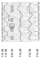
- FIG. 8A shows recording data
- FIG. 8B shows a recording waveform
- FIG. 8C shows the positional relationship between pits and a laser beam
- FIG. 8D shows a reproduced waveform (which is an output from the signal detection unit 22)
- FIG. 8E shows an equalized waveform
- FIG. 8F shows intersecting point detecting binary data, respectively.
- a pit (mark) train as shown in FIG. 8 is previously formed on the optical disk 1 according to the recording waveform of NRZI (Non Return to Zero Inverted) form (FIG. 8B) which is caused to correspond to the recording data (FIG. 8A) that is information to be recorded.
- NRZI Non Return to Zero Inverted
- a reproducing laser beam is irradiated onto the pit (mark) train of the optical disk 1 from the laser element 11 of the pickup 21 as a beam spot shown by slanted lines in FIG. 8C.
- a reflected laser beam in which a refection factor or the direction of polarized light in the beam spot is varied according to the presence or absence of pits, can be obtained.
- the reflected laser beam is received by the signal detection unit 22 shown in FIG. 5 and subjected to signal processing, thereby the information recorded on the optical disk 1 is read out. That is, a reproduced signal, which corresponds to the information recorded on the optical disk 1, can be obtained from the output that is obtained by subjecting the laser beam reflected from the optical disk 1 to a photoelectric conversion by the photo-detector 13 shown in FIG. 4.
- the waveform (reproduced waveform) of the reproduced signal from the signal detection unit 22 (photo-detector 13) is not formed in a rectangular waveform as the recorded waveform explained before using FIG. 8B due to the characteristics of a recording/reproducing system and is formed in a dull waveform as shown in FIG. 8D.
- the waveform (reproduced waveform) of the reproduced signal shown in FIG. 8D is subjected to the waveform equalization (processing) by the equalizer 53 so that the intersecting point of a threshold value (shown by a dot-dash-line in FIG. 8F) previously set to the waveform (reproduced waveform) of a reproduced signal, and an equalized signal is caused to coincide with (or to approximate to) the center of a window as shown in FIG. 8E.
- the high frequency component of the reproduced signal is amplified.
- the waveform (reproduced waveform) of the reproduced signal which has been subjected to the equalization processing, is binarized as "1" when the intersecting point of the equalized waveform and the threshold value is detected by the level slice detector 54 in a window as shown in FIG. 8F and is binarized as "0" when the intersecting point is not detected therein.
- a demodulated signal which is obtained by demodulating the binary data obtained by the level slice detector 54, is output from the RLL demodulator 56.
- the PRML signal processing circuit 24 includes an AGC amplifier 61, an adder 62, an A/D converter 63, a linear equalizer (equalizer) 64, an ML decoder (Viterbi decoder) 65, an RLL demodulator 66, a PLL circuit 67, an AGC controller 68, an offset controller 69, and the like.
- the level of the signal supplied from the signal detection unit 22 (output obtained by subjecting the light reflected from the optical disk 1 to photoelectric conversion) is corrected by the AGC amplifier 61 based on the control signal from the AGC controller 68 and supplied to the adder 62.
- the signal whose gain has been controlled by the AGC amplifier 61 is added to the offset signal from the offset controller 69 by the adder 62 and supplied to the A/D converter 63.
- the signal, to which the offset signal has been added by the adder 62, is converted into a digital signal by the A/D converter 63 by being converted into a discrete time and a,discrete amplitude value series based on the channel clock from the PLL circuit 67 and supplied to the linear equalizer 64.
- the digital signal output from the A/D converter 63 subjected to equalization processing by the linear equalizer 64 which includes an FIR filter (transversal filter) and the like, so that the waveform of the digital signal has PR(1,1) characteristics with respect to the waveform (reproduced waveform) of the reproduced signal, and the digital signal is supplied to the ML decoder 65, the PLL circuit 67, the AGC controller 68, and the offset controller 69.
- the equalized waveform from the equalizer 64 is decoded by the ML decoder 65 and supplied to the RLL demodulator 66 as binary data.
- a Viterbi decoder for example, can be used as the ML decoder 65.
- the RLL demodulator 66 demodulates the decoded binary data output from the ML decoder 65 based on the RLL code.
- the PLL circuit 67 creates the channel clock based on the equalized waveform output from the linear equalizer 64, and the channel clock is supplied to the A/D converter 63. That is, the PLL circuit 67 converts the difference between the amplitude value of a PR equalized waveform and the ideal amplitude value thereof into a difference of phase, thereby the channel clock is recovered (demodulated).
- the AGC controller 68 sets the amount of correction (gain control level) in the AGC amplifier 61 based on the equalized waveform output from the equalizer 64.
- the offset controller 69 sets an offset value to be supplied to the adder 62 based on the equalized waveform output from the equalizer 64.
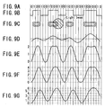
- FIG. 9A shows recording data
- FIG. 9B shows a recording waveform
- FIG. 9C shows the positional relationship between pits and a laser beam
- FIG. 9D shows a reproduced waveform (which is an output from the signal detection unit 22)
- FIG. 9E shows the PR(1, 1) characteristics
- FIG. 9F shows PR(1, 2, 1) characteristics
- FIG. 9G shows PR(1, 2, 2, 1) characteristics, respectively.
- a pit (mark) train is previously formed on the optical disk 1 according to the recording waveform NRZI form (FIG. 9B) which is caused to correspond to the recording data (FIG. 9A) that is information to be recorded.
- a reproducing laser beam is irradiated onto the pit train of the optical disk 1 from the laser element 11 of the pickup 21 as a beam spot shown by slanted lines in FIG. 9C.
- a reflected laser beam in which a refection factor or the direction of polarized light in the beam spot is varied according to the presence or absence of pits, can be obtained.
- the reflected laser beam is received by the signal detecting section 22 shown in FIG. 5 and subjected to signal processing, thereby the information recorded on the optical disk 1 is read out. That is, a reproduced signal, which corresponds to the information recorded on the optical disk 1, can be obtained from the output that is obtained by subjecting the laser beam reflected from the optical disk 1 to a photoelectric conversion by the photo-detector 13 shown in FIG. 4.
- a reproduced waveform which is a dull waveform as compared with the recording data (FIG. 9A) due to the characteristics of a recording/reproducing system, is equalized by the equalizer 64 explained before using FIG. 8 according to the PR(1, 1) characteristics, the PR(1, 2, 1) characteristics, and the PR(1, 2, 2, 1) characteristics, respectively.
- PR(1,1) characteristic is a characteristic in which an impulse response appears at the rate of 1:1 at two successive identification points (that is, amplitude values of the reproduced waveform at two channel clock timings), respectively.
- the recording waveform of NRZI form of FIG. 9B corresponding to the first part "010010" of recording data of FIG. 9A is expressed as follows. 011100
- the waveform of FIG. 9E expressed as linear superposition of the following responses and obtained as "012210” becomes a target waveform to be equalized as the PR(1,1) characteristic (class).
- 0110 00110 000110 PR(1, 2, 1) characteristic is a characteristic in which an impulse response appears at the rate of 1:2:1 at three successive identification points (that is, amplitude values of the reproduced waveform at three channel clock timings), respectively.
- PR(1,2,2,1) characteristic is a characteristic in which an impulse response appears at the rate of 1:2:2:1 at four successive identification points (that is, amplitude values of the reproduced waveform at four channel clock timings), respectively.
- to-be-equalized target waveforms derived by linear superposition of impulse responses corresponding to the recording waveform become the waveforms as shown in FIGS. 9F and 9G (although not shown, this is also applied to other PR characteristics).
- an increase in the signal degrading component in the equalizer 64 can be suppressed by equalizing the reproduced waveform, which is obtained by converting the laser beam reflected from the optical disk 1, into a waveform of a PR characteristic that is closer to the characteristics of of the reproduced waveform.
- the equalized waveform from the equalizer 64 is decoded by the ML decoder 65 and supplied to the RLL demodulator 66 as the binary data.
- the ML decoder 65 selects a series having the smallest error with respect to the sample series of the equalized waveform from all of the reproduced waveform series which satisfy the PR(1,2,2,1) characteristic and estimates and outputs recording data (binary data, decoded data) used as a source for generating the selected reproduced waveform series while tracing the state transition.
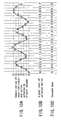
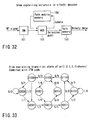
- FIGS. 10A to 10C are schematic views explaining an example of decoding executed by the ML decoder 65.
- the decoding process is not executed based on one sample value but executed based on a sequence using the correlation (waveform interference) due to the PR characteristic of a series of a plurality of sample values as a premise. Accordingly, the PRML system is highly resistant to the signal degrading component having no correlation between sample values.
- the decoded data as shown in FIG. 10C i.e., the same data as that of FIG. 9A can be obtained by deriving "the signal level of the selected series" shown in FIG. 10B based on the correlation between "the sample series of the equilized signal” as shown in FIG. 10A and "the series selected by the ML decoder 65".
- the reproduced waveform of the ideal PR characteristic obtained by linear superposition of the above impulse responses is obtained as follows. 0135531 ...
- the number of candidates of the waveform can be increased and counted up as in a tree structure.
- the number of available states is limited when taking the PR characteristic into consideration.
- the constraint length (the range which the waveform interference gives an influence) is "4", and variations of recording data series caused by the waveform interference occur in 16 combinations of four-digit values constructed by two types of data values of "0" and "1", and therefore, the state number having no redundancy is 16 at maximum. There is a possibility that the state number will be reduced if the modulation code is limited.
- the ML decoder 65 calculates the probability according to an input sample value when it is assumed that the state is transited from a certain state to a next state. When a plurality of candidates of the waveform series transited to the same state are provided, a probable one of the candidates is determined based on the accumulated value of the past transition probability.
- the ML decoder 65 is provided with a path memory (which will be described later using FIGS. 30 to 34) that stores candidates of the waveform series. Generally, the length thereof is set to a length of several ten channel bits. A plurality of candidates of the waveform series are transited to the same state while they pass through the path memory, then the candidates are repeatedly selected and the most probable series is finally selected.
- the ML decoder 65 includes a branch metric calculation unit, an ACS, which is the abbreviated name of an add-compare-select block circuit, and a path metric memory.
- the branch metric calculation unit calculates a logarithm value of the probability of transition of the state which is expressed in terms of a difference between actual amplitude and ideal amplitude obtained if it is assumed that the state is transited from a certain state to a next candidate state when a sample value is input, and the path metric memory is a memory for storing a past branch metric accumulated value obtained until the state transition for each of the states of the state number is repeatedly executed and the state is attained. Since it is well known that the most probable series is selected by the ML decoder, it is not explained here in detail.
- the signal determination circuit 25 is used to switch between the slice system and the PRML system shown in FIG. 7.
- the PRML system can reproduce a signal even if the shortest mark/pit has a small amplitude value.
- the level slice system since the amplitude value of the shortest mark/pit is required to be larger than a certain level, this system is disadvantageous in a series is which a signal intensity is reduced.
- the conditions and the characteristics, which are preferable to reproduce a signal from the optical disk 1 are confirmed by the signal determination circuit 25 based on the signals that are obtained by processing a reproduced waveform by both the PRML system and the level slice system. Accordingly, the information recorded on the optical disk 1 is reproduced by the characteristics inherent to the optical disk 1 and the preferable reproducing conditions required to reproduce a signal.
- the drive control circuit 26 can output a selection signal for switching whether a signal is to be reproduced by the PRML signal processing circuit 24 or by the level slice signal processing circuit 23 based on the output from the signal determination circuit 25, that is, based on the signal output from at least any one of the PRML signal processing circuit 24 and the level slice signal processing circuit 23.
- a changeover switch 59 of the level slice signal processing circuit 23 is turned on in response to the selection signal supplied thereto from the drive control circuit 26, thereby signal reproduction from the reproduced waveform, which is executed by the level slice signal processing circuit 23, is selected.
- a changeover switch 59 of the PRML signal processing circuit 24 is turned on in response to the selection signal supplied thereto from the drive control circuit 26, thereby signal reproduction from the reproduced waveform, which is executed by the level slice signal processing circuit 23, is selected.
- the drive control circuit 26 outputs a predetermined control command to the servo controller 32 based on the address data that is related to the data obtained by the data instructed from the host apparatus interface 28 and the data obtained by the error correction unit 27. With this operation, the optical pickup 21 is moved to a predetermined position as well as the number of rotation of the spindle motor 33 is set to the number of rotation of a zone corresponding to an access position.
- the laser beam emitted from the laser element 11 as a light source is guided to the objective lens 12 passing through the polarized beam splitter (PBS) 14 and the quarter-wave plate 15.
- the laser beam guided to the objective lens 12 is converged to a predetermined position of the optical disk 1, that is, to a predetermined depth of a track or a groove by a converging property given to the laser beam by the objective lens 12.
- the component which is guided to the optical disk 1, of the laser beam emitted from the laser element 11, is an electric field component (P polarized light) whose polarizing surface is parallel with the incident surface of the PBS 14, and an electric field component (S polarized light) whose polarizing surface is vertical to the incident surface is reflected by the reflection PBS.
- P polarized light an electric field component whose polarizing surface is parallel with the incident surface of the PBS 14
- S polarized light an electric field component polarized light
- the quarter-wave plate 15 is a sheet-like member formed by cutting an optical crystal having a predetermined double refraction value to a predetermined thickness corresponding to the wavelength of a laser beam and converts the linear polarized light of P polarized light, which has been emitted from the laser element 11 and passed through the PBS 14, into circular polarized light and converts the circular polarized light of the laser beam reflected by the optical disk 1 into linear polarized light.
- the laser beam from emitted the laser element 11 passes through the PBS 14 as it is and is incident on the objective lens 12 after the direction of the polarized light surface thereof converted into circular polarized light by the quarter-wave plate 15.
- the reflected laser beam which has been reflected by the optical disk 1 and returned to the objective lens 12 and the direction of the polarized light of which is the circular polarized light, is caused to pass through the quarter-wave plate 15 again, thereby the reflected laser beam is made to linear polarized light the direction of the polarized light is directed to the y-axis direction.
- the reflected laser beam from the optical disk 1, which has been returned to the PBS 14, is reflected to the photo-detector 13 by the PBS 14, subjected to photoelectric conversion by the photo-detector 13 and used to output a reproduced waveform for obtaining a reproduced signal.
- the intensity of the laser beam, which returns to the laser element 11, of the reflected laser beam is sin 2 ( ⁇ /2) times compared with the intensity of the laser beam directed from the laser element 11 to the optical disk 1. Accordingly, the intensity of the laser beam reflected toward the photo-detector 13 by the PBS 14 is cos 2 ( ⁇ /2) times.
- the phase retardation ⁇ due to the double refraction is "0"
- the reflected laser beam is entirely incident on the photo-detector 13
- the intensity of the laser beam incident on the photo-detector 13 is reduced by 1-sin 2 ( ⁇ /2). Since the laser beam returned to the laser element 11 also acts as a factor for increasing the noise of the laser beam, it must be suppressed as small as possible.
- the laser beam Ein which is emitted from the laser element 11 and incident on the PBS 14, is represented by Expression (1) shown below.
- the laser beam Ein is represented by Expression (2) shown below.
- the laser beam Eout 1 Since the phase of the y-directional component of the laser beam Eout 1 , which has passed through the quarter-wave plate 15, is retarded by ⁇ /2, the laser beam Eout 1 is represented by Expression (3) shown below.
- the reflected laser beam Eref is represented by Expression (5) shown below.
- the reflected laser beam Eref When the reflected laser beam Eref is caused to pass through the quarter-wave plate 15 once more, it becomes a reflected laser beam Eout 2 the phase of the y-directional component of which has been retarded by ⁇ /2, and the reflected laser beam Eout 2 is represented by Expression (7) shown below.
- Equation (9) the intensity Ix of the return laser beam, which has passed through the reflected laser beam PBS 14 and has been returned to the laser element 11, of the laser beam Eout 2 that had been returned to the PBS 14, is represented by Equation (9) shown below
- Ix a 2 sin 2 ( ⁇ /2)
- Iy a 2 cos 2 ( ⁇ /2)
- the intensity of the reflected laser beam incident on the photo-detector 13 is cos 2 ( ⁇ /2) times that of the intensity of the laser beam directed from the laser element 11 to the optical disk 1.
- the following upper limit is set as the magnitude of the double refraction ⁇ when it is measured using a double pass to suppress the reduction of intensity of the signal detected by the photo-detector 13.
- the upper limit is set, for example, to:
- Standard ECMA-267 shows "to measure the double refraction by irradiating a laser beam having a wavelength of 640 ⁇ 15 nm at an angle 7° with respect to the direction vertical to a disk" on pages 41 and 42.
- the relationship between the double refraction ⁇ and the intensity of the laser beam incident on the photo-detector 13 is represented by Table 1 shown below.
- Double refraction (nm) Signal intensity (%) 0 100.0 10 99.8 20 99.1 30 97.9 40 96.3 50 94.3 60 91.8 70 89.0 80 85.8 90 82.3 100 78.4
- a signal in a system in which a signal amplitude (signal intensity) decreases, a signal is generally amplified by an amplifier.
- simply amplifying the signal is not effective because a noise component is increased at the same time and a C/N (S/N) ratio remains unchanged.
- a reproduced waveform can be detected at a higher error rate using a ML detector that selects the most reliable sequence from the sequences that takes the front and the back of a waveform into consideration.
- binary data is determined based on the position of the intersecting point of a threshold value set to a reproduced waveform and an equalized waveform, the intersecting point being detected by being subjected to equalization processing to dispose the interesting point at the center of window, decoded data is obtained by subjecting the binary data, which has been obtained by detecting the intersecting point, to NRZI (Non Return to Zero Inverted) conversion (data recorded on an optical disk is decoded).
- NRZI Non Return to Zero Inverted
- the intersecting point of the equalized waveform and the threshold value is not always the center of a window because of noise and the like.
- the standard deviation of the data at the intersecting point is called a jitter when it is standardized using a window width, and the jitter is used as an evaluation reference of optical discs and optical disk drives.
- a higher track density causes a reproduced signal to include a larger amount of a signal deteriorating component called a crosstalk component.
- a higher line density results in a duller reproduced waveform.
- the high frequency component of the reproduced signal is amplified by the equalizer as described above, when an input reproduced waveform is a duller reproduced waveform, the high frequency component must be more amplified. As a result, it is apparent that the signal deteriorating component described above is also amplified by the equalizer.
- the signal intensity is reduced up to 78.4% in the DVD-ROM and the DVD-R and up to 91.8% in the DVD-RAM by the effect of the double refraction ⁇ described before using Table 1.
- the standard value (100 nm) of the double refraction of the DVD-ROM and the DVD-R is applied as it is from Table 2, the signal intensity is halved in the DVD-ROM and the DVD-R and reduced to about 80% in the DVD-RAM in which the standard value of the double refraction is 60 nm. Accordingly, a problem arises in that when information is recorded and reproduced, an error tends to occur and the information cannot be accurately recorded and reproduced.
- a first point is a case of using the waveform slice system, which is utilized at present, as a signal processing system when a signal is recorded on and reproduced from an optical disk of the DVD standard.
- the limit value of the double refraction can be examined by the same concept as that used in the optical disk of the DVD standard.
- the values of the double refraction ⁇ which satisfy the allowable ranges of the signal intensity of the DVD standard optical discs determined from Table 1 (the signal intensity of DVD-ROM and DVD-R: 78.4 or more, and the signal intensity of DVD-RAM: 91.8% or more) also in a system using the laser beam having the wavelength of 405 nm, are determined from Table 2 the value of the double refraction ⁇ is 60 nm or less in a ROM (reproduction-only) disk and an R (recordable only once) disk and 40 nm or less in a RAM (recordable and erasable) disk (hereinafter, referred to as a recording/reproducing optical disk).
- a second point is a case of using the PRML system that is effective as a reproduced signal processing system when the S/N (signal to noise ratio) of a reproduced signal is lowered.
- the level of the reproduced signal can be increased by about 2 dB in terms of the S/N ratio by the effect of the ML determination circuit explained before using particularly FIGS. 6, 7, and 9. This means that a reproduced signal of the same level can be obtained by signal intensity of about 80% as compared with a case that ML is not determined when it is examined in terms of a signal amplitude.
- using the PRML system permits information to be stable recorded and reproduced when a signal amplitude is 80% of that in the waveform slice system.
- the PRML system is used, if a signal amplitude of 90% of that in the waveform slice system is obtained, the information can be stably recorded and reproduced.
- signal intensity (62.7% or more in ROM and R discs and 73.4% or more in a RAM disk) that is 80% of the allowable ranges of the signal intensity in the DVD standard optical discs that can be determined from Table 1 (78.4 or more in DVD-ROM and DVD-R, and 91.8% or more in DVD-RAM) is the lower limit value of the signal intensity required to reproduce a signal.
- the value of the double refraction which can secure the signal intensity acting as the lower limit value of the DVD standard optical discs is determined using Table 2, the value is 85 nm or less in the ROM and R discs and 70 nm or less in the R disk.
- the value of the double refraction which can secure the signal intensity (70.6 or more in DVD-ROM and DVD-R, and 82.6% or more in DVD-RAM) which is 90% of that in the allowable range of the signal intensity in the DVD standard optical discs as the level of the value of the double refraction that can preferably secure the signal intensity
- the value is 75 nm or less in the ROM and R discs and 55 nm or less in the RAM disk.
- the PRML system when used in the signal processing, even if the signal intensity is lowered by the effect of the double refraction described above in an optical disk, which can record and reproduce information by the laser beam having the wavelength of 405 nm, and in an optical disk apparatus, which can record and reproduce information on and from an optical disk, the information can be securely recorded and reproduced.
- optical disk which is formed by the processes described above with reference to FIGS. 1A to 1E and FIGS. 2A to 2C, will be explained in detail using FIG. 3.
- the optical disk 1 is made by forming a metal film or a dye film (a reflection film in an reproduction-only disk, an organic recording layer in an only-once-recordable disk, and a phase varying recording film in a rewritable disk) 2 on the molded substrate 1a made in the molding processes of FIG. 1, and then another molded substrate (or dummy substrate) 1b is bonded on the molded substrate 1a using ultraviolet curing resin that is not described in detail.
- a hard coat layer which is not described in detail, is formed on the laser beam incident surface of the molded substrate 1a to protect the disk from scratch and dirt.
- the recording layer 2 which is the metal film or the dye film
- the recording layer 2 is formed in the thickness of about 100 nm by sputtering or vacuum depositing a metal such as Al, Ag, etc.
- a dye material which can securely absorb the 405 nm laser beam, is coated in the thickness of 100 nm by, for example, spin coating.
- the recording layer 2 is the phase varying recording film, which is used in the recording/reproducing disk, a film of a predetermined metal or alloy is formed by sputtering and the like.
- the ultraviolet ray curing resin 3 is coated on at least one resin molded sheet (substrate 1a or 1b) in a state that it is placed on a spinner (that is not described in detail). Then, after the confronting substrate is set to the resin molded sheet, the resin molded sheet is left in vacuum to remove the bubbles contained in the ultraviolet ray curing resin 3. Subsequently, after the ultraviolet ray curing resin 3 is pressed with a predetermined pressure, it is irradiated with ultraviolet rays and cured.
- Resin having viscosity of about 400 cps can be used as the ultraviolet ray curing resin, and a resin SD649 manufactured by Dainippon Ink and Chemicals, Incorporated, for example, is used in this embodiment.
- the number of rotation of the spinner is set to 60 RPM when the ultraviolet ray curing resin is dropped and to 8000 RPM when the resin is splashed, thereby an about 25 ⁇ m thick resin layer is obtained.
- the resin molded sheet (the substrate 1a or 1b or the dummy substrate) is injection molded by, for example, a DVD injection molding machine (IS40HD) manufactured by Toshiba Machine Co., Ltd.
- a plycarbonate resin (AD-5503) manufactured by Teijin Chemicals Ltd., for example, can be used as a substrate material.
- the size of the pit (mark), which can reproduce information by the laser beam having the wavelength of 405 nm is small as compared with the size of the DVD standard disk, and a track pitch is narrow likewise in the only-once-recordable disk, which can record information by the laser beam having the above wavelength, and in the recording/reproducing disk.
- the characteristics of the molded substrate depend on many parameters represented an injection pressure, a mold clamping pressure, a stroke time, a timing at which molds are clamped, a metal mold temperature and the like, attention is mainly paid to the metal mold temperature in this embodiment.
- the glass transition temperature of the polycarbonate resin as the substrate material is about 150° and an increase in the metal mold temperature is limited. However, there is a tendency that the magnitude of the double refraction is suppressed by increasing the metal mold temperature. Therefore, in this embodiment, a plurality of types of optical discs are formed by changing the metal mold temperature and evaluated by the method described below, and an optimum condition is determined by the result of evaluation.
- optical discs used as samples are as described below.
- a base plate was made as a ROM (reproduction-only) disk by a base plate exposing machine that uses a Kr laser beam having a wavelength of 351 nm, a Ni-plated stamper, on which transfer data having a shortest mark length of 0.205 ⁇ m, a track pitch of 0.40 ⁇ m, and a pit depth of 70 nm was recorded by cutting was used.
- samples A, B, C, D, E were prepared.
- Each of the substrates was formed to have an inside diameter of 15 mm, an outside diameter of 60 mm, and a thickness of 0.60 mm.
- An Al film of 100 nm thick was formed on the molded substrate by a sputtering device, and the substrate was bonded to another molded substrate through ultraviolet ray curing resin.
- the double refraction of these samples was measured at a position having a radius of 40 mm.
- the double refraction was measured by a double refraction measuring device, which was made by Admon Science, Inc. and employed a laser element capable of outputting a blue laser beam (wavelength: 400 nm) as a light source.
- the double refraction measuring device could accurately measure the change of phase of the laser beam reflected on the recording surface of a disk.
- the laser beam was incident on the disk at an angle tilted 7° from a direction vertical to the disk based on the regulation of Standard ECMA-267, p 41-42.
- the numerical aperture NA of an objective lens of an optical pickup was set to 0.65, and the signal characteristics of the laser beam reflected from the optical disk were evaluated by a laser beam having a wavelength of 405 nm. Further, to evaluate the signal characteristics, an error rate was evaluated as signal processing unique to the applicant.
- the RLL modulation was used as a data modulation system in the present invention, it is needless to say that the same effect could be obtained by another modulation system.
- the sample disk was turned so that a pit (mark) train was moved at a line speed of 6.6 m/sec and the read power of the laser beam was set to 0.5 mW, and a reflected laser beam was obtained from precut data by setting the read power of the light beam to 0.5 mW.
- the double refraction was measured by a method of measuring the level of an RF signal on the high reflection ratio side thereof as Rtop and determining the error rate of decoded data by the signal processing circuit 25 explained before with reference to FIG. 6.
- the error rate was determined by being measured by the level slice system and the PRML system which were arbitrarily switched by the signal determination circuit 25.
- the magnitude of the double refraction determined based on the reflected laser beam obtained by turning the sample disk was used as the average value of the double refraction in the one round of the disk.
- Table 3 shows a result of evaluation obtained by capturing the laser beams reflected from the sample discs A to E described above to a signal evaluation device.
- Rtop shows a value standardized using the value of the sample A (double refraction ⁇ is generally "0") as a reference.
- the error rate a threshold value in which a signal can be stably reproduced is set to 1 ⁇ 10 -4 , and an error rate equal to or less than the threshold value is shown by ⁇ and an error rate exceeding the threshold value is shown by ⁇ .
- Table 4 relates to a recording/reproducing disk on which information can be rewritten.
- Five kinds of samples whose injection condition was changed similarly to the ROM disk described above were prepared, and Table 4 shows a result of evaluation of the effect of double refraction to these samples.
- a base plate and a stamper were made similarly to those of the ROM disk, a groove (land) pitch was set to 0.68 ⁇ m, and data was recorded in grooves and lands (a track pitch was set to 34 ⁇ m. Further, the grooves were composed of a continuous spiral groove directed from the inner radius of the disk to the outer radius thereof.
- FIG. 11 shows an example of a multi-layer recording film common to the five kinds of the sample discs shown in Table 4.
- the layers from the first dielectric layer 3 to the refection layer 7 are formed by sputtering.
- the first dielectric layer 3 has a thickness of 30 nm
- the second dielectric layer 4 has a thickness of 60 nm
- the third dielectric layer has a thickness of 35 nm
- the recording layer 2 has a thickness of 15 nm
- the fourth dielectric layer 6 has a thickness of 30 nm
- the reflection layer has a thickness of 100 nm.
- the evaluation condition of the RAM disk As the evaluation condition of the RAM disk, the effect of double refraction on a reflected laser beam, which was obtained when data was recorded first and then the recorded data was reproduced, was evaluated.
- the recorded data was random data subjected to the RLL modulation.
- a laser waveform modulated for recording as shown in FIG. 12 was used to record the data.
- Pw denotes a write power
- Pe denotes an erase power
- Pr denotes a reproduction power, respectively.
- data could be overwritten by optimizing the respective powers.
- Pe 2.4 mW
- Pr 0.5 mW.
- a line speed was set to 5.6 m/sec
- a channel frequency was set to 64.8 MHz in recording.
- Rtop shows a value that is standardized using the value of the sample A (double refraction ⁇ is generally "0") as a reference.
- a threshold value in which a signal can be stably reproduced is set to 1 ⁇ 10 -4 , and an error rate equal to or less than the threshold value is shown by ⁇ and an error rate exceeding the threshold value is shown by ⁇ .
- the system explained before with reference to FIG. 6 is used as the signal processing circuit.
- a base plate and a stamper each having a track pitch of 0.40 ⁇ m and a groove depth of 100 nm were formed by manufacturing processes similar to those of the recording/reproducing disk explained before. Then, samples each of which was composed of two substrates having a dye film formed thereon were prepared, and the signal intensity of a reflected laser beam was evaluated in the respective sample discs similar to the ROM and RAM discs.
- Cyanine dye was coated by a spinner in the thickness of about 200 nm as the dye film, and an Ag film was formed in the thickness of about 100 nm by sputtering as a reflection film. Since the magnitude of the double refraction of the samples was larger than that of the RAM discs, the samples, which had the distribution of the double refraction similar to that of the ROM discs described above using Table 3 could be obtained.
- an optical disk from which information can be reproduced by a laser beam having a wavelength of 405 nm and on which information can be recorded by the laser beam having the same wavelength
- an optical disk apparatus which records information on the optical disk and reproduces information from the optical disk, inherent information is previously recorded on the optical disk itself. Further, the optical disk apparatus can optimize a recording condition and a reproducing condition by reproducing the information recorded on the optical disk.
- the optical disk 1 has a data arrangement structure that is common to each of 1) a ROM (reproduction-only) disk, 2) a write-once type (R) disk on which information can be recorded only once, and 3) a RAM (recording/reproducing type, i.e. rewritable type) disk. That is, this embodiment places greater emphasis on the securement of compatibility among information recording mediums (optical discs 1) that are classified into a reproduction-only type, a write-once type, and a rewritable type, and the information recording mediums have a common structure in the respective types described above in the following points shown in FIG. 13:
- the system lead-in areas are formed only in two reproduction-only layers (opposite track paths). Note that the arrangement of the data area of a disk including the lead-in areas is as shown in, for example, FIG. 15.
- the information area in the disk is divided into the following five sections according to the mode of the disk. That is, the disk has the system lead-in area, the connection area, the data lead-in area, the data area, and the data lead-out area.
- the information area has a track composed of an embossed-pit train.
- the track in the system lead-in area is a continuous spiral track having one round of 360°.
- the track of each of the data lead-in area, the data area, and the data lead-out area is a continuous spiral track having one round of 360°.
- the center of the track coincides with the center of the pits.
- the lead-in area is also provided with any of the reproduction-only type, write-once type, and rewritable type information recording mediums. Further, a pit region, which is called an embossed lead-in area and formed in a fine concavo-convex shape, exists in the rewritable type information recording mediums (DVD-RAM disk and DVD-RW disk) and the write-once type information recording medium (DVD-R disk) in the DVD discs used at present.
- the depth of a pit area coincides with the depth of a pregroove (continuous groove) in the data area.
- the optimum depth of the pit is ⁇ /(4n), where ⁇ shows a wavelength in use and n shows the refraction factor of a substrate.
- the optimum depth of the pregroove is ⁇ /(5n) to ⁇ /(6n) as a condition for minimizing crosstalk (amount of leakage to a reproduced signal) from the recording mark of an adjacent track in the data area.
- the pit depth in the embossed lead-in area is set to ⁇ /(5n) to ⁇ /(6n) in accordance with the above optimum depth.
- a reproduced signal having a sufficiently large amplitude can be obtained from the pits having the depth of ⁇ /(4n) or ⁇ /(5n) to ⁇ /(6n) (because the depth of the pits is sufficiently deep).
- this embodiment is characterized in that the system lead-in area is provided with any of the reproduction-only type, write-once type, and rewritable type information recording mediums and that the track pitch and the shortest pit pitch in the system lead-in area are made greatly larger than the track pitch and the shortest pit pitch (shortest mark pitch) in the data lead-in area and the data area in order to guarantee a stable reproduced signal from the lead-in area of the write-once type information recording medium while securing the compatibility of a format.
- a reproduced signal is detected using the level slice system (reproduced analog signal is output after it is binarized.).
- the shortest pit pitch of pits which are formed in a fine concavo-convex shape, or the shortest mark pitch of recording marks, which are formed by the optical variation of the characteristics of a recording film, is near to the cutoff frequency of the characteristics of the OTF (optical transfer function) of the objective lens used in the reproducing optical head (FIG. 4). Therefore, the amplitude of a reproduced signal from the shortest pit pitch and the shortest mark pitch is greatly reduced.
- the shortest pit pitch and the shortest mark pitch are reduced, it is impossible to detect a reproduced signal by the level slice system. Further, the shortest pit pitch of the write-once type information recording medium used at present (DVD-R disk used at present) is reduced because of the reason described above, a problem arises in that a stable reproduced signal cannot be obtained from the lead-in area.
- This embodiment employs the following countermeasures to overcome the contradict problems.
- the track pitch and the shortest pit pitch can be coarsened in the system lead-in area.
- the reproduced signal is binarized by the level slice system using the level slice signal processing circuit of the signal processing circuit explained before with reference to FIG. 6.
- the mechanical dimension of the information recording medium of the embodiment coincides with that of the DVD standard disk regardless of that the recording medium is any of the reproduction-only type, write-once type, and rewritable type discs.
- the track pitch and the shortest embossed pit length of the embossed pits in the system lead-in area of the information recording medium of the embodiment are set to a value near to the size of the embossed pit in the lead-in area of the DVD standard disk, so that the new medium can be discriminated from the old medium in the apparatus even if the phenomena described in the items (a) and (b) occur to thereby permit a countermeasure to be stably executed according to a type of the medium.
- emboss-shaped pits are formed in the lead-in area of an inner peripheral portion.
- a signal is detected from the embossed pits of the lead-in area using the level slice system.
- the level slice signal processing circuit 23 shown in FIG. 7 is employed to the system lead-in area.
- the same detection circuit as that explained with reference to FIG. 7 can be also used to the embossed pits existing in the lead-in area of the inner peripheral portion of the reproduction-only DVD-ROM disk and the rewritable type DVD-RAM disk that are used at preset, which can reduce the cost of the information reproducing and information recording/reproducing apparatuses by simplifying the arrangements thereof.
- An experiment shows that even if the track pitch and the shortest pit length vary ⁇ 30%, a slice level can be stably detected by the level slice signal processing circuit 23 shown in FIG. 7.
- Slight improvements which are applied to an existing information reproducing apparatus that cannot reproduce information in the data area of the information recording medium of the embodiment, can make it possible for the existing apparatus to reproduce the information in the system read-in area of the information recording medium of the embodiment using the level slice signal processing circuit built therein.
- the existing apparatus can reproduce the information in the system read-in area of the information recording medium of the embodiment using the level slice signal processing circuit built therein.
- the PRML signal processing circuit shown in FIG. 29 is the same as the PRML signal processing circuit explained before with reference to FIG. 7 except that it is shown in more detail.
- the capacity of the information recording medium can be increased by increasing the density of the recording pits and the recording marks by using the PRML system in the signal reproduction processing.
- a reference code zone is formed in the data lead-in area of the reproduction-only information recording medium, and automatic circuit adjustment is used in a reproduction circuit shown in FIG. 29 (in particular, for the setting of respective tap coefficient values in a pre-equalizer 123, and in an AGC 124). That is, the automatic circuit adjustment is executed while reproducing the reference code beforehand to stably reproduce the information recorded on the data area and to stably detect a signal.
- the automatic adjustment accuracy of the reproduction circuit can be improved by causing the track pitch and the shortest pit length in the reference code to coincide with the value in the data area by disposing the reference code in the data lead-in area.
- FIGS. 26 and 28 show an example that a connection zone (connection area) is interposed between the data lead-in area and the system lead-in area in the recordable disk, i.e. in the write-once type (R) and rewritable type (RAM) information recording medium.
- connection area connection area
- connection zone is interposed between the system lead-in area recorded by the embossed pits and the data lead-in area recorded by the write-once or rewritable recording marks, thereby the system lead-in area is disposed apart from the data lead-in area.
- the recording type information recording medium of the embodiment has the two recording layers that can record and reproduce information only from one side.
- the laser beam reflected by the other recording layer enters a laser beam detector, from which a phenomenon called interlayer crosstalk occurs, and the characteristics of a reproduced signal are deteriorated by the crosstalk.
- the amount of reflected laser beam is greatly different depending on whether the laser beam reflected by the other recording layer is irradiated to the system lead-in area or to the data lead-in area.
- this embodiment interposes the connection zone between the system lead-in area recorded by the embossed pits and the data lead-in area recorded by the write-once or rewritable recording marks so that the system lead-in area is disposed apart from the data lead-in area, thereby the effect of the interlayer crosstalk is reduced, and thus a reproduced signal can be stably obtained.
- an initial zone and a control data zone are disposed in the system lead-in area and a buffer zone is interposed therebetween.
- the sector numbers at the start positions of the respective regions are shown on a right column of FIG. 13.
- the initial zone includes an embossed data area.
- the main data of a data frame recorded as a recorded data area in the initial zone is set to "00h".
- the buffer zone includes 32 ECC blocks (1024 sectors).
- the main data of a data frame recorded in the buffer zone as a physical sector is set to "00h".
- the control data zone includes an embossed data area.
- the data area includes an emboss control data.
- the connection region is used to connect the system lead-in area to the data lead-in area.
- the distance between the center line of a sector "02 6AFFh” at which the system lead-in area ends and the center line of a sector "02 6C00h" at which the data lead-in area starts is set from 1.4 ⁇ m to 20.0 ⁇ m as an example.
- connection area Since no physical sector number is allocated to the connection area, the connection area does not include physical sector number. All the bits of the data lead-in area excluding the reference code zone are reserved.
- the reference code zone includes embossed data segments.
- the data area includes an emboss data code.
- the reference code is composed of an ECC block (32 sectors) that starts from a sector number 1965576 ("02 FFE0h").
- the respective sectors (2048 bytes) of the main data are defined as described below according to the distribution of the main data.
- the 2048-byte sector of main data D0 to D2047, in which data symbol "164" is repeated, is created.
- the reference code for the 32 sectors is created as described below by adding scramble data to the main data of the sectors.
- the scramble data of an initial preset value "0Eh" is added to sector main data. However, the scramble data is masked to D0 to D331 of a sector 0 and is not added.
- the scramble data of the initial preset value "0Eh" is added to the sector main data.
- executing scramble twice means to execute no scramble, a specific data pattern can be simply created after the scramble is executed.
- the main data byte of the data frame is filled with the specific pattern of data bytes to which a scramble value has been added (which has been previously scrambled).
- the recorded data area includes all the bytes that represent the particular data pattern.
- D0 to D159 of the first sector of the ECC block are not previously scrambled to prevent the uncontrollable large DSV, which appears before modulation unless pre-scramble is masked, of some PO rows in the block including continuous data accompanied with the DSV.
- FIG. 14 shows the data structure in the reproduction-only information recording medium having a two-layer structure and a method of allocating sector numbers.
- Each of the respective data segments includes 32 physical sectors.
- the physical sector numbers of both the layers of a single-layer disk or a PTP mode two-layer disk continuously increase in the system lead-in area and continuously increase from the start of a data lead-in area to the end of the data lead-out area in the respective layers.
- the physical sector numbers of a layer 0 continuously increase in the system lead-in area and continuously increase from the start of the data lead-in area to the end of the middle area in the respective layers.
- the physical sector numbers of the layer 1 have values obtained by inverting the bits of the physical sector numbers of a layer 0, continuously increase from the start of the middle area (outside) to the end of the data lead-out area (outside), and continuously increase from the outside of the system lead-out area to the inside of the system lead-out area.
- the first physical sector number of the data area of the layer 1 has a value obtained by inverting the bit of the final physical sector number of the data area of the layer 0.
- the bit-inverted numeral is calculated such that a bit value is set to 0, and vice-versa.
- the physical sectors on the respective layers having the same sector number have approximately the same distance from the center of the disk.
- the physical sectors on the respective layers having bit-inverted sector numbers have approximately the same distance from the center of the disk.
- the physical sector number of the system lead-in area is calculated such that the sector number of the sector located at the end of the system lead-in area is set to 158463 "02 6AFFh".
- the physical sector numbers other than that of the system lead-in area are calculated such that the sector number of the sector located at the start of the data area behind the data lead-in area is set to 196608 "03 0000h”.
- the system lead-in area is provided only with the reproduction-only two layers (opposite track path).
- the entire main data of the data frame recorded to the middle area as a physical sectors is set to "00h".
- the entire main data of the data frame recorded to the data lead-out area as a physical sector is set to "00h".
- the entire main data of the data frame recorded to the system lead-out area as a physical sector is set to "00h".
- FIG. 16 shows Comparison Table of the data densities in the respective areas of the reproduction-only information recording medium of the embodiment.
- a common system platform can be used even in different recording mediums because a common data structure is employed in the reproduction-only information recording/reproducing medium (ROM medium), the write-once type information recording/reproducing medium (R medium), the rewritable type information recording/reproducing medium (RAM medium) that act as the information recording/reproducing medium, which is advantageous in that final commodities can be easily manufactured and further the reliability of products can be improved.
- ROM medium reproduction-only information recording/reproducing medium
- R medium write-once type information recording/reproducing medium
- RAM medium rewritable type information recording/reproducing medium
- the lead-in area in the recording medium such as the R and RAM mediums includes the reproduction-only system lead-in area, which is composed of the embossed pits, and the data lead-in area that records and reproduces data used to a disk drive test, disk test and defect management.
- the function of the data lead-in area used in the recording medium is not necessary in the reproduction-only ROM medium.
- the groove depth in the system lead-in area of the known DVD standard disk must be made shallow from the relationship between the detection of a servo signal and the characteristics of an RF signal when a recorded signal is read out, from which characteristics for reading a signal by the embossed pits must be strictly determined. Accordingly, when it is intended to commonly arrange the respective recording mediums, the recording density of the recording mediums must be lowered in conformity with the recording density of the R type disk.
- the signal of the data lead-in area is employed in a recording mode similar to that of the data area.
- the signal of the data lead-in area is employed in the ROM type disk.
- a reference code acting as the reference signal of the data area is disposed in the data lead-in area.
- a large capacity can be used from the range of the area, it is possible to allocate functions specific to the ROM type disk.
- the ROM type disk is excellent as a means for distributing information because it can be manufactured on a large scale.
- a system which is different from physical standardization is proposed as an encoding system when the data structure of the above information as well as audio, video, and the like are compressed. That is, in the physical standard of the data structure and the like of the information recording medium, it is desired to define the physical standard as a data storing location and to provide flexibility with the use of it. In contrast, it is desired for many user to make use of the standardization because productivity can be improved thereby.
- a method of recording a decoding system for reproducing final signals such as contents and the like together with encoded contents to read out a decode program in a decoder system, and to decode the encoded contents by a decoding method indicated in the decoder system and to use the contents.
- FIG. 17 shows the data arrangement in a control data zone shown in FIG. 13.
- the structure shown in FIG. 17 is common to any of the reproduction-only, write-once type, and rewritable type information recording mediums.
- FIG. 18 shows the contents of physical format information shown in FIG. 17 in the reproduction-only information recording medium.
- the information in the physical format information in the information recording medium of this embodiment has common information from a 0th byte (written standard type and part type) to a 16th byte (BCA descriptor) in FIG. 18 in any of the reproduction-only, write-once type, and rewritable type information recording mediums.
- the text or the code data written in disk manufacturing information is ignored when the information is replaced.
- BP0 to BP31 include common data used in a DVD family, and BP 32 to BP 2047 are used in information specific to respective blocks.
- bits will be allocated to define the DVD written standard issued by DVD Forum. They are allocated according to the following rule.
- bits are allocated according to the following rule.
- bits are allocated according to the following rule.
- FIG. 23 is a schematic view that explains the contents of information of data area allocation in reproduction-only/write-once type/rewritable type information recording mediums.
- This byte shows whether or not a burst cutting area (BCA) exists on a disk.
- Bits b6 to b0 are set to "000 0000b", and a bit b7 shows whether or not BCA exists.
- bits are allocated according to the following rule.
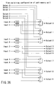
- FIG. 25 is a view explaining the recording data densities of the respective regions in the rewritable type information recording medium of this embodiment.
- the various dimensions of the system lead-in area of the reproduction-only information recording medium entirely coincide with those of the system lead-in area of the rewritable type information recording medium. Further, although not shown, in this embodiment, the various dimensions of the system lead-in area of the write-once type information recording medium coincide with the dimensions shown in FIG. 16 or FIG. 25.
- FIG. 26 shows the data structure of the lead-in area of the rewritable type information recording medium of this embodiment.
- embossed pits are formed in the system lead-in area shown, and rewritable recording marks are formed in the data lead-in area thereof.
- an initial zone includes an embossed data area.
- the main data of the data frame recorded in the initial zone is set to "00h".
- a buffer zone includes 32 ECC blocks (1024 sectors).
- the main data of the data frame recorded in the initial zone as a physical sector is set to "00h”.
- a control data zone includes an embossed data area.
- a data area includes emboss control data.
- connection area is used to connect the system lead-in area to the data lead-in area.
- the distance between the center line of the final sector "02 6BFFh" of the system lead-in area and the center line of the initial sector "02 6C00h” of the data lead-in area is set to 1.4 ⁇ m to 20.0 ⁇ m as an example.
- a physical sector number or a physical address is not allocated to the connection area, it does not include the physical sector number or the physical address.
- the data segment of a guard track zone does not include data.
- a disk test zone is used by a disk manufacturer to test quality.
- a drive test zone is used to execute a drive test.
- the information recording/reproducing apparatus optimizes recording conditions by writing trial data in this region.
- the disk ID zone in the data lead-in area includes drive information and a reserve area.
- the drive information is composed of the respective ECC blocks in a land truck and a groove track and starts from "02 CD00h” in the land track and starts from "82 CD00h” in the groove track.
- FIG. 28 shows the data structure of the lead-in area of the write-once type information recording medium of this embodiment.
- the write-once type information recording medium of this embodiment has a control data zone, which are common to the various types of the mediums, in a system lead-in area in which embossed pits are recorded. Further, the write-once type information recording medium has a disk test zone for trial write, and a drive test zone, a reference code zone, in which the reference signal for adjusting a reproduction circuit shown in FIG. 14 is recorded, a disk ID zone, and an R-physical format information zone in the data lead-in area thereof in which write-once type marks are recorded.
- the write-once type information recording medium of the embodiment is characterized in that a signal is detected in the system lead-in area using the level slice system and a signal is detected in the data lead-out area, the data area, and the data lead-out area using the PRML system.
- FIG. 29 shows a signal detection/signal evaluation circuit used to reproduce a signal in the system lead-in area.
- the outputs from quarter photo-detectors 13a to 13d are summed up, and the summed-up output is caused to pass through a high pass filter 122, and subjected to level slicing by a slicer 141 after the waveform thereof is corrected by a pre-equalizer 123.
- the circuit shown in FIG. 29 has the following circuit characteristics.
- PLL Phase lock loop
- the pre-equalizer is a seven-order equiripple filter and has a boot level k1 of 9.0 ⁇ 0.3 dB and a cut-off frequency of 16.5 ⁇ 0.5 MHz as frequency characteristics.
- circuit shown in FIG. 29 has the following circuit characteristics.
- a jitter is measured while a disk makes a quarter rotation in a frequency zone of from 1.0 KHz to HF.
- FIG. 30 is a circuit diagram showing a specific circuit used in the slicer shown in FIG. 29 that acts as a portion where the level slicing is executed.
- a signal output from the pre-equalizer (read channel 1) is binarized using a comparator.
- FIG. 31 shows a circuit diagram of a circuit for detecting the signal.
- the output from quarter photo-detectors are summed up, the summed-up output is caused to pass through a high pass filter 122, and the signal waveform of the summed-up output is used after the waveform is corrected by a pre-equalizer 123, similarly to the circuit arrangement shown in FIG. 29.
- a circuit before the output is supplied to a PRML circuit is characterized in that the amplitude of a reproduced signal is controlled to a given level using an automatic gain control (AGC) circuit 124.
- AGC automatic gain control
- the analog signal is converted into a digital signal by an analog to digital converter (ADC) circuit.
- ADC analog to digital converter
- PLL Phase lock loop
- the pre-equalizer is a seven-order equiripple filter and has a boot level k1 of 9.0 ⁇ 0.3 dB and a cut-off frequency of 16.5 ⁇ 0.5 MHz as frequency characteristics.
- a 9-tap transversal filter is used as an equalizer.
- a coefficient is controlled by a tap controller.
- the tap coefficient of the equalizer is calculated by a minimum square error (MSE) algorithm. An initial value is used as the tap coefficient before it is calculated.
- MSE minimum square error
- FIG. 32 shows the structure of a Viterbi decoder 128 used in the signal evaluation circuit shown in FIG. 31.
- PR(1,2,2,2,1) is employed as a PR class.
- the read channels from the data lead-in area, the data area, and the data lead-out area are combined with an ETM code so as to be in conformity with a PR(1,2,2,2,1) channel.
- FIG. 33 shows the transition of state of the PR channel.
- Sabcd shows that a previous 4-bit input is abcd, and e/f shows that next input data is e and a signal level is f.
- the Viterbi decoder outputs binary data from an equivalent signal as shown below.
- a branch metric at a time t is calculated as shown below.
- the resolution of the branch metric is equal to or larger than 10 bits.
- the path metric at time t is calculated as shown below.
- the resolution of the path metric is equal to or larger than 11 bits.
- An add-compare-select block (that corresponds to the ML decoder shown in FIG. 7) calculates a new path metric, supplies the new path metric to a path metric memory, and supplies a selection to a path memory.
- FIG. 34 shows an example of the path memory.
- the path memory has, for example, 20 memory cells.
- FIG. 35 shows the arrangements of an I/O and a path memory cell. As shown in FIG. 36, a final path memory cell outputs only one signal as binary data from an output 0.
- a signal can be reproduced by the level slice system until the level of double refraction reaches a predetermined magnitude in any type of optical discs, that is, any of the reproduction-only optical disk, the only-once-recordable (write-once type) optical disk, and the recording/reproducing optical disk (RAM disk), and, in the optical disk, which includes double refraction that has such a level as to reduce signal intensity when a signal is reproduced by the level slice system, the signal can be reproduced using the PRML system within the range of an appropriate error rate that is one rank higher than that in the level slice system. Further, it is admitted that a margin is increased with respect to a decrease in the signal intensity by employing the PRML system.
- the level of the double refraction included in respective types of the optical discs when the level permits a reproduced signal to be obtained within the range of a predetermined error rate, the level is set to:
Landscapes
- Engineering & Computer Science (AREA)
- Manufacturing & Machinery (AREA)
- Optical Recording Or Reproduction (AREA)
- Optical Record Carriers And Manufacture Thereof (AREA)
Applications Claiming Priority (2)
| Application Number | Priority Date | Filing Date | Title |
|---|---|---|---|
| JP2003102153 | 2003-04-04 | ||
| JP2003102153A JP2004310887A (ja) | 2003-04-04 | 2003-04-04 | 光ディスクならびに光ディスク装置 |
Publications (3)
| Publication Number | Publication Date |
|---|---|
| EP1465172A2 true EP1465172A2 (de) | 2004-10-06 |
| EP1465172A8 EP1465172A8 (de) | 2005-03-30 |
| EP1465172A3 EP1465172A3 (de) | 2006-05-31 |
Family
ID=32844724
Family Applications (1)
| Application Number | Title | Priority Date | Filing Date |
|---|---|---|---|
| EP04005001A Withdrawn EP1465172A3 (de) | 2003-04-04 | 2004-03-03 | Optische Platte und optisches Plattengerät |
Country Status (6)
| Country | Link |
|---|---|
| US (1) | US7408869B2 (de) |
| EP (1) | EP1465172A3 (de) |
| JP (1) | JP2004310887A (de) |
| KR (1) | KR100603231B1 (de) |
| CN (1) | CN1542757A (de) |
| TW (1) | TW200423087A (de) |
Cited By (5)
| Publication number | Priority date | Publication date | Assignee | Title |
|---|---|---|---|---|
| WO2006075700A1 (ja) | 2005-01-14 | 2006-07-20 | Pioneer Corporation | 記録媒体、記録装置及び記録方法、並びにコンピュータプログラム |
| EP1797555A1 (de) * | 2004-10-08 | 2007-06-20 | Samsung Electronics Co., Ltd. | Optisches aufzeichnungsmedium, aufzeichnungs-/wiedergabeverfahren und aufzeichnungs-/wiedergabevorrichtung |
| EP2109103A1 (de) * | 2008-04-11 | 2009-10-14 | Hitachi, Ltd. | Mehrschichtiges optisches Aufzeichnungsmedium |
| EP2256731A3 (de) * | 2005-04-14 | 2011-03-09 | Kabushiki Kaisha Toshiba | Speichermedium, Wiedergabeverfahren und Aufzeichnungsverfahren |
| EP2469532A3 (de) * | 2005-07-29 | 2012-12-05 | Kabushiki Kaisha Toshiba | Optischer Kopf und Informationsaufzeichnungs-/Informationswiedergabevorrichtung |
Families Citing this family (66)
| Publication number | Priority date | Publication date | Assignee | Title |
|---|---|---|---|---|
| JP2004327013A (ja) * | 2003-04-11 | 2004-11-18 | Nec Corp | 光ディスク媒体および光ディスク装置 |
| JP2005346769A (ja) * | 2004-05-31 | 2005-12-15 | Toshiba Corp | 光記録媒体及び情報記録再生装置 |
| US20090290476A1 (en) * | 2004-12-06 | 2009-11-26 | Mitsuya Okada | Optical information recording medium, optical information recording/reproducing apparatus, and method of manufacturing optical information recording medium |
| JP4390207B2 (ja) * | 2004-12-17 | 2009-12-24 | パイオニア株式会社 | オフセット量測定方法及び装置 |
| TWI259447B (en) * | 2005-01-11 | 2006-08-01 | Lite On It Corp | Optical reproducing/recording apparatus and method for detecting RF signal quality executed thereby |
| JP4660217B2 (ja) | 2005-01-31 | 2011-03-30 | 株式会社東芝 | 記憶媒体、再生方法、記録方法、再生装置及び記録装置 |
| JP2006236420A (ja) * | 2005-02-22 | 2006-09-07 | Toshiba Corp | 記憶媒体、再生方法及び記録方法 |
| JP2006236421A (ja) | 2005-02-22 | 2006-09-07 | Toshiba Corp | 記憶媒体、再生方法及び記録方法 |
| JP4080489B2 (ja) * | 2005-02-25 | 2008-04-23 | シャープ株式会社 | 記録条件設定装置、記録再生装置、記録条件設定方法、制御プログラム及び記録媒体 |
| US7804750B2 (en) * | 2005-11-09 | 2010-09-28 | Sanyo Electric Co., Ltd. | Test disc and drive verification method |
| JP2007234204A (ja) * | 2006-01-31 | 2007-09-13 | Toshiba Corp | 情報記憶媒体、情報記録方法および情報記録装置 |
| CN101385084A (zh) * | 2006-02-14 | 2009-03-11 | 皇家飞利浦电子股份有限公司 | 用于光盘读取的比特检测 |
| KR20080040896A (ko) * | 2006-11-06 | 2008-05-09 | 삼성전자주식회사 | 정보 저장 매체, 기록/재생 방법 및 장치 |
| US20080117791A1 (en) * | 2006-11-20 | 2008-05-22 | Atmel Corporation | Optical media identifications |
| MX2009010888A (es) * | 2007-12-11 | 2010-01-20 | Panasonic Corp | Medio de grabacion de informacion y metodo de evaluacion de medios de grabacion de informacion. |
| JP2011515018A (ja) * | 2008-02-12 | 2011-05-12 | クォルコム・メムズ・テクノロジーズ・インコーポレーテッド | 2層式薄膜ホログラフィック太陽光コレクタ及び太陽光コンセントレータ |
| JP2009283130A (ja) * | 2009-08-31 | 2009-12-03 | Toshiba Corp | 記憶媒体、再生方法及び記録方法 |
| JP2010262734A (ja) * | 2010-07-23 | 2010-11-18 | Toshiba Corp | 記憶媒体、再生方法及び記録方法 |
| JP2010267378A (ja) * | 2010-07-29 | 2010-11-25 | Toshiba Corp | 情報記憶媒体、再生方法、記録方法及び再生装置 |
| JP2010267377A (ja) * | 2010-07-29 | 2010-11-25 | Toshiba Corp | 情報記憶媒体、再生方法、記録方法及び再生装置 |
| JP2011070766A (ja) * | 2010-11-29 | 2011-04-07 | Toshiba Corp | 記憶媒体、再生方法、記録方法及び再生装置 |
| JP2011070765A (ja) * | 2010-11-29 | 2011-04-07 | Toshiba Corp | 記憶媒体、再生方法、記録方法、再生装置及び記録装置 |
| JP5106654B2 (ja) * | 2011-04-28 | 2012-12-26 | 株式会社東芝 | 記憶媒体、再生方法及び記録方法 |
| JP2011243283A (ja) * | 2011-09-05 | 2011-12-01 | Toshiba Corp | 情報記憶媒体、情報再生方法、情報再生装置、情報記録方法及び情報記録装置 |
| JP2012009133A (ja) * | 2011-09-05 | 2012-01-12 | Toshiba Corp | 情報記憶媒体、情報再生方法、情報再生装置、情報記録方法及び情報記録装置 |
| JP5060645B2 (ja) * | 2011-09-09 | 2012-10-31 | 株式会社東芝 | 記憶媒体、再生方法、記録方法、再生装置及び記録装置 |
| JP5060644B2 (ja) * | 2011-09-09 | 2012-10-31 | 株式会社東芝 | 記憶媒体、再生方法、記録方法、再生装置及び記録装置 |
| JP5060646B2 (ja) * | 2011-09-09 | 2012-10-31 | 株式会社東芝 | 記憶媒体、再生方法、記録方法、再生装置及び記録装置 |
| JP2012128945A (ja) * | 2012-04-02 | 2012-07-05 | Toshiba Corp | 記憶媒体、再生方法及び記録方法 |
| JP2012226823A (ja) * | 2012-07-09 | 2012-11-15 | Toshiba Corp | 情報記憶媒体、再生方法、再生装置、記録方法及び記録装置 |
| JP5166633B2 (ja) * | 2012-09-07 | 2013-03-21 | 株式会社東芝 | 記憶媒体、再生方法、記録方法、再生装置及び記録装置 |
| JP5173060B2 (ja) * | 2012-09-11 | 2013-03-27 | 株式会社東芝 | 記憶媒体、再生方法、記録方法、再生装置及び記録装置 |
| JP5173062B2 (ja) * | 2012-09-11 | 2013-03-27 | 株式会社東芝 | 記憶媒体、再生方法、記録方法、再生装置及び記録装置 |
| JP5173068B2 (ja) * | 2012-09-11 | 2013-03-27 | 株式会社東芝 | 記憶媒体、再生方法、記録方法、再生装置及び記録装置 |
| JP5173059B2 (ja) * | 2012-09-11 | 2013-03-27 | 株式会社東芝 | 記憶媒体、再生方法、記録方法、再生装置及び記録装置 |
| JP5173064B2 (ja) * | 2012-09-11 | 2013-03-27 | 株式会社東芝 | 記憶媒体、再生方法、記録方法、再生装置及び記録装置 |
| JP5173065B2 (ja) * | 2012-09-11 | 2013-03-27 | 株式会社東芝 | 記憶媒体、再生方法、記録方法、再生装置及び記録装置 |
| JP5173063B2 (ja) * | 2012-09-11 | 2013-03-27 | 株式会社東芝 | 記憶媒体、再生方法、記録方法、再生装置及び記録装置 |
| JP5173061B2 (ja) * | 2012-09-11 | 2013-03-27 | 株式会社東芝 | 記憶媒体、再生方法、記録方法、再生装置及び記録装置 |
| JP5173067B2 (ja) * | 2012-09-11 | 2013-03-27 | 株式会社東芝 | 記憶媒体、再生方法、記録方法、再生装置及び記録装置 |
| JP5173066B2 (ja) * | 2012-09-11 | 2013-03-27 | 株式会社東芝 | 記憶媒体、再生方法、記録方法、再生装置及び記録装置 |
| JP5166644B2 (ja) * | 2012-09-12 | 2013-03-21 | 株式会社東芝 | 記憶媒体、再生方法、記録方法、再生装置及び記録装置 |
| JP5166635B2 (ja) * | 2012-09-12 | 2013-03-21 | 株式会社東芝 | 記憶媒体、再生方法、記録方法、再生装置及び記録装置 |
| JP5173073B2 (ja) * | 2012-09-12 | 2013-03-27 | 株式会社東芝 | 記憶媒体、再生方法、記録方法、再生装置及び記録装置 |
| JP5166645B2 (ja) * | 2012-09-12 | 2013-03-21 | 株式会社東芝 | 記憶媒体、再生方法、記録方法、再生装置及び記録装置 |
| JP5166643B2 (ja) * | 2012-09-12 | 2013-03-21 | 株式会社東芝 | 記憶媒体、再生方法、記録方法、再生装置及び記録装置 |
| JP5166640B2 (ja) * | 2012-09-12 | 2013-03-21 | 株式会社東芝 | 記憶媒体、再生方法、記録方法、再生装置及び記録装置 |
| JP5173072B2 (ja) * | 2012-09-12 | 2013-03-27 | 株式会社東芝 | 記憶媒体、再生方法、記録方法、再生装置及び記録装置 |
| JP5166639B2 (ja) * | 2012-09-12 | 2013-03-21 | 株式会社東芝 | 記憶媒体、再生方法、記録方法、再生装置及び記録装置 |
| JP5166646B2 (ja) * | 2012-09-12 | 2013-03-21 | 株式会社東芝 | 記憶媒体、再生方法、記録方法、再生装置及び記録装置 |
| JP5173071B2 (ja) * | 2012-09-12 | 2013-03-27 | 株式会社東芝 | 記憶媒体、再生方法、記録方法、再生装置及び記録装置 |
| JP5173070B2 (ja) * | 2012-09-12 | 2013-03-27 | 株式会社東芝 | 記憶媒体、再生方法、記録方法、再生装置及び記録装置 |
| JP5166637B2 (ja) * | 2012-09-12 | 2013-03-21 | 株式会社東芝 | 記憶媒体、再生方法、記録方法、再生装置及び記録装置 |
| JP5173069B2 (ja) * | 2012-09-12 | 2013-03-27 | 株式会社東芝 | 記憶媒体、再生方法、記録方法、再生装置及び記録装置 |
| JP5166636B2 (ja) * | 2012-09-12 | 2013-03-21 | 株式会社東芝 | 記憶媒体、再生方法、記録方法、再生装置及び記録装置 |
| JP5166638B2 (ja) * | 2012-09-12 | 2013-03-21 | 株式会社東芝 | 記憶媒体、再生方法、記録方法、再生装置及び記録装置 |
| JP5166634B2 (ja) * | 2012-09-12 | 2013-03-21 | 株式会社東芝 | 記憶媒体、再生方法、記録方法、再生装置及び記録装置 |
| JP5173074B2 (ja) * | 2012-09-12 | 2013-03-27 | 株式会社東芝 | 記憶媒体、再生方法、記録方法、再生装置及び記録装置 |
| JP5166641B2 (ja) * | 2012-09-12 | 2013-03-21 | 株式会社東芝 | 記憶媒体、再生方法、記録方法、再生装置及び記録装置 |
| JP5166642B2 (ja) * | 2012-09-12 | 2013-03-21 | 株式会社東芝 | 記憶媒体、再生方法、記録方法、再生装置及び記録装置 |
| JP5166647B2 (ja) * | 2012-10-22 | 2013-03-21 | 株式会社東芝 | 記憶媒体、再生方法、記録方法、再生装置及び記録装置 |
| JP5619121B2 (ja) * | 2012-12-13 | 2014-11-05 | 株式会社東芝 | 記憶媒体、再生方法、記録方法、再生装置及び記録装置 |
| JP2013069406A (ja) * | 2012-12-13 | 2013-04-18 | Toshiba Corp | 記憶媒体、再生方法、再生装置、記録方法及び記録装置 |
| JP5619237B2 (ja) * | 2013-08-12 | 2014-11-05 | 株式会社東芝 | 記憶媒体、再生方法、記録方法、再生装置及び記録装置 |
| JP2014112458A (ja) * | 2014-01-20 | 2014-06-19 | Toshiba Corp | 情報記憶媒体、情報再生方法、情報再生装置、情報記録方法及び情報記録装置 |
| JP2014099242A (ja) * | 2014-02-28 | 2014-05-29 | Toshiba Corp | 記憶媒体、再生方法、記録方法、再生装置及び記録装置 |
Citations (8)
| Publication number | Priority date | Publication date | Assignee | Title |
|---|---|---|---|---|
| EP0395885A2 (de) * | 1989-03-31 | 1990-11-07 | The B.F. Goodrich Company | Substrat für optische Aufzeichnungsmedien und Formmasse dafür |
| US4990386A (en) * | 1987-12-22 | 1991-02-05 | Showa Denko Kabushiki Kaishi | Optical disk substrate |
| US5176859A (en) * | 1989-12-08 | 1993-01-05 | Philips And Du Pont Optical Company | Apparatus/and method for controlling an injection molding process producing a molded part |
| EP0794209A2 (de) * | 1996-03-07 | 1997-09-10 | Idemitsu Petrochemical Co., Ltd. | Endgruppenmodifizierte Polycarbonate für digitale Bildplatten |
| WO2001016950A1 (en) * | 1999-08-27 | 2001-03-08 | The Dow Chemical Company | High data density optical media discs |
| EP1193274A1 (de) * | 1998-12-04 | 2002-04-03 | Nippon Zeon Co., Ltd. | Hydrierte polymere, harzzusammensetzung und verfahren zur herstellung von einem substrat zur verwendung als datenaufzeichnungsträger |
| US6436503B1 (en) * | 1999-09-08 | 2002-08-20 | General Electric Company | Data storage medium containing polyestercarbonate |
| US6537636B1 (en) * | 2000-06-05 | 2003-03-25 | General Electric Company | Data storage media containing clear polycarbonate blends |
Family Cites Families (12)
| Publication number | Priority date | Publication date | Assignee | Title |
|---|---|---|---|---|
| JP3351164B2 (ja) | 1995-03-24 | 2002-11-25 | 日本ビクター株式会社 | 光学的情報記録媒体の製造方法 |
| US6207247B1 (en) * | 1998-03-27 | 2001-03-27 | Nikon Corporation | Method for manufacturing a molding tool used for sustrate molding |
| JP2000067468A (ja) | 1998-08-25 | 2000-03-03 | Teijin Ltd | 光ディスクおよびその製造方法 |
| JP2000099997A (ja) * | 1998-09-22 | 2000-04-07 | Toshiba Corp | 光ディスクおよび光ディスク装置 |
| JP2000322767A (ja) | 1999-05-10 | 2000-11-24 | Victor Co Of Japan Ltd | 光ディスク |
| JP2001126311A (ja) | 1999-10-26 | 2001-05-11 | Jsr Corp | 光学用成形材料および光ディスク |
| US7133331B2 (en) * | 2000-12-28 | 2006-11-07 | Victor Company Of Japan, Limited | Recording medium having a substrate containing microscopic pattern of parallel groove and land sections and recording/reproducing equipment therefor |
| JP2002304770A (ja) | 2001-02-01 | 2002-10-18 | Victor Co Of Japan Ltd | 光ディスク |
| JP2002237096A (ja) * | 2001-02-09 | 2002-08-23 | Ricoh Co Ltd | 光記録媒体 |
| JP2003022580A (ja) * | 2001-05-02 | 2003-01-24 | Victor Co Of Japan Ltd | 情報記録担体、情報記録担体の製造方法、情報記録担体再生装置及び情報記録担体記録装置 |
| JP2004013947A (ja) * | 2002-06-04 | 2004-01-15 | Victor Co Of Japan Ltd | 情報記録担体、再生装置、記録装置、記録再生装置、再生方法、記録方法及び記録再生方法 |
| US7351516B2 (en) * | 2002-11-06 | 2008-04-01 | Ricoh Company, Ltd. | Optical information recording medium |
-
2003
- 2003-04-04 JP JP2003102153A patent/JP2004310887A/ja active Pending
-
2004
- 2004-03-03 EP EP04005001A patent/EP1465172A3/de not_active Withdrawn
- 2004-03-05 TW TW093105940A patent/TW200423087A/zh unknown
- 2004-03-18 US US10/803,057 patent/US7408869B2/en not_active Expired - Fee Related
- 2004-03-24 CN CNA200410031560XA patent/CN1542757A/zh active Pending
- 2004-03-25 KR KR1020040020428A patent/KR100603231B1/ko not_active IP Right Cessation
Patent Citations (8)
| Publication number | Priority date | Publication date | Assignee | Title |
|---|---|---|---|---|
| US4990386A (en) * | 1987-12-22 | 1991-02-05 | Showa Denko Kabushiki Kaishi | Optical disk substrate |
| EP0395885A2 (de) * | 1989-03-31 | 1990-11-07 | The B.F. Goodrich Company | Substrat für optische Aufzeichnungsmedien und Formmasse dafür |
| US5176859A (en) * | 1989-12-08 | 1993-01-05 | Philips And Du Pont Optical Company | Apparatus/and method for controlling an injection molding process producing a molded part |
| EP0794209A2 (de) * | 1996-03-07 | 1997-09-10 | Idemitsu Petrochemical Co., Ltd. | Endgruppenmodifizierte Polycarbonate für digitale Bildplatten |
| EP1193274A1 (de) * | 1998-12-04 | 2002-04-03 | Nippon Zeon Co., Ltd. | Hydrierte polymere, harzzusammensetzung und verfahren zur herstellung von einem substrat zur verwendung als datenaufzeichnungsträger |
| WO2001016950A1 (en) * | 1999-08-27 | 2001-03-08 | The Dow Chemical Company | High data density optical media discs |
| US6436503B1 (en) * | 1999-09-08 | 2002-08-20 | General Electric Company | Data storage medium containing polyestercarbonate |
| US6537636B1 (en) * | 2000-06-05 | 2003-03-25 | General Electric Company | Data storage media containing clear polycarbonate blends |
Cited By (26)
| Publication number | Priority date | Publication date | Assignee | Title |
|---|---|---|---|---|
| EP1797555A1 (de) * | 2004-10-08 | 2007-06-20 | Samsung Electronics Co., Ltd. | Optisches aufzeichnungsmedium, aufzeichnungs-/wiedergabeverfahren und aufzeichnungs-/wiedergabevorrichtung |
| EP1797555A4 (de) * | 2004-10-08 | 2008-09-03 | Samsung Electronics Co Ltd | Optisches aufzeichnungsmedium, aufzeichnungs-/wiedergabeverfahren und aufzeichnungs-/wiedergabevorrichtung |
| US7957245B2 (en) | 2005-01-14 | 2011-06-07 | Pioneer Corporation | Recording medium, recording method, and computer program |
| EP1837873A1 (de) * | 2005-01-14 | 2007-09-26 | Pioneer Corporation | Aufzeichnungsmedium, aufzeichnungsvorrichtung, aufzeichnungsverfahren und computerprogramm |
| EP1837873A4 (de) * | 2005-01-14 | 2009-07-01 | Pioneer Corp | Aufzeichnungsmedium, aufzeichnungsvorrichtung, aufzeichnungsverfahren und computerprogramm |
| WO2006075700A1 (ja) | 2005-01-14 | 2006-07-20 | Pioneer Corporation | 記録媒体、記録装置及び記録方法、並びにコンピュータプログラム |
| US8142981B2 (en) | 2005-04-14 | 2012-03-27 | Kabushiki Kaisha Toshiba | Storage medium, reproducing method, and recording method |
| US8325584B2 (en) | 2005-04-14 | 2012-12-04 | Kabushiki Kaisha Toshiba | Storage medium, reproducing method, and recording method |
| EP2256730A3 (de) * | 2005-04-14 | 2011-03-16 | Kabushiki Kaisha Toshiba | Speichermedium, Wiedergabeverfahren und Aufzeichnungsverfahren |
| EP2259259A3 (de) * | 2005-04-14 | 2011-03-23 | Kabushiki Kaisha Toshiba | Speichermedium, Wiedergabeverfahren und Aufzeichnungsverfahren |
| EP2273499A3 (de) * | 2005-04-14 | 2011-03-30 | Kabushiki Kaisha Toshiba | Speichermedium, Wiedergabeverfahren und Aufzeichnungsverfahren |
| EP2256731A3 (de) * | 2005-04-14 | 2011-03-09 | Kabushiki Kaisha Toshiba | Speichermedium, Wiedergabeverfahren und Aufzeichnungsverfahren |
| US8588047B2 (en) | 2005-04-14 | 2013-11-19 | Kabushiki Kaisha Toshiba | Storage medium, reproducing method, and recording method |
| US8252510B2 (en) | 2005-04-14 | 2012-08-28 | Kabushiki Kaisha Toshiba | Storage medium, reproducing method, and recording method |
| US8374069B2 (en) | 2005-04-14 | 2013-02-12 | Kabushiki Kaisha Toshiba | Storage medium, reproducing method, and recording method |
| EP2254114A3 (de) * | 2005-04-14 | 2011-03-09 | Kabushiki Kaisha Toshiba | Speichermedium, Wiedergabeverfahren und Aufzeichnungsverfahren |
| EP2469532A3 (de) * | 2005-07-29 | 2012-12-05 | Kabushiki Kaisha Toshiba | Optischer Kopf und Informationsaufzeichnungs-/Informationswiedergabevorrichtung |
| EP2469531A3 (de) * | 2005-07-29 | 2012-12-05 | Kabushiki Kaisha Toshiba | Optischer Kopf und Informationsaufzeichnungs-/Informationswiedergabevorrichtung |
| EP2469516A3 (de) * | 2005-07-29 | 2012-12-05 | Kabushiki Kaisha Toshiba | Optischer Kopf und Informationsaufzeichnungs-/Informationswiedergabevorrichtung |
| EP2469518A3 (de) * | 2005-07-29 | 2012-12-12 | Kabushiki Kaisha Toshiba | Optischer Kopf und Informationsaufzeichnungs-/Informationswiedergabevorrichtung |
| EP2469533A3 (de) * | 2005-07-29 | 2012-12-12 | Kabushiki Kaisha Toshiba | Optischer Kopf und Informationsaufzeichnungs-/Informationswiedergabevorrichtung |
| EP2469534A3 (de) * | 2005-07-29 | 2012-12-12 | Kabushiki Kaisha Toshiba | Optischer Kopf und Informationsaufzeichnungs-/Informationswiedergabevorrichtung |
| EP2469517A3 (de) * | 2005-07-29 | 2012-12-12 | Kabushiki Kaisha Toshiba | Optischer Kopf und Informationsaufzeichnungs-/Informationswiedergabevorrichtung |
| US8717858B2 (en) | 2005-07-29 | 2014-05-06 | Kabushiki Kaisha Toshiba | Write-once type information storage medium (disk structure of recording type information storage medium having structure in which recording layer formed on transparent susbstrate is defined as inside), and information reproducing method or information recording method as well as storage medium manufacturing |
| US8315147B2 (en) | 2008-04-11 | 2012-11-20 | Hitachi, Ltd. | Multilayer optical recording medium having three or more recording layers with reduced interlayer crosstalk |
| EP2109103A1 (de) * | 2008-04-11 | 2009-10-14 | Hitachi, Ltd. | Mehrschichtiges optisches Aufzeichnungsmedium |
Also Published As
| Publication number | Publication date |
|---|---|
| JP2004310887A (ja) | 2004-11-04 |
| TW200423087A (en) | 2004-11-01 |
| EP1465172A8 (de) | 2005-03-30 |
| US7408869B2 (en) | 2008-08-05 |
| US20040196776A1 (en) | 2004-10-07 |
| CN1542757A (zh) | 2004-11-03 |
| KR100603231B1 (ko) | 2006-07-24 |
| KR20040086746A (ko) | 2004-10-12 |
| EP1465172A3 (de) | 2006-05-31 |
Similar Documents
| Publication | Publication Date | Title |
|---|---|---|
| US7408869B2 (en) | Optical disk and optical disk apparatus | |
| CA2384263C (en) | Optical disc having uniform structure | |
| US7616543B2 (en) | Disk recording medium, disk drive apparatus, reproducing method, and disk manufacturing method | |
| KR20060042900A (ko) | 기록 매체 평가 방법, 기록 재생 장치, 및 기록 매체 | |
| KR100557723B1 (ko) | 정보 기억 매체 평가 방법, 정보 기억 매체 평가 장치,정보 기억 매체, 정보 재생 장치, 정보 재생 방법 및 정보기록 방법 | |
| JP2004296050A (ja) | 光ディスクならびに光ディスク装置 | |
| JP2006338876A (ja) | 光ディスクならびに光ディスク装置 | |
| JP5191198B2 (ja) | 光記録媒体、光記録再生システム | |
| JP2007510244A (ja) | 修正されたcd層を持つハイブリッド光学情報記録媒体 | |
| Richter et al. | Present and future applications of phase-change recording technology | |
| JP2005078697A (ja) | 光記録媒体、その駆動装置およびその再生方法 | |
| JP2009123278A (ja) | 光記録媒体 |
Legal Events
| Date | Code | Title | Description |
|---|---|---|---|
| PUAI | Public reference made under article 153(3) epc to a published international application that has entered the european phase |
Free format text: ORIGINAL CODE: 0009012 |
|
| 17P | Request for examination filed |
Effective date: 20040303 |
|
| AK | Designated contracting states |
Kind code of ref document: A2 Designated state(s): AT BE BG CH CY CZ DE DK EE ES FI FR GB GR HU IE IT LI LU MC NL PL PT RO SE SI SK TR |
|
| AX | Request for extension of the european patent |
Extension state: AL LT LV MK |
|
| RIN1 | Information on inventor provided before grant (corrected) |
Inventor name: TAKAZAWA, KOJI Inventor name: YOSHIDA, NOBUHISA |
|
| RIN1 | Information on inventor provided before grant (corrected) |
Inventor name: TAKAZAWA, KOJI Inventor name: YOSHIDA, NOBUHISA |
|
| RIN1 | Information on inventor provided before grant (corrected) |
Inventor name: TAKAZAWA, KOJI,C/O TOSHIBA CORPORATION Inventor name: YOSHIDA, NOBUHISA,C/O TOSHIBA CORPORATION |
|
| PUAL | Search report despatched |
Free format text: ORIGINAL CODE: 0009013 |
|
| AK | Designated contracting states |
Kind code of ref document: A3 Designated state(s): AT BE BG CH CY CZ DE DK EE ES FI FR GB GR HU IE IT LI LU MC NL PL PT RO SE SI SK TR |
|
| AX | Request for extension of the european patent |
Extension state: AL LT LV MK |
|
| RIC1 | Information provided on ipc code assigned before grant |
Ipc: G11B 7/253 20060101ALI20060407BHEP Ipc: G11B 7/00 20060101ALI20060407BHEP Ipc: G11B 7/24 20060101AFI20060407BHEP |
|
| 17Q | First examination report despatched |
Effective date: 20060816 |
|
| AKX | Designation fees paid |
Designated state(s): DE FR GB |
|
| 17Q | First examination report despatched |
Effective date: 20060816 |
|
| STAA | Information on the status of an ep patent application or granted ep patent |
Free format text: STATUS: THE APPLICATION IS DEEMED TO BE WITHDRAWN |
|
| 18D | Application deemed to be withdrawn |
Effective date: 20081115 |