EP1458022A2 - Halbleiteranordnung, Herstellungsverfahren dafür, Halbleiter-Substrat, Leiterplatte, und elektronischer Apparat - Google Patents
Halbleiteranordnung, Herstellungsverfahren dafür, Halbleiter-Substrat, Leiterplatte, und elektronischer Apparat Download PDFInfo
- Publication number
- EP1458022A2 EP1458022A2 EP04001891A EP04001891A EP1458022A2 EP 1458022 A2 EP1458022 A2 EP 1458022A2 EP 04001891 A EP04001891 A EP 04001891A EP 04001891 A EP04001891 A EP 04001891A EP 1458022 A2 EP1458022 A2 EP 1458022A2
- Authority
- EP
- European Patent Office
- Prior art keywords
- resin layer
- recesses
- semiconductor device
- semiconductor
- interconnecting line
- Prior art date
- Legal status (The legal status is an assumption and is not a legal conclusion. Google has not performed a legal analysis and makes no representation as to the accuracy of the status listed.)
- Withdrawn
Links
Images

Classifications
-
- H—ELECTRICITY
- H10—SEMICONDUCTOR DEVICES; ELECTRIC SOLID-STATE DEVICES NOT OTHERWISE PROVIDED FOR
- H10W—GENERIC PACKAGES, INTERCONNECTIONS, CONNECTORS OR OTHER CONSTRUCTIONAL DETAILS OF DEVICES COVERED BY CLASS H10
- H10W72/00—Interconnections or connectors in packages
- H10W72/20—Bump connectors, e.g. solder bumps or copper pillars; Dummy bumps; Thermal bumps
-
- E—FIXED CONSTRUCTIONS
- E06—DOORS, WINDOWS, SHUTTERS, OR ROLLER BLINDS IN GENERAL; LADDERS
- E06B—FIXED OR MOVABLE CLOSURES FOR OPENINGS IN BUILDINGS, VEHICLES, FENCES OR LIKE ENCLOSURES IN GENERAL, e.g. DOORS, WINDOWS, BLINDS, GATES
- E06B9/00—Screening or protective devices for wall or similar openings, with or without operating or securing mechanisms; Closures of similar construction
- E06B9/24—Screens or other constructions affording protection against light, especially against sunshine; Similar screens for privacy or appearance; Slat blinds
- E06B9/26—Lamellar or like blinds, e.g. venetian blinds
- E06B9/28—Lamellar or like blinds, e.g. venetian blinds with horizontal lamellae, e.g. non-liftable
- E06B9/30—Lamellar or like blinds, e.g. venetian blinds with horizontal lamellae, e.g. non-liftable liftable
- E06B9/32—Operating, guiding, or securing devices therefor
- E06B9/322—Details of operating devices, e.g. pulleys, brakes, spring drums, drives
-
- E—FIXED CONSTRUCTIONS
- E06—DOORS, WINDOWS, SHUTTERS, OR ROLLER BLINDS IN GENERAL; LADDERS
- E06B—FIXED OR MOVABLE CLOSURES FOR OPENINGS IN BUILDINGS, VEHICLES, FENCES OR LIKE ENCLOSURES IN GENERAL, e.g. DOORS, WINDOWS, BLINDS, GATES
- E06B9/00—Screening or protective devices for wall or similar openings, with or without operating or securing mechanisms; Closures of similar construction
- E06B9/24—Screens or other constructions affording protection against light, especially against sunshine; Similar screens for privacy or appearance; Slat blinds
- E06B9/26—Lamellar or like blinds, e.g. venetian blinds
- E06B9/28—Lamellar or like blinds, e.g. venetian blinds with horizontal lamellae, e.g. non-liftable
- E06B9/30—Lamellar or like blinds, e.g. venetian blinds with horizontal lamellae, e.g. non-liftable liftable
- E06B9/303—Lamellar or like blinds, e.g. venetian blinds with horizontal lamellae, e.g. non-liftable liftable with ladder-tape
- E06B9/307—Details of tilting bars and their operation
-
- H—ELECTRICITY
- H10—SEMICONDUCTOR DEVICES; ELECTRIC SOLID-STATE DEVICES NOT OTHERWISE PROVIDED FOR
- H10P—GENERIC PROCESSES OR APPARATUS FOR THE MANUFACTURE OR TREATMENT OF DEVICES COVERED BY CLASS H10
- H10P54/00—Cutting or separating of wafers, substrates or parts of devices
-
- H—ELECTRICITY
- H10—SEMICONDUCTOR DEVICES; ELECTRIC SOLID-STATE DEVICES NOT OTHERWISE PROVIDED FOR
- H10W—GENERIC PACKAGES, INTERCONNECTIONS, CONNECTORS OR OTHER CONSTRUCTIONAL DETAILS OF DEVICES COVERED BY CLASS H10
- H10W72/00—Interconnections or connectors in packages
- H10W72/01—Manufacture or treatment
- H10W72/012—Manufacture or treatment of bump connectors, dummy bumps or thermal bumps
-
- H—ELECTRICITY
- H10—SEMICONDUCTOR DEVICES; ELECTRIC SOLID-STATE DEVICES NOT OTHERWISE PROVIDED FOR
- H10W—GENERIC PACKAGES, INTERCONNECTIONS, CONNECTORS OR OTHER CONSTRUCTIONAL DETAILS OF DEVICES COVERED BY CLASS H10
- H10W74/00—Encapsulations, e.g. protective coatings
- H10W74/10—Encapsulations, e.g. protective coatings characterised by their shape or disposition
- H10W74/111—Encapsulations, e.g. protective coatings characterised by their shape or disposition the semiconductor body being completely enclosed
- H10W74/129—Encapsulations, e.g. protective coatings characterised by their shape or disposition the semiconductor body being completely enclosed forming a chip-scale package [CSP]
-
- H—ELECTRICITY
- H10—SEMICONDUCTOR DEVICES; ELECTRIC SOLID-STATE DEVICES NOT OTHERWISE PROVIDED FOR
- H10W—GENERIC PACKAGES, INTERCONNECTIONS, CONNECTORS OR OTHER CONSTRUCTIONAL DETAILS OF DEVICES COVERED BY CLASS H10
- H10W74/00—Encapsulations, e.g. protective coatings
- H10W74/10—Encapsulations, e.g. protective coatings characterised by their shape or disposition
- H10W74/131—Encapsulations, e.g. protective coatings characterised by their shape or disposition the semiconductor body being only partially enclosed
- H10W74/147—Encapsulations, e.g. protective coatings characterised by their shape or disposition the semiconductor body being only partially enclosed the encapsulations being multilayered
-
- H—ELECTRICITY
- H10—SEMICONDUCTOR DEVICES; ELECTRIC SOLID-STATE DEVICES NOT OTHERWISE PROVIDED FOR
- H10W—GENERIC PACKAGES, INTERCONNECTIONS, CONNECTORS OR OTHER CONSTRUCTIONAL DETAILS OF DEVICES COVERED BY CLASS H10
- H10W70/00—Package substrates; Interposers; Redistribution layers [RDL]
- H10W70/01—Manufacture or treatment
- H10W70/05—Manufacture or treatment of insulating or insulated package substrates, or of interposers, or of redistribution layers
-
- H—ELECTRICITY
- H10—SEMICONDUCTOR DEVICES; ELECTRIC SOLID-STATE DEVICES NOT OTHERWISE PROVIDED FOR
- H10W—GENERIC PACKAGES, INTERCONNECTIONS, CONNECTORS OR OTHER CONSTRUCTIONAL DETAILS OF DEVICES COVERED BY CLASS H10
- H10W70/00—Package substrates; Interposers; Redistribution layers [RDL]
- H10W70/60—Insulating or insulated package substrates; Interposers; Redistribution layers
-
- H—ELECTRICITY
- H10—SEMICONDUCTOR DEVICES; ELECTRIC SOLID-STATE DEVICES NOT OTHERWISE PROVIDED FOR
- H10W—GENERIC PACKAGES, INTERCONNECTIONS, CONNECTORS OR OTHER CONSTRUCTIONAL DETAILS OF DEVICES COVERED BY CLASS H10
- H10W70/00—Package substrates; Interposers; Redistribution layers [RDL]
- H10W70/60—Insulating or insulated package substrates; Interposers; Redistribution layers
- H10W70/62—Insulating or insulated package substrates; Interposers; Redistribution layers characterised by their interconnections
- H10W70/65—Shapes or dispositions of interconnections
-
- H—ELECTRICITY
- H10—SEMICONDUCTOR DEVICES; ELECTRIC SOLID-STATE DEVICES NOT OTHERWISE PROVIDED FOR
- H10W—GENERIC PACKAGES, INTERCONNECTIONS, CONNECTORS OR OTHER CONSTRUCTIONAL DETAILS OF DEVICES COVERED BY CLASS H10
- H10W70/00—Package substrates; Interposers; Redistribution layers [RDL]
- H10W70/60—Insulating or insulated package substrates; Interposers; Redistribution layers
- H10W70/67—Insulating or insulated package substrates; Interposers; Redistribution layers characterised by their insulating layers or insulating parts
- H10W70/68—Shapes or dispositions thereof
-
- H—ELECTRICITY
- H10—SEMICONDUCTOR DEVICES; ELECTRIC SOLID-STATE DEVICES NOT OTHERWISE PROVIDED FOR
- H10W—GENERIC PACKAGES, INTERCONNECTIONS, CONNECTORS OR OTHER CONSTRUCTIONAL DETAILS OF DEVICES COVERED BY CLASS H10
- H10W72/00—Interconnections or connectors in packages
- H10W72/20—Bump connectors, e.g. solder bumps or copper pillars; Dummy bumps; Thermal bumps
- H10W72/241—Dispositions, e.g. layouts
- H10W72/242—Dispositions, e.g. layouts relative to the surface, e.g. recessed, protruding
-
- H—ELECTRICITY
- H10—SEMICONDUCTOR DEVICES; ELECTRIC SOLID-STATE DEVICES NOT OTHERWISE PROVIDED FOR
- H10W—GENERIC PACKAGES, INTERCONNECTIONS, CONNECTORS OR OTHER CONSTRUCTIONAL DETAILS OF DEVICES COVERED BY CLASS H10
- H10W72/00—Interconnections or connectors in packages
- H10W72/20—Bump connectors, e.g. solder bumps or copper pillars; Dummy bumps; Thermal bumps
- H10W72/241—Dispositions, e.g. layouts
- H10W72/244—Dispositions, e.g. layouts relative to underlying supporting features, e.g. bond pads, RDLs or vias
-
- H—ELECTRICITY
- H10—SEMICONDUCTOR DEVICES; ELECTRIC SOLID-STATE DEVICES NOT OTHERWISE PROVIDED FOR
- H10W—GENERIC PACKAGES, INTERCONNECTIONS, CONNECTORS OR OTHER CONSTRUCTIONAL DETAILS OF DEVICES COVERED BY CLASS H10
- H10W72/00—Interconnections or connectors in packages
- H10W72/20—Bump connectors, e.g. solder bumps or copper pillars; Dummy bumps; Thermal bumps
- H10W72/251—Materials
-
- H—ELECTRICITY
- H10—SEMICONDUCTOR DEVICES; ELECTRIC SOLID-STATE DEVICES NOT OTHERWISE PROVIDED FOR
- H10W—GENERIC PACKAGES, INTERCONNECTIONS, CONNECTORS OR OTHER CONSTRUCTIONAL DETAILS OF DEVICES COVERED BY CLASS H10
- H10W72/00—Interconnections or connectors in packages
- H10W72/20—Bump connectors, e.g. solder bumps or copper pillars; Dummy bumps; Thermal bumps
- H10W72/29—Bond pads specially adapted therefor
-
- H—ELECTRICITY
- H10—SEMICONDUCTOR DEVICES; ELECTRIC SOLID-STATE DEVICES NOT OTHERWISE PROVIDED FOR
- H10W—GENERIC PACKAGES, INTERCONNECTIONS, CONNECTORS OR OTHER CONSTRUCTIONAL DETAILS OF DEVICES COVERED BY CLASS H10
- H10W72/00—Interconnections or connectors in packages
- H10W72/90—Bond pads, in general
- H10W72/921—Structures or relative sizes of bond pads
- H10W72/922—Bond pads being integral with underlying chip-level interconnections
-
- H—ELECTRICITY
- H10—SEMICONDUCTOR DEVICES; ELECTRIC SOLID-STATE DEVICES NOT OTHERWISE PROVIDED FOR
- H10W—GENERIC PACKAGES, INTERCONNECTIONS, CONNECTORS OR OTHER CONSTRUCTIONAL DETAILS OF DEVICES COVERED BY CLASS H10
- H10W74/00—Encapsulations, e.g. protective coatings
- H10W74/10—Encapsulations, e.g. protective coatings characterised by their shape or disposition
- H10W74/111—Encapsulations, e.g. protective coatings characterised by their shape or disposition the semiconductor body being completely enclosed
- H10W74/127—Encapsulations, e.g. protective coatings characterised by their shape or disposition the semiconductor body being completely enclosed characterised by arrangements for sealing or adhesion
Definitions
- the present invention relates to a semiconductor device and method of manufacture thereof, and to a semiconductor wafer, circuit board, and electronic instrument.
- wafer level CSP Chip Scale/Size Package
- the present invention improves the reliability of a semiconductor device and method of manufacture thereof, a semiconductor wafer, a circuit board, and an electronic instrument.
- CSP Chip Size/Scale Package
- a semiconductor substrate for example, a semiconductor wafer
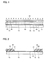
- an integrated circuit 12 On the semiconductor substrate 10 is formed an integrated circuit 12.
- the semiconductor substrate 10 is cut into a plurality of semiconductor chips 90 (see Fig. 7), a plurality of integrated circuits 12 is formed on the semiconductor substrate 10, and each semiconductor chip 90 has its own integrated circuit 12.
- a passivation film 14 of at least one layer may be formed on the surface of the semiconductor substrate 10.
- the passivation film 14 is an electrical insulating film.
- the passivation film 14 may be formed only of a material that is not a resin (for example, SiO2 or SiN), or may further include thereon a film formed of a resin (for example, polyimide resin).
- the passivation film 14 does not include conducting particles.
- the electrodes 16 may be parts (extremities) of interconnecting lines electrically connected to the integrated circuit 12.
- the passivation film 14 is formed to avoid at least a central portion of the electrodes 16.
- the passivation film 14 may overlap the extremities of the electrodes 16.
- a resin layer 20 is formed on the semiconductor substrate 10.
- the resin layer 20 may be formed by applying a resin precursor to the semiconductor substrate 10, or by spreading a resin precursor on the semiconductor substrate 10 by spin coating.
- the resin layer 20 includes both states of before and after curing (polymerization).
- the resin layer 20 may be a plurality of layers, or may be a single layer.
- the resin layer 20 is an electrical insulation layer.
- the resin layer 20 may have a stress relieving function after curing (polymerization).
- the resin layer 20 may be formed of a polyimide resin, a silicone denatured polyimide resin, an epoxy resin, a silicone denatured epoxy resin, benzocyclobutene (BCB), polybenzoxazole (PBO), or similar resins (or precursors thereof). resin layer 20 does not include conducting particles.
- the resin layer 20 may be formed of a material opaque to light.
- the resin layer 20 may be formed of a radiation-sensitive resin precursor, which has the property of being sensitive to radiation (light (ultraviolet radiation, visible light), X-rays, electron beam).
- Radiation-sensitive resin precursors for example, photosensitive resin precursors
- the resin layer 20 may be patterned. Patterning refers to the removal of a region of the resin layer 20 to form a penetrating space therein.
- lithography for example, photolithography
- a mask 30 is used.
- the mask 30 may have a transparent-and-opaque portion 32 for removing the portion of the resin layer 20 in the cutting region (for example, a scribing line) when the semiconductor substrate 10 is cut into a plurality of semiconductor chips 90 (see Fig. 7).
- the transparent-and-opaque portion 32 may be disposed so as to extend over the electrodes 16.
- the transparent-and-opaque portion 32 may be disposed so as to extend over the region to form the semiconductor chip.
- the transparent-and-opaque portion 32 is a portion transparent to energy (for example, light).
- the transparent-and-opaque portion 32 is a portion opaque to energy (for example, light).
- radiation also penetrates in the region directly below the transparent-and-opaque portion 32.
- the resin layer 20 may have a slanting surface 21 at the extremity formed by the patterning. The patterning of the resin layer 20 may be carried out so that the slanting surface 21 does not extend over the integrated circuit 12, or so that the slanting surface 21 does extend over the integrated circuit 12.
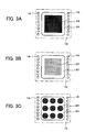
- the mask 30 may include in the resin layer 20 a transparent-and-opaque pattern 34 for carrying out energy irradiation (for example, light irradiation) with too fine pattern to be resolved.
- energy irradiation for example, light irradiation
- a " too fine pattern to be resolved” is meant a pattern so fine that a penetrating space cannot be formed in the resin layer 20.
- energy irradiation for example, light irradiation
- the transparent-and-opaque pattern 34 is for the purpose of forming recesses 22 in the resin layer 20, and is of a form (including a form of reversed sense) corresponding to the form of the recesses 22 (opening thereof).
- the transparent-and-opaque pattern 34 includes an opaque portion 36. Since the radiation is blocked by the opaque portion 36, the region of the resin layer 20 corresponding to the opaque portion 36 is not reduced in solubility.
- the opaque portion 36 is formed as a too fine form for the resin layer 20 to be resolved.
- the width of the opaque portion 36 may be not exceeding one-fourths of the thickness of the resin layer 20.
- the width of the opaque portion 36 may be not exceeding the thickness of the interconnecting lines formed on the resin layer 20, and may be less than this.
- a plurality of recesses 22 on the surface of the resin layer 20 is formed a plurality of recesses 22.
- lithography for example, photolithography
- the resin layer 20 is irradiated with energy through the transparent-and-opaque pattern 34, since the transparent-and-opaque pattern 34 has a too fine form for the resin layer 20 to be resolved, instead of penetrating spaces being formed in the resin layer 20, recesses 22 are formed.
- the recesses 22 have bottom surfaces. The bottom surface may be flat, and may be parallel to the surface in which opening of the recesses 22 is formed.
- the recesses 22 may be formed over the integrated circuit 12.
- the recesses 22 may be formed so as to widen from the bottom surface toward the outside. In this case, the inner wall surface of the recesses 22 may be tapered.
- the formation of the recesses 22 may be carried out at the same time as the patterning of the resin layer 20, or may be carried out separately.
- the recesses 22 are formed so that their opening width is less than the thickness of interconnecting lines 40 formed on the resin layer 20 (see Fig. 4A).
- the recesses 22 are formed to have a depth (for example, a depth of at least 1 ⁇ m) such as to improve the adhesion properties between the resin layer 20 and the interconnecting lines 40 formed thereon.
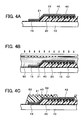
- Figs. 3A to 3C illustrate plan forms of the recess openings, and show the region of the semiconductor substrate 10 to form a single semiconductor chip.
- the plurality of recesses 24 shown in Fig. 3A forms an interconnected lattice.
- the plurality of recesses 26 shown in Fig. 3B is disposed in an isolating manner.
- the opening form of each recess 26 may be a quadrilateral, or may be a circle.
- Each recess 28 shown in Fig. 3C is in the form of a ring.
- a group of concentric recesses 28 may be formed at the position of formation of a land 42 (see Fig. 5A) of an interconnecting line 40 formed on the resin layer 20.
- a plurality of recesses may form a plurality of grooves.
- the transparent-and-opaque pattern 34 of the mask 30 has a form corresponding to the form of the opening of a recess (including a form of reversed sense).
- the resin layer 20 is developed. By means of development, the recesses 22 are formed.
- the resin layer 20 is formed of a negative type of radiation-sensitive resin precursor, the whole surface of the resin layer 20 in which the recesses 22 are formed may be irradiated with energy (for example, total exposure to light). By means of this, the whole of the resin layer 20 can be cured.
- the resin layer 20 in which the recesses 22 are formed may also be cured.
- the surface of the resin layer 20 including the inner surface of the recesses 22 may be subjected to a surface roughening process.
- the surface roughening may be carried out after the above described lithography process (photolithography process), or the reverse may be the case.
- the surface roughening may be carried out by any of ashing, sputter etching, and sand blasting, or a combination thereof.
- the recesses and projections created by means of the surface roughening are finer than the recesses and projections formed by the recesses 22.
- the surface roughening is carried out (only) on the region of the resin layer 20 over the integrated circuit 12.
- the surface roughening may be carried out on the inner surface of the recesses 22 (for example, the bottom surface only). After patterning, if the extremities of the resin layer 20 have a slanting surface 21, surface roughening may be carried out on this slanting surface 21.
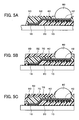
- interconnecting lines 40 are formed on the resin layer 20.
- the interconnecting lines 40 may be formed in one layer, or may be formed in multiple layers. For example, TiW and Cu layers may be deposited by sputtering, and then a Cu layer may be formed thereon by plating. For this formation process, well-known technology can be applied.
- the interconnecting lines 40 are formed to pass over the electrodes 16 (so as to be electrically connected to the electrodes 16).
- the interconnecting lines 40 may pass along the slanting surface 21.
- the interconnecting lines 40 are formed to extend to the region in which the recesses 22 are formed.
- the interconnecting lines 40 are formed to pass along the recesses 22.
- a part of the interconnecting lines 40 is formed on the inner surface of the recesses 22.
- the surface of the interconnecting lines 40 may be higher, even within the recesses 22, than the surface of the resin layer 20 (the surface in which the openings are formed).
- depressions may be formed over the recesses 22.
- the interconnecting lines 40 may be formed to have lands (areas wider than the line portions) 42.
- the lands 42 are for the purpose of providing external terminals 60 (see Fig. 5A) thereon.
- the lands 42 (only) may be formed over the recesses 22.
- a second resin layer 50 may be formed over the resin layer (first resin layer) 20, over the resin layer (first resin layer) 20, a second resin layer 50 may be formed.
- the description of the resin layer 20 may also be applied to the second resin layer 50.
- the second resin layer 50 may be a solder resist.
- the second resin layer 50 may be formed to cover the entirety of the interconnecting lines 40 or a part thereof (for example, a part excluding the central portion of the lands 42).
- the second resin layer 50 may be formed to cover a portion (for example, a scribing line or the vicinity of the electrodes 16) exposed from the resin layer 20 of the semiconductor substrate 10.
- the second resin layer 50 is formed so as, on the surface exposed from the interconnecting lines 40 of the resin layer 20, to enter the recesses 22.
- the second resin layer 50 may be patterned.
- the description of the patterning of the resin layer 20 can be applied.
- penetrating spaces are formed in the second resin layer 50.
- a part of the interconnecting lines 40 (for example, central portions of the lands 42) may be exposed from the second resin layer 50.
- the cutting region of the semiconductor substrate 10 may be exposed from the second resin layer 50.
- the second resin layer 50 may be left remaining to cover at least a part of the interconnecting lines 40.
- the second resin layer 50 may cover the electrical connection portion of the interconnecting lines 40 and electrodes 16.
- the second resin layer 50 may cover the interconnecting lines 40 over the slanting surface 21 of the resin layer 20.
- the second resin layer 50 may cover all except for the central portions of the lands 42 of the interconnecting lines 40.
- This embodiment includes the formation of recesses and projections on the second resin layer 50.
- a plurality of recesses 52 may be formed.
- the recesses 52 may be formed over the resin layer 20, and may be formed over a region of exposure from the resin layer 20 of the semiconductor substrate 10.
- the description of the recesses 22 may be applied.
- surface roughening may be applied, to form recesses and projections. For this surface roughening, the description of the surface roughening to which the resin layer 20 is subjected may be applied.
- external terminals 60 may be formed.
- the external terminals 60 may be formed of either of soft solder or hard solder.
- soft solder may be used solder not including lead (henceforth referred to as lead-free solder).
- lead-free solder may be used a tin-silver (Sn-Ag) type, tin-bismuth (Sn-Bi) type, tin-zinc (Sn-Zn) type, or tin-copper (Sn-Cu) type of alloy, or to any of these alloys may be further added at least one of silver, bismuth, zinc, and copper.
- conventional techniques can be applied for the formation of the external terminals 60.
- a third resin layer 70 may be formed on the second resin layer 50.
- the description of the resin layer 20 may also be applied to the third resin layer 70.
- the third resin layer 70 may be formed to cover the second resin layer 50.
- the third resin layer 70 may be formed to enter the recesses 52 in the second resin layer 50.
- the third resin layer 70 may be formed so that the cutting region of the semiconductor substrate 10 is exposed.
- the third resin layer 70 may cover the lateral surface of the edge of the cutting region of the second resin layer 50.
- the third resin layer 70 may cover a part of the external terminals 60 (for example, a root portion).
- the third resin layer 70 may be formed to cover the entirety of the semiconductor substrate 10, and subsequently patterned.
- the third resin layer 70 may be provided so that the external terminals 60 are covered, and subsequently the third resin layer 70 removed from the upper extremity of the external terminals 60.
- the description of the patterning of the resin layer 20 can be applied.
- a part of the third resin layer 70 may be removed.
- the use of a laser or ashing may also be applied to the patterning of the first or second resin layer 20 or 50.
- recesses and projections may be formed on the third resin layer 70.
- a plurality of recesses 72 may be formed in the third resin layer 70.
- the recesses 72 may be formed over the first and second resin layers 20 and 50.
- the description of the recesses 22 may be applied.
- surface roughening may be applied, to form recesses and projections. For this surface roughening, the description of the surface roughening to which the resin layer 20 is subjected may be applied.
- the third resin layer 70 may be formed so as to cover the external terminals 60, then in a step of removing (for example, ashing or the like) the third resin layer 70 from the upper extremity of the external terminals 60, surface roughening of other parts of the surface of the third resin layer 70 may be carried out.
- the semiconductor wafer of this embodiment comprises semiconductor substrate 10 made up of a plurality of integrated circuits 12, a resin layer 20 formed on the semiconductor substrate 10 and having a plurality of recesses formed in the surface, and interconnecting lines 40 formed to pass along the recesses 22 in the resin layer 20. More details are as described above.
- the semiconductor substrate 10 may be cut (for example, by scribing or dicing). If the first, second, and third resin layers 20, 50, and 70 are not provided in the cutting region of the semiconductor substrate 10, since the resin is not cut, clogging of the cutter (or blade) 80 can be prevented.
- Fig. 7 illustrates the semiconductor device of this embodiment.
- the semiconductor device comprises a semiconductor chip 90 having formed an integrated circuit 12, a resin layer 20 formed on the semiconductor chip 90 and having formed in the surface a plurality of recesses 22, and interconnecting lines 40 formed to pass along the recesses 22 over the resin layer 20.
- the semiconductor chip 90 may be cut from the semiconductor substrate 10. Other details are as described above.
- the adhesion properties of the resin layer 20 and the interconnecting lines 40 (for example, the lands 42 thereof), and the adhesion properties of the resin layer 20 and second resin layer 50 are good. If the surface of the resin layer 20 is subjected to surface roughening, then the adhesion properties are further improved. With regard to the adhesion properties, this applies also to the second and third resin layers 50 and 70. Also, since the recesses 22 are formed in the resin layer 20, light is reflected or refracted, and the opacity of the resin layer 20 is increased. For example, for light with a wavelength in the range 400 to 600 nm, the opacity is increased.
- the opacity is further increased. With regard to the opacity, this applies also to the second and third resin layers 50 and 70. By virtue of the high opacity of the resin layer 20 and so on, malfunction of the integrated circuit 12 is reduced.
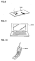
- Fig. 8 shows a circuit board 1000 on which is mounted the semiconductor device of the above described embodiment.
- Fig. 9 shows a notebook personal computer 2000
- Fig. 10 shows a mobile telephone 3000.
- the present invention includes substantially the same construction as the construction described in the embodiment (for example, a construction for which the function, method, and result are the same, or a construction of which the purpose and result are the same).
- the present invention includes a construction in which parts which are not of the essence of the construction described in the embodiment are replaced.
- the present invention includes a construction having the same effect as the construction described in the embodiment or a construction capable of achieving the same purpose.
- the present invention includes a construction having the construction described in the embodiment to which is added well-known art.
Landscapes
- Engineering & Computer Science (AREA)
- Structural Engineering (AREA)
- Architecture (AREA)
- Civil Engineering (AREA)
- Internal Circuitry In Semiconductor Integrated Circuit Devices (AREA)
- Encapsulation Of And Coatings For Semiconductor Or Solid State Devices (AREA)
- Dicing (AREA)
Applications Claiming Priority (2)
| Application Number | Priority Date | Filing Date | Title |
|---|---|---|---|
| JP2003036143 | 2003-02-14 | ||
| JP2003036143A JP3945415B2 (ja) | 2003-02-14 | 2003-02-14 | 半導体装置の製造方法 |
Publications (2)
| Publication Number | Publication Date |
|---|---|
| EP1458022A2 true EP1458022A2 (de) | 2004-09-15 |
| EP1458022A3 EP1458022A3 (de) | 2006-02-15 |
Family
ID=32767676
Family Applications (1)
| Application Number | Title | Priority Date | Filing Date |
|---|---|---|---|
| EP04001891A Withdrawn EP1458022A3 (de) | 2003-02-14 | 2004-01-29 | Halbleiteranordnung, Herstellungsverfahren dafür, Halbleiter-Substrat, Leiterplatte, und elektronischer Apparat |
Country Status (6)
| Country | Link |
|---|---|
| US (1) | US7135354B2 (de) |
| EP (1) | EP1458022A3 (de) |
| JP (1) | JP3945415B2 (de) |
| KR (1) | KR100646477B1 (de) |
| CN (1) | CN1258208C (de) |
| TW (1) | TWI239608B (de) |
Families Citing this family (16)
| Publication number | Priority date | Publication date | Assignee | Title |
|---|---|---|---|---|
| JP4124173B2 (ja) * | 2003-07-01 | 2008-07-23 | 日本電気株式会社 | 応力緩和構造とその形成方法、応力緩和シートとその製造方法、及び半導体装置並びに電子機器 |
| KR100611768B1 (ko) * | 2004-10-11 | 2006-08-10 | 삼성에스디아이 주식회사 | 유기전계발광표시장치 및 그 제조방법 |
| US8133808B2 (en) * | 2006-09-18 | 2012-03-13 | Tessera, Inc. | Wafer level chip package and a method of fabricating thereof |
| KR100787894B1 (ko) | 2007-01-24 | 2007-12-27 | 삼성전자주식회사 | 반도체 칩 구조물과 반도체 칩 구조물 제조 방법 그리고반도체 칩 패키지 및 반도체 칩 패키지 제조 방법 |
| US8564716B2 (en) * | 2007-11-21 | 2013-10-22 | Lg Innotek Co., Ltd. | Camera module |
| JP2009239106A (ja) * | 2008-03-27 | 2009-10-15 | Sony Corp | 半導体装置及び同半導体装置の製造方法 |
| KR101695772B1 (ko) * | 2009-08-19 | 2017-01-16 | 삼성전자주식회사 | 반도체 패키지 및 그 제조 방법 |
| US8426959B2 (en) * | 2009-08-19 | 2013-04-23 | Samsung Electronics Co., Ltd. | Semiconductor package and method of manufacturing the same |
| JP5968711B2 (ja) * | 2012-07-25 | 2016-08-10 | ルネサスエレクトロニクス株式会社 | 半導体装置及び半導体装置の製造方法 |
| US9355906B2 (en) | 2013-03-12 | 2016-05-31 | Taiwan Semiconductor Manufacturing Company, Ltd. | Packaging devices and methods of manufacture thereof |
| CN104051332B (zh) * | 2013-03-12 | 2017-04-12 | 台湾积体电路制造股份有限公司 | 封装器件及其制造方法 |
| US9728517B2 (en) * | 2013-12-17 | 2017-08-08 | Taiwan Semiconductor Manufacturing Company Ltd. | Semiconductor device and manufacturing method thereof |
| TW201812887A (zh) * | 2016-09-23 | 2018-04-01 | 頎邦科技股份有限公司 | 晶圓切割方法 |
| US10522526B2 (en) | 2017-07-28 | 2019-12-31 | Taiwan Semiconductor Manufacturing Company, Ltd. | LTHC as charging barrier in InFO package formation |
| US12406951B2 (en) | 2022-05-19 | 2025-09-02 | Nxp B.V. | Redistribution layer having a sideview zig-zag profile |
| US12119316B2 (en) | 2022-05-19 | 2024-10-15 | Nxp Usa, Inc. | Patterned and planarized under-bump metallization |
Family Cites Families (16)
| Publication number | Priority date | Publication date | Assignee | Title |
|---|---|---|---|---|
| JPH05267474A (ja) | 1992-03-18 | 1993-10-15 | Fujitsu Ltd | 半導体装置 |
| US5517758A (en) | 1992-05-29 | 1996-05-21 | Matsushita Electric Industrial Co., Ltd. | Plating method and method for producing a multi-layered printed wiring board using the same |
| CN1117512C (zh) | 1994-12-01 | 2003-08-06 | 揖斐电株式会社 | 多层印刷电路板及其制造方法 |
| KR100200687B1 (ko) | 1995-11-21 | 1999-06-15 | 윤종용 | 새로운 패드층을 구비하는 반도체장치 |
| US6316288B1 (en) | 1997-03-21 | 2001-11-13 | Seiko Epson Corporation | Semiconductor device and methods of manufacturing film camera tape |
| JP2000195896A (ja) * | 1998-12-25 | 2000-07-14 | Nec Corp | 半導体装置 |
| US6236114B1 (en) | 1999-05-06 | 2001-05-22 | Taiwan Semiconductor Manufacturing Co., Ltd. | Bonding pad structure |
| JP2000340696A (ja) | 1999-05-31 | 2000-12-08 | Matsushita Electric Works Ltd | 半導体パッケージの製造方法 |
| WO2000079589A1 (de) | 1999-06-17 | 2000-12-28 | Infineon Technologies Ag | Elektronisches bauelement mit flexiblen kontaktierungsstellen und verfahren zum herstellen eines derartigen bauelements |
| JP2001015560A (ja) | 1999-06-30 | 2001-01-19 | Toppan Printing Co Ltd | フィルムキャリアの製造方法 |
| JP2001085560A (ja) | 1999-09-13 | 2001-03-30 | Sharp Corp | 半導体装置およびその製造方法 |
| JP2001144217A (ja) | 1999-11-17 | 2001-05-25 | Seiko Epson Corp | 半導体装置及びその製造方法、回路基板並びに電子機器 |
| US6707153B2 (en) * | 2000-03-23 | 2004-03-16 | Seiko Epson Corporation | Semiconductor chip with plural resin layers on a surface thereof and method of manufacturing same |
| JP4750926B2 (ja) | 2000-06-06 | 2011-08-17 | 富士通セミコンダクター株式会社 | 半導体装置 |
| JP3440070B2 (ja) * | 2000-07-13 | 2003-08-25 | 沖電気工業株式会社 | ウェハー及びウェハーの製造方法 |
| US6713859B1 (en) * | 2000-09-13 | 2004-03-30 | Intel Corporation | Direct build-up layer on an encapsulated die package having a moisture barrier structure |
-
2003
- 2003-02-14 JP JP2003036143A patent/JP3945415B2/ja not_active Expired - Fee Related
-
2004
- 2004-01-21 US US10/763,858 patent/US7135354B2/en not_active Expired - Fee Related
- 2004-01-27 TW TW093101763A patent/TWI239608B/zh not_active IP Right Cessation
- 2004-01-29 EP EP04001891A patent/EP1458022A3/de not_active Withdrawn
- 2004-02-10 CN CNB200410003939XA patent/CN1258208C/zh not_active Expired - Fee Related
- 2004-02-13 KR KR1020040009446A patent/KR100646477B1/ko not_active Expired - Fee Related
Also Published As
| Publication number | Publication date |
|---|---|
| TW200423315A (en) | 2004-11-01 |
| TWI239608B (en) | 2005-09-11 |
| EP1458022A3 (de) | 2006-02-15 |
| JP2004247535A (ja) | 2004-09-02 |
| KR20040073984A (ko) | 2004-08-21 |
| US20040192024A1 (en) | 2004-09-30 |
| JP3945415B2 (ja) | 2007-07-18 |
| KR100646477B1 (ko) | 2006-11-14 |
| CN1521804A (zh) | 2004-08-18 |
| US7135354B2 (en) | 2006-11-14 |
| CN1258208C (zh) | 2006-05-31 |
Similar Documents
| Publication | Publication Date | Title |
|---|---|---|
| US7135354B2 (en) | Semiconductor device and method of manufacturing the same, semiconductor wafer, circuit board and electronic instrument | |
| KR100575591B1 (ko) | 웨이퍼 레벨 적층 패키지용 칩 스케일 패키지 및 그 제조 방법 | |
| US7264995B2 (en) | Method for manufacturing wafer level chip scale package using redistribution substrate | |
| US7132742B2 (en) | Semiconductor device, method of manufacturing the same, circuit board, and electronic instrument | |
| US20060076677A1 (en) | Resist sidewall spacer for C4 BLM undercut control | |
| US20040238926A1 (en) | Semiconductor wafer, semiconductor device and method for manufacturing same, circuit board, and electronic apparatus | |
| US7816790B2 (en) | Semiconductor device having low dielectric insulating film and manufacturing method of the same | |
| US20110127647A1 (en) | Semiconductor device and method for making the same | |
| US7183645B2 (en) | Semiconductor device with external terminal joined to concave portion of wiring layer | |
| US7323777B2 (en) | Semiconductor device, method of manufacturing the same, circuit board, and electronic instrument | |
| US7067929B2 (en) | Semiconductor wafer, semiconductor device, circuit board, electronic instrument, and method for manufacturing semiconductor device | |
| US6924558B2 (en) | Semiconductor device and method of fabricating the same, circuit board, and electronic instrument | |
| US6894394B2 (en) | Semiconductor device, circuit board, electronic apparatus, and method for manufacturing semiconductor device | |
| JP3623209B2 (ja) | 半導体装置及びその製造方法 | |
| JP3664167B2 (ja) | 半導体ウエハ、半導体装置及びその製造方法、回路基板並びに電子機器 | |
| JP4247611B2 (ja) | 半導体装置 | |
| JP2013026367A (ja) | 半導体装置及びその製造方法 | |
| US20240071762A1 (en) | Integrated circuit having an improved metal layer |
Legal Events
| Date | Code | Title | Description |
|---|---|---|---|
| PUAI | Public reference made under article 153(3) epc to a published international application that has entered the european phase |
Free format text: ORIGINAL CODE: 0009012 |
|
| AK | Designated contracting states |
Kind code of ref document: A2 Designated state(s): AT BE BG CH CY CZ DE DK EE ES FI FR GB GR HU IE IT LI LU MC NL PT RO SE SI SK TR |
|
| AX | Request for extension of the european patent |
Extension state: AL LT LV MK |
|
| PUAL | Search report despatched |
Free format text: ORIGINAL CODE: 0009013 |
|
| AK | Designated contracting states |
Kind code of ref document: A3 Designated state(s): AT BE BG CH CY CZ DE DK EE ES FI FR GB GR HU IE IT LI LU MC NL PT RO SE SI SK TR |
|
| AX | Request for extension of the european patent |
Extension state: AL LT LV MK |
|
| 17P | Request for examination filed |
Effective date: 20060727 |
|
| AKX | Designation fees paid |
Designated state(s): DE FR GB |
|
| 17Q | First examination report despatched |
Effective date: 20080414 |
|
| RTI1 | Title (correction) |
Free format text: METHOD OF MANUFACTURING A SEMICONDUCTOR DEVICE |
|
| GRAP | Despatch of communication of intention to grant a patent |
Free format text: ORIGINAL CODE: EPIDOSNIGR1 |
|
| STAA | Information on the status of an ep patent application or granted ep patent |
Free format text: STATUS: THE APPLICATION IS DEEMED TO BE WITHDRAWN |
|
| 18D | Application deemed to be withdrawn |
Effective date: 20091123 |