EP1457979A2 - Aufzeichnungssubstrat für Elektronenstrahl - Google Patents
Aufzeichnungssubstrat für Elektronenstrahl Download PDFInfo
- Publication number
- EP1457979A2 EP1457979A2 EP04003528A EP04003528A EP1457979A2 EP 1457979 A2 EP1457979 A2 EP 1457979A2 EP 04003528 A EP04003528 A EP 04003528A EP 04003528 A EP04003528 A EP 04003528A EP 1457979 A2 EP1457979 A2 EP 1457979A2
- Authority
- EP
- European Patent Office
- Prior art keywords
- electron beam
- resist film
- surface layer
- substrate
- layer area
- Prior art date
- Legal status (The legal status is an assumption and is not a legal conclusion. Google has not performed a legal analysis and makes no representation as to the accuracy of the status listed.)
- Withdrawn
Links
Images

Classifications
-
- G—PHYSICS
- G11—INFORMATION STORAGE
- G11B—INFORMATION STORAGE BASED ON RELATIVE MOVEMENT BETWEEN RECORD CARRIER AND TRANSDUCER
- G11B7/00—Recording or reproducing by optical means, e.g. recording using a thermal beam of optical radiation by modifying optical properties or the physical structure, reproducing using an optical beam at lower power by sensing optical properties; Record carriers therefor
- G11B7/24—Record carriers characterised by shape, structure or physical properties, or by the selection of the material
- G11B7/26—Apparatus or processes specially adapted for the manufacture of record carriers
- G11B7/261—Preparing a master, e.g. exposing photoresist, electroforming
-
- A—HUMAN NECESSITIES
- A47—FURNITURE; DOMESTIC ARTICLES OR APPLIANCES; COFFEE MILLS; SPICE MILLS; SUCTION CLEANERS IN GENERAL
- A47G—HOUSEHOLD OR TABLE EQUIPMENT
- A47G7/00—Flower holders or the like
- A47G7/02—Devices for supporting flower-pots or cut flowers
- A47G7/04—Flower tables; Stands or hangers, e.g. baskets, for flowers
- A47G7/044—Hanging flower-pot holders, e.g. mounted on walls, balcony fences or the like
-
- A—HUMAN NECESSITIES
- A01—AGRICULTURE; FORESTRY; ANIMAL HUSBANDRY; HUNTING; TRAPPING; FISHING
- A01G—HORTICULTURE; CULTIVATION OF VEGETABLES, FLOWERS, RICE, FRUIT, VINES, HOPS OR SEAWEED; FORESTRY; WATERING
- A01G5/00—Floral handling
- A01G5/04—Mountings for wreaths, or the like; Racks or holders for flowers
-
- G—PHYSICS
- G03—PHOTOGRAPHY; CINEMATOGRAPHY; ANALOGOUS TECHNIQUES USING WAVES OTHER THAN OPTICAL WAVES; ELECTROGRAPHY; HOLOGRAPHY
- G03F—PHOTOMECHANICAL PRODUCTION OF TEXTURED OR PATTERNED SURFACES, e.g. FOR PRINTING, FOR PROCESSING OF SEMICONDUCTOR DEVICES; MATERIALS THEREFOR; ORIGINALS THEREFOR; APPARATUS SPECIALLY ADAPTED THEREFOR
- G03F7/00—Photomechanical, e.g. photolithographic, production of textured or patterned surfaces, e.g. printing surfaces; Materials therefor, e.g. comprising photoresists; Apparatus specially adapted therefor
- G03F7/004—Photosensitive materials
- G03F7/09—Photosensitive materials characterised by structural details, e.g. supports, auxiliary layers
-
- H—ELECTRICITY
- H01—ELECTRIC ELEMENTS
- H01J—ELECTRIC DISCHARGE TUBES OR DISCHARGE LAMPS
- H01J2237/00—Discharge tubes exposing object to beam, e.g. for analysis treatment, etching, imaging
- H01J2237/30—Electron or ion beam tubes for processing objects
- H01J2237/317—Processing objects on a microscale
- H01J2237/3175—Lithography
- H01J2237/31793—Problems associated with lithography
Definitions
- the present invention relates to an electron beam recording substrate which holds a resist film where electron beam information recording is carried out.
- Information recording by an electron beam has been used in writing masks for semiconductor devices in order to improve the precision of line widths.
- an electron sensitive material is applied on a semiconductor substrate and an electron beam is directly irradiated on the electron sensitive material with the semiconductor substrate grounded.
- Optical discs or the like are formed by forming a stamper from a master disc acquired by exposing a resist film, made of an electron sensitive material coated on a disc substrate, with an electron beam to thereby form and record a latent image of track pattern information, and performing injection-molding with a synthetic resin using the stamper (see Japanese Unexamined Patent Publication No. 2002-230847, for example).
- the latent image on the resist film can be made finer by increasing the acceleration voltage in an electron gun.
- the increase in acceleration voltage leads a problem of lowering the sensitivity of the resist film for the following reason.
- the influence of forward scattering in the resist film becomes smaller, improving the contrast of the electron energy. This improves the resolution and the size controllability.
- electrons directly pass in the resist film, which lowers the sensitivity of the electron sensitive material.
- an electron beam recording substrate holds a resist film where electron beam information recording is carried out and has a surface layer area made of a material that suppresses enlargement of a scattering distribution diameter of electrons spread inside by irradiation of an electron beam from a resist film side.
- substrate an electron beam recording substrate
- This master disc is an information recording medium which becomes a master in fabricating high-density optical discs and is adapted to mastering technology using an electron beam.
- the outline of the electron beam mastering is such that a resist film is coated on an electron beam recording substrate, and then an electron beam exposure to directly irradiate an electron beam onto the resist film is performed, and then the exposed portion of the resist film is removed (formation of positive) by a developing process, thereby forming pits or grooves as recorded information on the resist film.
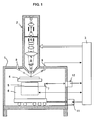
- Fig. 1 is a schematic block diagram illustrating the structure of an electron beam recorder or an information recording apparatus in electron beam mastering.
- the electron beam recorder comprises a vacuum chamber 1, an electron beam column 2 provided perpendicularly with respect to the vacuum chamber 1, and a controller 3.
- a spindle motor 5 which turns a master disc 4 while keeping it horizontal
- a movable stage 6 which moves the spindle motor 5 back and forth in a predetermined direction
- a mirror 7 attached to one end of the movable stage 6 and photosensors 8 and 9 for detecting the focal position of an electron beam.
- the master disc 4 placed on the turn table of the spindle motor 5 has a resist film deposited on that side of the electron beam column 2.
- the spindle motor 5 is controlled by the controller 3 in such a way as to rotate at a constant linear velocity at the time of electron beam exposure.
- the movable stage 6 is moved horizontally by the controller 3 upon reception of the driving force of an external electric motor 11.
- a distance measuring unit 12 which irradiates a laser beam on the mirror 7 and detects reflected light, detects the moving position of the movable stage 6 and supplies the position to the controller 3.
- the controller 3 performs feedback control of the movable stage 6.
- the electron beam column 2 comprises an electron gun, a condenser lens, a blanking electrode, an aperture, a deflection electrode, a focus lens, an objective lens, etc.
- the electron beam column 2 deflects electrons, radiated from the electron gun as an electron beam, via the condense lens and blanking electrode, performs beam modulation according to recorded information, adjusts the position by the deflection electrode, sets the focal distance by the focus lens, restricts the beam narrower by the objective lens, and irradiates the beam on the surface of the master disc 4. That is, the controller 3 performs the ON/OFF control and positional adjustment of the electron beam and focus control of the electron beam according to the irradiation position detection information from the photosensors 8 and 9.
- the spindle motor 5 and movable stage 6 are driven while irradiating the electron beam onto the surface of the thin film of the master disc 4, the master disc 4 is scanned with the electron beam. Accordingly, the resist film is exposed with the electron beam based on recorded information, and a latent image for minute recesses and projections, such as prepits and grooves, is formed on the resist film by the locus of the electron beam spot.
- Fig. 2 is a schematic cross-sectional views showing the structure of the master disc 4.
- the master disc 4 comprises an electron beam recording substrate (hereinafter called "substrate") S and a resist film R which is held on the substrate S and where information is recorded with an electron beam.
- the resist film R is coated by, for example, spin coating.
- the substrate S has a surface layer area 40 made of a material which suppresses enlargement of the scattering distribution ED diameter of electrons spread inside by irradiation of an electron beam from the resist film (R) side.
- the surface layer area 40 is in contact with the resist film R formed as a surface layer of a substrate main body MB in the substrate S.
- the entire substrate main body in contact with the resist film R can be made of a single material same as the material for the surface layer area 40, so that the surface layer area 40 itself can be made as a substrate.
- the present inventor studied the influence of the scattering distribution of electrons in the substrate on the amount of stored energy. The present inventor further discovered that the amount of stored energy, which would spread in the resist film due to scattering of input electrons, would be influenced by the scattering distribution of the electron beam, which passed the resist film, in the substrate.
- electrons enter the substrate they are elastically scattered with the nucleus of atoms constituting the substrate or perform non-elastic scattering with electrons constituting the substrate, thus increasing the width of the electron beam. Because part of the energy of the input electrons is given to the mating atoms or because of damping radiation discharge, the energy of electrons becomes smaller.
- the present inventor calculated the locus of electrons in the substrate through actual simulation and confirmed that the scattering distribution size over which the locus of electrons would be widened would vary significantly depending on the energy of the electron beam and the atomic number, density, etc. of a solid.
- n is the number of atoms per unit volume
- ⁇ is the scattering total cross-sectional area
- P is the atomic density
- A is the atomic weight.
- Z is the atomic number
- ⁇ is a screening parameter.
- the substrate including the surface layer area being made of a single material of magnesium (Mg), silicon (Si), titanium (Ti), nickel (Ni), ruthenium (Ru) and gold (Au), the locus of electrons in the surface layer area of the substrate and the electron beam energy which would reach the surface was simulated.
- the simulation was conducted under the conditions that the acceleration voltage V was 50 kV, the physical property values of the substrate's material were expressed by "element name (Z: atomic number, A: atomic weight, ⁇ : atomic density)" and were specifically given as Mg (Z: 12, A: 24.312, ⁇ : 1.738), Si (Z: 14, A: 28.086, ⁇ : 2.33), Ti (Z: 22, A: 47.90, ⁇ : 4.50), Ni (Z: 28, A: 58.71, ⁇ : 8.908), Ru (Z: 44, A: 101.07, ⁇ : 12.41) and Au (Z: 79, A: 196.97, ⁇ : 19.32).
- element name Z: atomic number, A: atomic weight, ⁇ : atomic density
- the entire substrate main body which is in contact with the resist film R as shown in Fig. 4 can be made of a single material and the substrate main body with the surface layer area 40 alone should be made of a material containing at least one of elements with atomic numbers 21 to 36, 38 to 54, 57 and 72 to 83 by 50 wt% or greater.
- the thickness of the surface layer area 40 may or may not exceed the diameter (depth) of the scattering distribution diameter ED.
- the surface layer area 40 should be made of a material containing at least one of elements with atomic numbers 73 to 79 by 50 wt% or greater and the substrate main body MB should be made of a material containing at least one of elements with atomic numbers 13, 14, 21 to 36, 38 to 54, 56, 57, 72 and 80 to 83 by 50 wt% or greater. This is because the use of such an element can enhance the scattering effect of the surface layer area 40.
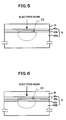
- the surface layer area 40 of the substrate can be constructed by plural layers of thin films, as shown in Fig. 5.
- at least one scattering layer 40a which is formed of an element with a high scattering effect should be made of a material containing at least one of elements with atomic numbers 21 to 36, 38 to 54, 56, 57, 72 to 83, more particularly, atomic numbers 73 to 79, by 50 wt% or greater.
- the element for a thin film 40b (auxiliary layer) other than the scattering layer 40a in the plurality of thin films of the surface layer area 40 should be selected from elements with a smaller average distance of ⁇ than the element for the scattering layer 40a.
- the scattering layer 40a is made of a material containing at least one of elements with atomic numbers 73 to 79 by 50 wt% or greater and the other thin films are made of a material containing at least one of elements with atomic numbers 21 to 36, 38 to 54, 56, 57, 72 and 80 to 83 by 50 wt% or greater.
- the scattering layer 40a in the surface layer area may be laid out in such a way as to contact the resist film.
- the scattering layer containing an element with a smaller average distance ⁇ than silicon it is possible to positively cause scattering of the electron beam that has entered the surface layer area of the substrate. At this time, it is difficult for the electrons to enter the surface layer area of the substrate so that a lot more scattered beam is concentrated on the surface layer area of the substrate, particularly, the scattering layer. This makes it possible to increase the number of electrons that contribute to the resist film formed on the surface layer area of the substrate. The increased electrons can enhance the sensitivity of the resist film.
- the most desirable element to be used for the scattering layer of the surface layer area of the substrate is a compound which essentially consists (50 wt% or more) of an element with the same atomic number as one of the atomic numbers 73 to 79 and the next candidate is a compound which essentially consists (50 wt% or more) of an element with the same atomic number as one of the atomic numbers 21 to 36, 38 to 54, 57, 72 and 80 to 83.
- the scattering layer of the surface layer area has a function of reducing the energy intensity of electrons scattered in the element with one of the atomic numbers 73 to 79 or its compound, resulting in a reduction in the electron energy which reaches the resist film and an improvement on the sensitivity.
- the multilayer surface layer area can be structured as another embodiment in such a way that as shown in Fig. 6, a further thin film 40c is provided between the scattering layer 40a and the resist film R and is made in contact with the resist film to avoid direct contact between the scattering layer and the resist film.
- the ⁇ ratio is reduced, i.e., ⁇ becomes smaller by forming the chromium layer to make the Au scattering layer into a non-contact type.
- the simulation showed that while electrons passing the chromium layer scattered, the scattering distribution of electrons passing the Au scattering layer became smaller and the electrons scattered in the silicon substrate main body, i.e., the scattering distribution of electrons became narrower at the Au scattering layer. Therefore, it was confirmed that placing the scattering layer containing an element with a small average distance 1, such as Au, in a middle of the lamination structure would allow the scattering layer to function as a filter and would reduce the energy dispersion of the surface layer area of the substrate.
- the electron beam which has scattered by the scattering layer alone scatters in the resist film in its high energy state seems less effective to achieve a high sensitivity (to improve the sensitivity of the resist film).
- the high sensitivity was achieved by making a multilayer structure comprising, for example, the scattering layer 40a and the auxiliary layer 40b and using the effect of reducing the energy of the scattered beam.
- an example of the master disc was prepared by forming a surface layer area having a chromium layer with a thickness of 100 nm and an Au scattering layer with a thickness of 300 nm laminated in this order on the silicon substrate main body and then forming a resist film with a predetermined thickness on the surface layer area.
- a line recording experiment at the recording speed of 0.7 to 1.4 m/s was conducted with an electron beam by irradiating an acceleration voltage of 50 kV onto the resist film of the master disc by an electron beam recorder.
- a comparative master disc having only a resist film formed on the silicon substrate was prepared. This master disc was also exposed with an electron beam and subject to a line recording experiment under the same conditions as those for the master disc example. The high-sensitivity achieving effects of both master discs were compared with each other by comparing the line widths of both master discs. The results are shown in Table 4 below. [m/s] Recording speed [nm] comparative master disc Master disc example 0.7 133 175 0.8 122 148 0.9 105 136 1.0 98 112 1.1 87 102 1.2 73 94 1.3 70 91 1.4 67 84
- the line width of the master disc example was increased as compared with that of the comparative master disc under the same recording condition. That is, Table 4 showed that the surface layer area of the substrate of the example had a high-sensitivity effect of increasing the energy density of the electron beam at the exposed portion of the resist film. As a result, it is possible to separate the exposed portion and non-exposed portion by a boundary surface with a sharp shape and achieve high density recording.
- the present invention can prepare a substrate having pre-patterns (servo patterns) formed concentrically and form a magnetic recording layer on that substrate to prepare a magnetic disc or a platter of a hard disc.
- the present invention which has been explained in case of sequential exposure with an electron beam by an electron beam recorder, the invention can also be applied to full exposure.
Landscapes
- Engineering & Computer Science (AREA)
- Manufacturing & Machinery (AREA)
- Life Sciences & Earth Sciences (AREA)
- Environmental Sciences (AREA)
- Exposure And Positioning Against Photoresist Photosensitive Materials (AREA)
- Materials For Photolithography (AREA)
- Manufacturing Optical Record Carriers (AREA)
- Preparing Plates And Mask In Photomechanical Process (AREA)
- Photoreceptors In Electrophotography (AREA)
- Electron Beam Exposure (AREA)
Applications Claiming Priority (2)
| Application Number | Priority Date | Filing Date | Title |
|---|---|---|---|
| JP2003052962 | 2003-02-28 | ||
| JP2003052962A JP2004264415A (ja) | 2003-02-28 | 2003-02-28 | 電子ビーム記録基板 |
Publications (2)
| Publication Number | Publication Date |
|---|---|
| EP1457979A2 true EP1457979A2 (de) | 2004-09-15 |
| EP1457979A3 EP1457979A3 (de) | 2007-05-09 |
Family
ID=32767827
Family Applications (1)
| Application Number | Title | Priority Date | Filing Date |
|---|---|---|---|
| EP04003528A Withdrawn EP1457979A3 (de) | 2003-02-28 | 2004-02-17 | Aufzeichnungssubstrat für Elektronenstrahl |
Country Status (6)
| Country | Link |
|---|---|
| US (1) | US20040170921A1 (de) |
| EP (1) | EP1457979A3 (de) |
| JP (1) | JP2004264415A (de) |
| KR (1) | KR100607426B1 (de) |
| CN (1) | CN1551169A (de) |
| TW (1) | TW200421337A (de) |
Families Citing this family (5)
| Publication number | Priority date | Publication date | Assignee | Title |
|---|---|---|---|---|
| KR20050072101A (ko) * | 2002-10-28 | 2005-07-08 | 마츠시타 덴끼 산교 가부시키가이샤 | 전자선 노광 방법 및 전자선 노광 장치 |
| TW200603150A (en) * | 2004-05-21 | 2006-01-16 | Pioneer Corp | Electron beam recording substrate |
| US20060018238A1 (en) * | 2004-07-21 | 2006-01-26 | Trepl John A Ii | Fabrication of digital media using electron beam technology |
| US20060018240A1 (en) * | 2004-07-21 | 2006-01-26 | Charles Marshall | Digital media created using electron beam technology |
| US20060072428A1 (en) * | 2004-09-03 | 2006-04-06 | Charles Marshall | Fabrication of digital media using ion beam technology |
Family Cites Families (18)
| Publication number | Priority date | Publication date | Assignee | Title |
|---|---|---|---|---|
| US3853715A (en) * | 1973-12-20 | 1974-12-10 | Ibm | Elimination of undercut in an anodically active metal during chemical etching |
| JPS5568626A (en) * | 1978-11-17 | 1980-05-23 | Chiyou Lsi Gijutsu Kenkyu Kumiai | Pattern formation |
| US5008734A (en) * | 1989-12-20 | 1991-04-16 | National Semiconductor Corporation | Stadium-stepped package for an integrated circuit with air dielectric |
| US5336892A (en) * | 1992-05-13 | 1994-08-09 | The United States Of America As Represented By The Secretary Of The Navy | Method and system for electron beam lithography |
| JPH06318038A (ja) * | 1993-05-07 | 1994-11-15 | Nitto Denko Corp | 個体識別ラベル |
| JPH06333806A (ja) * | 1993-05-19 | 1994-12-02 | Hitachi Ltd | 半導体集積回路装置の製造法 |
| KR100203893B1 (ko) * | 1995-06-16 | 1999-06-15 | 김영환 | 텅스텐 금속배선 형성방법 |
| US6015324A (en) * | 1996-12-30 | 2000-01-18 | Advanced Vision Technologies, Inc. | Fabrication process for surface electron display device with electron sink |
| JP3971500B2 (ja) * | 1998-02-20 | 2007-09-05 | ソニー株式会社 | 半導体素子実装用配線基板の製造方法 |
| JPH11344377A (ja) * | 1998-06-02 | 1999-12-14 | Matsushita Electric Ind Co Ltd | 赤外線検知素子およびその製造方法 |
| JPH11354423A (ja) * | 1998-06-05 | 1999-12-24 | Nikon Corp | 近接効果補正方法 |
| JP2001068412A (ja) * | 1998-06-12 | 2001-03-16 | Matsushita Electronics Industry Corp | パターン形成方法 |
| KR100548532B1 (ko) * | 1999-03-16 | 2006-02-02 | 주식회사 하이닉스반도체 | 스텐실 마스크 및 그 제조방법 |
| JP2000323377A (ja) * | 1999-05-07 | 2000-11-24 | Nikon Corp | 近接効果補正方法 |
| US6387787B1 (en) * | 2001-03-02 | 2002-05-14 | Motorola, Inc. | Lithographic template and method of formation and use |
| JP2003338091A (ja) * | 2002-05-22 | 2003-11-28 | Ricoh Co Ltd | 光ディスク用スタンパとその製造方法及び光ディスク |
| US6830871B2 (en) * | 2002-08-19 | 2004-12-14 | Fuji Photo Film Co., Ltd. | Chemical amplification type resist composition |
| US7049034B2 (en) * | 2003-09-09 | 2006-05-23 | Photronics, Inc. | Photomask having an internal substantially transparent etch stop layer |
-
2003
- 2003-02-28 JP JP2003052962A patent/JP2004264415A/ja active Pending
-
2004
- 2004-02-17 EP EP04003528A patent/EP1457979A3/de not_active Withdrawn
- 2004-02-18 TW TW093103963A patent/TW200421337A/zh unknown
- 2004-02-19 KR KR1020040010952A patent/KR100607426B1/ko not_active Expired - Fee Related
- 2004-02-27 US US10/787,407 patent/US20040170921A1/en not_active Abandoned
- 2004-02-27 CN CNA2004100072256A patent/CN1551169A/zh active Pending
Also Published As
| Publication number | Publication date |
|---|---|
| EP1457979A3 (de) | 2007-05-09 |
| US20040170921A1 (en) | 2004-09-02 |
| KR20040077471A (ko) | 2004-09-04 |
| TW200421337A (en) | 2004-10-16 |
| JP2004264415A (ja) | 2004-09-24 |
| CN1551169A (zh) | 2004-12-01 |
| KR100607426B1 (ko) | 2006-08-01 |
Similar Documents
| Publication | Publication Date | Title |
|---|---|---|
| EP1477847B1 (de) | Resistmaterial und mikrofabrikationsverfahren | |
| US20060076509A1 (en) | Electron beam irradiating method and manufacturing method of magnetic recording medium | |
| JP4058195B2 (ja) | ディスク原盤とディスク原盤形成装置並びにディスク原盤形成方法 | |
| EP1271502B1 (de) | Elektronenstrahlaufzeichnungsgerät und Verfahren | |
| EP1457979A2 (de) | Aufzeichnungssubstrat für Elektronenstrahl | |
| JP4090303B2 (ja) | 電子ビーム計測用センサー及び電子ビーム計測方法 | |
| DE19631928C2 (de) | Optische Speichervorrichtung zum Reproduzieren von Informationen von einem und/oder Aufzeichnen von Informationen auf einem optischen Speichermedium | |
| JPWO2011115139A1 (ja) | 電子ビーム露光方法および電子ビーム露光装置 | |
| US6773782B2 (en) | Magnetic memory medium having a magnetic film laminated on a substrate and a non-magnetic film formed thereon, and method of manufacturing the same | |
| US20040157346A1 (en) | Ion beam definition of magnetoresistive field sensors | |
| EP1560071A1 (de) | Elektronenstrahlbelichtungsverfahren und elektronenstrahlbelichtungssystem | |
| US6137660A (en) | Method for reducing ESD and imaging damage during focused ion beam definition of magnetoresistive head write track width | |
| EP1511026A2 (de) | Verfahren zur Herstellung einer Masterplatte für ein optisches Aufzeichnungsmedium, Verfahren zur Herstellung eines Musters, einer Mutterplatte, einer Matrize, eines optischen Aufzeichnungsmediums und eines Resists | |
| WO2005114332A1 (ja) | 電子ビーム記録基板 | |
| JP2002006509A (ja) | 露光方法及び光ディスク原盤の製造方法 | |
| JP3999579B2 (ja) | 電子線記録装置および電子線記録方法 | |
| JP3858609B2 (ja) | 情報記録方法及び情報記録媒体 | |
| JP2002299232A (ja) | ビーム照射方法及び装置 | |
| KR100299004B1 (ko) | 하전 입자빔으로 직접 기록하는 패턴 묘화 방법 | |
| US20080241308A1 (en) | Stamper for optical information recording medium, master for magnetic transfer, and manufacturing methods thereof | |
| JPH11288527A (ja) | 記録媒体製造用原盤の製造装置及び製造方法 | |
| JP2001267213A (ja) | レジストパターンの形成方法 | |
| JP2005049372A (ja) | 電子ビーム露光方法及びその装置 | |
| JP2004163698A (ja) | 電子線描画方法、電子線描画方法を用いて作成した原盤をもとに製作したスタンパ用金型、およびスタンパ用金型で製作した情報記録媒体 | |
| JP2006032813A (ja) | メンブレンマスクの製造方法 |
Legal Events
| Date | Code | Title | Description |
|---|---|---|---|
| PUAI | Public reference made under article 153(3) epc to a published international application that has entered the european phase |
Free format text: ORIGINAL CODE: 0009012 |
|
| AK | Designated contracting states |
Kind code of ref document: A2 Designated state(s): AT BE BG CH CY CZ DE DK EE ES FI FR GB GR HU IE IT LI LU MC NL PT RO SE SI SK TR |
|
| AX | Request for extension of the european patent |
Extension state: AL LT LV MK |
|
| PUAL | Search report despatched |
Free format text: ORIGINAL CODE: 0009013 |
|
| AK | Designated contracting states |
Kind code of ref document: A3 Designated state(s): AT BE BG CH CY CZ DE DK EE ES FI FR GB GR HU IE IT LI LU MC NL PT RO SE SI SK TR |
|
| AX | Request for extension of the european patent |
Extension state: AL LT LV MK |
|
| 17P | Request for examination filed |
Effective date: 20070704 |
|
| 17Q | First examination report despatched |
Effective date: 20070828 |
|
| AKX | Designation fees paid |
Designated state(s): DE FR GB |
|
| STAA | Information on the status of an ep patent application or granted ep patent |
Free format text: STATUS: THE APPLICATION IS DEEMED TO BE WITHDRAWN |
|
| 18D | Application deemed to be withdrawn |
Effective date: 20080108 |