EP1443652A2 - Schaltungsanordnung mit Phasendetektor und Phasenregelschleife mit der Schaltungsanordnung - Google Patents
Schaltungsanordnung mit Phasendetektor und Phasenregelschleife mit der Schaltungsanordnung Download PDFInfo
- Publication number
- EP1443652A2 EP1443652A2 EP04000558A EP04000558A EP1443652A2 EP 1443652 A2 EP1443652 A2 EP 1443652A2 EP 04000558 A EP04000558 A EP 04000558A EP 04000558 A EP04000558 A EP 04000558A EP 1443652 A2 EP1443652 A2 EP 1443652A2
- Authority
- EP
- European Patent Office
- Prior art keywords
- phase
- phase detector
- current source
- input
- output
- Prior art date
- Legal status (The legal status is an assumption and is not a legal conclusion. Google has not performed a legal analysis and makes no representation as to the accuracy of the status listed.)
- Granted
Links
Images

Classifications
-
- H—ELECTRICITY
- H03—ELECTRONIC CIRCUITRY
- H03L—AUTOMATIC CONTROL, STARTING, SYNCHRONISATION OR STABILISATION OF GENERATORS OF ELECTRONIC OSCILLATIONS OR PULSES
- H03L7/00—Automatic control of frequency or phase; Synchronisation
- H03L7/06—Automatic control of frequency or phase; Synchronisation using a reference signal applied to a frequency- or phase-locked loop
- H03L7/08—Details of the phase-locked loop
- H03L7/085—Details of the phase-locked loop concerning mainly the frequency- or phase-detection arrangement including the filtering or amplification of its output signal
- H03L7/089—Details of the phase-locked loop concerning mainly the frequency- or phase-detection arrangement including the filtering or amplification of its output signal the phase or frequency detector generating up-down pulses
- H03L7/0891—Details of the phase-locked loop concerning mainly the frequency- or phase-detection arrangement including the filtering or amplification of its output signal the phase or frequency detector generating up-down pulses the up-down pulses controlling source and sink current generators, e.g. a charge pump
- H03L7/0895—Details of the current generators
- H03L7/0898—Details of the current generators the source or sink current values being variable
-
- H—ELECTRICITY
- H03—ELECTRONIC CIRCUITRY
- H03L—AUTOMATIC CONTROL, STARTING, SYNCHRONISATION OR STABILISATION OF GENERATORS OF ELECTRONIC OSCILLATIONS OR PULSES
- H03L7/00—Automatic control of frequency or phase; Synchronisation
- H03L7/06—Automatic control of frequency or phase; Synchronisation using a reference signal applied to a frequency- or phase-locked loop
- H03L7/16—Indirect frequency synthesis, i.e. generating a desired one of a number of predetermined frequencies using a frequency- or phase-locked loop
- H03L7/18—Indirect frequency synthesis, i.e. generating a desired one of a number of predetermined frequencies using a frequency- or phase-locked loop using a frequency divider or counter in the loop
- H03L7/197—Indirect frequency synthesis, i.e. generating a desired one of a number of predetermined frequencies using a frequency- or phase-locked loop using a frequency divider or counter in the loop a time difference being used for locking the loop, the counter counting between numbers which are variable in time or the frequency divider dividing by a factor variable in time, e.g. for obtaining fractional frequency division
- H03L7/1974—Indirect frequency synthesis, i.e. generating a desired one of a number of predetermined frequencies using a frequency- or phase-locked loop using a frequency divider or counter in the loop a time difference being used for locking the loop, the counter counting between numbers which are variable in time or the frequency divider dividing by a factor variable in time, e.g. for obtaining fractional frequency division for fractional frequency division
- H03L7/1976—Indirect frequency synthesis, i.e. generating a desired one of a number of predetermined frequencies using a frequency- or phase-locked loop using a frequency divider or counter in the loop a time difference being used for locking the loop, the counter counting between numbers which are variable in time or the frequency divider dividing by a factor variable in time, e.g. for obtaining fractional frequency division for fractional frequency division using a phase accumulator for controlling the counter or frequency divider
Definitions
- the present invention relates to a circuit arrangement with phase detector and a phase locked loop with the Circuitry.
- Phase detectors are usually suitable for the phase position two at the inputs of the phase detector Compare signals with each other, a possibly existing one Determine phase deviation between the two input signals and to emit a signal at its output, which either is proportional or at least dependent on the phase difference of the input signals.
- Phase detectors are used, for example, in phase locked loops used to generate a signal with the desired frequency to snap onto a reference signal source.
- phase locked loops can produce high-precision signals with high frequency constancy generated by reference to a reference source, for example, a quartz oscillator becomes.
- the frequency generated can vary of the reference frequency. This is usually in the Feedback branch of the phase-locked loop a frequency divider intended.
- phase locked loop In order to use digital communication applications already at Frequency generation in the phase locked loop a carrier modulation can be achieved in further developments of the phase locked loop a so-called fractional-n frequency divider in the feedback path provided by the oscillator on the phase detector, with the fractional number ratio averaged over a time interval are adjustable.
- phase locked loops can, for example, from a digitally coded modulation signal can be controlled via so-called ⁇ converters.
- the output provided by a phase detector signal dependent on the phase difference of the input signals is usually put on a charge pump outlet, which produces an upward or downward stream, which in turn is usually integrated and in a corresponding Control voltage implemented a controllable oscillator in the Way controls that the phase difference at the input of the detector gets smaller until it disappears.
- phase detectors that not only have a phase difference, but also a frequency difference in the signal comparison of the input signals can be taken into account referred to as phase-frequency detectors.
- FIG. 3 A conventional phase detector arrangement is shown in FIG. 3. If one in the charge pump output stage 9 ', 13' Phase detector 1 the up and down current source 9 ', 13 'do not provide an ideally equal current for each Activation, there is a disadvantageous kink at the origin of the characteristic field of the charge pump phase detector unit, in Figure 4 as the characteristic curve the average Output current is plotted against the phase deviation the input signals of the detector. Because the origin, in which the characteristic curve kinks, but the operating point of the phase detector corresponds to an undesirable non-linearity at the working point. Especially with those described above Fractional-n phase locked loops, abbreviated to fractional-n-PLLs, but is a highly linear relationship between output current of the phase detector and phase difference of the input signals of particular importance for reliable function the circuit.
- the charge pump output stage of the phase detector equipped with a switchable reference power supply.
- the operating point of the phase detector circuit is thus advantageously from the origin of the characteristic curve, the output current plotted against the phase difference of the input signals represented, pushed out. Since the circuit according to working principle without a third power source can, is an implementation of the circuit with advantage small chip area and the operation of the circuit with small Power consumption possible.
- the proposed principle summarizes the advantageous Effect of the working point shift only through Switching the reference current from one of the two current sources reached.
- an offset current source can be used for Purpose of shifting the operating point advantageously dispensed with become.
- the positive works preferentially Power connection facing power source as a so-called Upward current source, which is a positive current from the signal output the circuit arrangement when activated drives, and the one facing the more negative supply connection Power source preferably works as a current sink, that means that a negative current flow from the signal output of the Switching out takes place.
- the second switch assigned to the second power source is preferably either in a series connection between the signal output of the circuit and one assigned to the current source Supply or reference potential connection provided.
- the second switch is for switching on and off the second power source is not connected to its load circuit, but designed to control the second power source assigned and driving this reference circuit.
- phase detector circuit Charge pump output stage is particularly advantageous Application in a PLL, phase locked loop, to advantage, because here a linear relationship between the output current of the Phase detector and phase difference of the input signals, in particular in the working point of the arrangement, particularly important is.
- the frequency divider is preferably designed as a fractional-n divider, and the phase locked loop is thus designed to operate as ⁇ modulator suitable according to digital modulation methods.
- FIG. 1 shows a circuit arrangement with phase detector according to the proposed principle.
- the phase detector 1 is designed as a phase-frequency detector and comprises an input 2 for supplying an input signal (IN1) with a first phase position ( ⁇ 1) and a further input 3 for supplying an input signal (IN2) with a second phase position ( ⁇ 2).
- Two outputs are provided at the output of the phase detector 1, an upward control signal at a first output 4 and a downward control signal at a second output 5 as a function of a phase difference ( ⁇ 2- ⁇ 1) between the input signals (IN1, IN2) Inputs (2, 3) of the detector 1 is provided.
- the output 4 of the phase detector is connected to the control input of a first switch 6, the output 5 of the phase detector is connected to the control input of a second switch 7.
- the switches 6, 7 control current source branches of a charge pump output stage 8 of the circuit arrangement with phase detector according to FIG. 1.
- a first current source 9, which works as an upward current source of the charge pump 8 is connected between a positive supply potential connection 10 and the signal output 11 of the circuit arrangement. Between the signal output 11 and a reference potential connection 12 of the circuit arrangement, a series circuit comprising the switch 7 and a second current source 13, which is designed as a downward current source of the charge pump 8 and works as a current sink, is connected.
- the first current source 9 has a reference current input 14, to which a reference current required to operate the current source is supplied.
- the output current of the first current source 9, which is provided with the reference symbol I UP is dependent on the reference current fed in at the input 14.
- the reference current input 14 is connected to a load connection of the switch 6 and is firmly connected to it.
- the switch 6 is designed as a changeover switch and is connected with a further load connection either to a first reference current source 15 or to a second reference current source 16.
- the reference current sources 15, 16 are designed to provide fixed but different reference currents I REF1 , I REF2 .
- the current source 9 Since according to the control and connection of the switch 6 with the quiescent current input or reference current input of the current source 9 and the two current sources 15, 16 to provide reference currents, the current source 9 is never completely switched off, but rather always delivers a certain amount of current to the signal output 11, that the characteristic of the phase detector, namely the output current I OUT plotted against the phase difference ⁇ 2- ⁇ 1 at the input of the detector 1 does not run through the origin, that is to say through the zero point. In turn, the working point of the phase detector arrangement of FIG. 1 is not in a possibly existing kink in the characteristic curve, which occurs when the current sources 9, 13 do not supply an ideally equal amount of current.
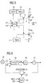
- FIG. 5 shows an alternative embodiment of the circuit arrangement with phase detector according to Figure 1. Same reference numerals denote the same or equivalent circuit parts.
- the circuit of Figure 5 corresponds in construction and advantageous function largely that of Figure 1 and differs only in that the switch 7 not in series with the second current source in the load circuit 13 is switched, but rather in the reference power supply the second current source 13 is connected.
- the desk 7 connects a third reference current source 17 on the load side a reference current input of the second current source 13.
- the Control input of the second switch 7 is at the second output 5 of the phase detector 1 placed.
- the second is on the load side Current source 13 now directly between the signal output 11 and the reference potential connection 12 switched.
- the circuit of FIG. 5 has an output stage 8 ' higher symmetry than that of the circuit of Figure 1.
- FIG. 6 shows a fractional N-PLL with a circuit arrangement 18 with phase detector 1 according to FIG. 1.
- the input 2 of the circuit arrangement with phase detector 18 of Figure 1 connected to a quartz oscillator 19.
- At exit 11 of the circuit arrangement 18 is via a stabilizing circuit Loop filter 20, the control input of a voltage-controlled oscillator 21 connected.
- the exit of the oscillator 21 forms the output of the entire one Phase locked loop and is also via a fractional-n frequency divider 22 to the further input 3 of the Circuit arrangement 18 with phase detector and charge pump output stage connected.
- the fractional-n frequency divider 22 is made up of a modulation signal MOD and a signal for Channel preselection CH controlled via a sigma-delta- ⁇ converter 23.
Landscapes
- Stabilization Of Oscillater, Synchronisation, Frequency Synthesizers (AREA)
Abstract
Description
- den Phasendetektor mit einem ersten Eingang zum Zuführen eines Eingangssignal mit einer ersten Phasenlage und mit einem zweiten Eingang zum Zuführen eines Eingangssignals mit einer zweiten Phasenlage,
- eine Ausgangsstufe mit einer ersten Stromquelle und mit einer zweiten Stromquelle,
- einen ersten Schalter zum Ansteuern der ersten Stromquelle, der einen Referenzstromeingang der Stromquelle entweder mit einer ersten Referenzstromquelle oder mit einer zweiten Referenzstromquelle koppelt und der einen Steuereingang aufweist, der an einen ersten Ausgang des Phasendetektors angeschlossen ist,
- einen zweiten Schalter, der zum Zu-/ und Abschalten der zweiten Stromquelle mit dieser gekoppelt ist, mit einem Steuereingang, der mit einem zweiten Ausgang des Phasendetektors verbunden ist, und
- einen Signalausgang der Schaltungsanordnung, der mit der ersten und der zweiten Stromquelle gekoppelt ist und der ausgelegt ist zur Bereitstellung eines Ausgangsstroms in Abhängigkeit von einer Phasenabweichung zwischen der ersten und der zweiten Phasenlage der Eingangssignale des Phasendetektors.
- einen gesteuerten Oszillator mit einem Steuereingang, der über ein Schleifenfilter an den Signalausgang der Schaltungsanordnung mit Phasendetektor angeschlossen ist, und mit einem Ausgang,
- einen Frequenzteiler, der den Ausgang des gesteuerten Oszillators mit dem ersten Eingang des Phasendetektors koppelt, und
- einen Bezugsfrequenz-Generator, der mit dem zweiten Eingang des Phasendetektors gekoppelt ist.
- Figur 1
- ein erstes Ausführungsbeispiel einer Schaltungsanordnung mit Phasendetektor gemäß dem vorgeschlagenen Prinzip,
- Figur 2
- die Kennlinie des Phasendetektors gemäß Figur 1,
- Figur 3
- einen herkömmlichen Phasendetektor mit Ladungspumpenausgang gemäß Stand der Technik,
- Figur 4
- die Kennlinie des Phasendetektors von Figur 3,
- Figur 5
- ein zweites Ausführungsbeispiel einer Phasendetektorschaltung gemäß dem vorgeschlagenen Prinzip anhand eines Schaltplans und
- Figur 6
- eine Phasenregelschleife mit Phasendetektorschaltung gemäß Figur 1 oder 5 anhand eines beispielhaften Blockschaltbilds.
- 1
- Phasendetektor
- 2
- Eingang
- 3
- Eingang
- 4
- Ausgang
- 5
- Ausgang
- 6
- Schalter
- 7
- Schalter
- 8
- Ausgangsstufe/Ladungspumpe
- 9
- Stromquelle
- 10
- Versorgungspotentialanschluß
- 11
- Signalausgang
- 12
- Bezugspotentialanschluß
- 13
- Stromquelle
- 14
- Referenzstromeingang
- 15
- Referenzstromquelle
- 16
- Referenzstromquelle
- 17
- Referenzstromquelle
- 18
- Phasendetektor mit Ladungspumpenausgang
- 19
- Quarz-Oszillator
- 20
- Schleifenfilter
- 21
- Spannungsgesteuerter Oszillator
- 22
- Fractional-n-Frequenzteiler
- 23
- ∑Δ-Wandler
Claims (6)
- Schaltungsanordnung mit Phasendetektor, aufweisendden Phasendetektor (1) mit einem ersten Eingang (3) zum Zuführen eines Eingangssignal mit einer ersten Phasenlage (Φ1) und mit einem zweiten Eingang (2) zum Zuführen eines Eingangssignals mit einer zweiten Phasenlage (Φ2),eine Ausgangsstufe (8) mit einer ersten Stromquelle (9) und mit einer zweiten Stromquelle (13),einen ersten Schalter (6) zum Ansteuern der ersten Stromquelle (9), der einen Referenzstromeingang der Stromquelle (9) entweder mit einer ersten Referenzstromquelle (15) oder mit einer zweiten Referenzstromquelle (16) koppelt und der einen Steuereingang aufweist, der an einen ersten Ausgang (4) des Phasendetektors (1) angeschlossen ist,einen zweiten Schalter (7), der zum Zu-/ und Abschalten der zweiten Stromquelle (13) mit dieser gekoppelt ist, mit einem Steuereingang, der mit einem zweiten Ausgang (5) des Phasendetektors (1) verbunden ist, undeinen Signalausgang (11) der Schaltungsanordnung, der mit der ersten und der zweiten Stromquelle (9, 13) gekoppelt ist und der ausgelegt ist zur Bereitstellung eines Ausgangsstroms in Abhängigkeit von einer Phasenabweichung zwischen der ersten und der zweiten Phasenlage (Φ1, Φ2) der Eingangssignale des Phasendetektors (1).
- Schaltungsanordnung nach Anspruch 1,
dadurch gekennzeichnet, daß
die erste und die zweite Stromquelle (9, 13) zur Bildung einer Serienschaltung zwischen einen Versorgungspotentialanschluß (10) und einen Bezugspotentialanschluß (12) in der Ausgangsstufe (8) der Schaltungsanordnung angeordnet sind. - Schaltungsanordnung nach Anspruch 1 oder 2
dadurch gekennzeichnet, daß
der zweite Schalter (7) die zweite Stromquelle (13) und den Signalausgang (11) der Schaltungsanordnung zu-/ und abschaltbar miteinander koppelt. - Schaltungsanordnung nach Anspruch 1 oder 2,
dadurch gekennzeichnet, daß
der zweite Schalter (7) einen Referenzstromeingang der zweiten Stromquelle mit einer dritten Referenzstromquelle (17) zu-/ und abschaltbar koppelt. - Phasenregelschleife mit einer Schaltungsanordnung gemäß einem der Patentansprüche 1 bis 4, aufweisendeinen gesteuerten Oszillator (21) mit einem Steuereingang, der über ein Schleifenfilter (20) an den Signalausgang der Schaltungsanordnung (18) mit Phasendetektor angeschlossen ist, und mit einem Ausgang,einen Frequenzteiler (22), der den Ausgang des gesteuerten Oszillators (21) mit dem ersten Eingang (3) des Phasendetektors (1) koppelt, undeinen Bezugsfrequenz-Generator (19), der mit dem zweiten Eingang (2) des Phasendetektors gekoppelt ist.
- Phasenregelschleife nach Anspruch 5,
dadurch gekennzeichnet, daß
der Frequenzteiler (22) als Fractional-N-Teiler ausgelegt ist, mit einem Steuereingang zum Zuführen eines aufbereiteten Modulationssignals.
Applications Claiming Priority (2)
| Application Number | Priority Date | Filing Date | Title |
|---|---|---|---|
| DE10303939 | 2003-01-31 | ||
| DE10303939A DE10303939B3 (de) | 2003-01-31 | 2003-01-31 | Schaltungsanordnung mit Phasendetektor und Phasenregelschleife mit der Schaltungsanordnung |
Publications (3)
| Publication Number | Publication Date |
|---|---|
| EP1443652A2 true EP1443652A2 (de) | 2004-08-04 |
| EP1443652A3 EP1443652A3 (de) | 2005-06-08 |
| EP1443652B1 EP1443652B1 (de) | 2008-10-01 |
Family
ID=32103478
Family Applications (1)
| Application Number | Title | Priority Date | Filing Date |
|---|---|---|---|
| EP04000558A Expired - Lifetime EP1443652B1 (de) | 2003-01-31 | 2004-01-13 | Schaltungsanordnung mit Phasendetektor und Phasenregelschleife mit der Schaltungsanordnung |
Country Status (4)
| Country | Link |
|---|---|
| US (1) | US6989699B2 (de) |
| EP (1) | EP1443652B1 (de) |
| CN (1) | CN1520030A (de) |
| DE (2) | DE10303939B3 (de) |
Families Citing this family (4)
| Publication number | Priority date | Publication date | Assignee | Title |
|---|---|---|---|---|
| CN1741389B (zh) * | 2004-08-26 | 2014-06-11 | 瑞昱半导体股份有限公司 | 具有非线性相位误差反应特性的锁相环 |
| US7535977B2 (en) * | 2004-09-30 | 2009-05-19 | Gct Semiconductor, Inc. | Sigma-delta based phase lock loop |
| TWI415394B (zh) * | 2010-04-13 | 2013-11-11 | Elite Semiconductor Esmt | 鎖相迴路電路及其操作方法 |
| EP3308428A1 (de) * | 2015-06-11 | 2018-04-18 | Telefonaktiebolaget LM Ericsson (publ) | Phasengesperrte schleifenanordnung, sender und empfänger und verfahren zur anpassung der phase zwischen oszillatorsignalen |
Family Cites Families (12)
| Publication number | Priority date | Publication date | Assignee | Title |
|---|---|---|---|---|
| DE58908860D1 (de) * | 1989-07-25 | 1995-02-16 | Siemens Ag | Schaltungsanordnung zur Nachlaufsynchronisation. |
| EP0595787B1 (de) * | 1990-05-21 | 1998-08-05 | Nec Corporation | Phasenregelkreisschaltung |
| US5208546A (en) * | 1991-08-21 | 1993-05-04 | At&T Bell Laboratories | Adaptive charge pump for phase-locked loops |
| JP2854777B2 (ja) * | 1992-04-27 | 1999-02-03 | 株式会社東芝 | 位相同期ループ回路と信号抽出方法 |
| US5699387A (en) * | 1993-06-23 | 1997-12-16 | Ati Technologies Inc. | Phase offset cancellation technique for reducing low frequency jitters |
| DE4342344C2 (de) * | 1993-12-11 | 1996-07-25 | Telefunken Microelectron | Schaltungsanordnung für eine Phasenregelschleife |
| KR100280452B1 (ko) * | 1998-03-17 | 2001-02-01 | 김영환 | 위상동기루프장치 |
| US6002273A (en) * | 1998-10-05 | 1999-12-14 | Motorola, Inc. | Linear low noise phase-frequency detector |
| JP3356277B2 (ja) * | 1999-09-14 | 2002-12-16 | 日本電気株式会社 | チャージポンプ回路及びpll回路 |
| KR100374631B1 (ko) * | 2000-06-09 | 2003-03-04 | 삼성전자주식회사 | 전하펌프 회로 |
| US6605935B2 (en) * | 2001-03-21 | 2003-08-12 | Telefonaktiebolaget L M Ericsson (Publ) | Linear fast-locking digital phase detector |
| US6756830B1 (en) * | 2003-01-14 | 2004-06-29 | Sharp Corporation | Charge pump for a current switch |
-
2003
- 2003-01-31 DE DE10303939A patent/DE10303939B3/de not_active Expired - Fee Related
-
2004
- 2004-01-13 EP EP04000558A patent/EP1443652B1/de not_active Expired - Lifetime
- 2004-01-13 DE DE502004008128T patent/DE502004008128D1/de not_active Expired - Lifetime
- 2004-01-29 US US10/769,464 patent/US6989699B2/en not_active Expired - Fee Related
- 2004-01-31 CN CNA200410004065XA patent/CN1520030A/zh active Pending
Also Published As
| Publication number | Publication date |
|---|---|
| DE10303939B3 (de) | 2004-05-13 |
| DE502004008128D1 (de) | 2008-11-13 |
| CN1520030A (zh) | 2004-08-11 |
| EP1443652B1 (de) | 2008-10-01 |
| EP1443652A3 (de) | 2005-06-08 |
| US6989699B2 (en) | 2006-01-24 |
| US20040183571A1 (en) | 2004-09-23 |
Similar Documents
| Publication | Publication Date | Title |
|---|---|---|
| DE10257185B3 (de) | Phasenregelschleife mit Sigma-Delta-Modulator | |
| DE102004020156A1 (de) | Einfangsbereich-Steuermechanismus für spannungsgesteuerte Oszillatoren | |
| DE2603641C2 (de) | Schaltungsanordnung zum Erzeugen eines stabilisierten Frequenzsignales | |
| DE2537329A1 (de) | Oszillatorschaltung | |
| DE102004060177B3 (de) | Polarmodulator und Verfahren zur Modulation eines Signals | |
| WO2004054107A2 (de) | Phasenregelkreis mit modulator | |
| WO2004042928A1 (de) | Schaltungsanordnung zur frequenzteilung und phasenregelschleife mit der schaltungsanordnung | |
| DE60209482T2 (de) | Gepufferte strom-gegengekoppelte stromversorgung und anwendungen hiervon | |
| DE3202733C2 (de) | ||
| DE69030276T2 (de) | Frequenzsynthetisierer | |
| DE10303939B3 (de) | Schaltungsanordnung mit Phasendetektor und Phasenregelschleife mit der Schaltungsanordnung | |
| DE19731478C2 (de) | Spannungsgesteuerter Doppeleingangsoszillator mit kompensierter Zweipunktfrequenz | |
| DE102005030356B4 (de) | Digitaler Phasenregelkreis und Verfahren zur Regelung eines digitalen Phasenregelkreises | |
| DE3003302C2 (de) | Stromgesteuerter Oszillator | |
| DE602006000532T2 (de) | Pulsgenerator | |
| DE9201910U1 (de) | Schaltungsanordnung zum Regeln der Frequenz der von einem Quarzoszillator abgegebenen Oszillatortaktsignale | |
| DE10139112B4 (de) | Spannungsgesteuerte Oszillatorschaltung | |
| DE3022287C2 (de) | Schaltung zur Kompensation von Frequenzschwankungen in FM-Systemen | |
| DE10255863B4 (de) | Phasenregelschleife | |
| DE3120930C2 (de) | ||
| EP1258063B1 (de) | Regelvorrichtung für laserdioden | |
| EP1030452B1 (de) | Phasenregelkreis | |
| DE3545771C2 (de) | ||
| WO2000014873A2 (de) | Schaltungsanordnung und verfahren zur takterzeugung | |
| DE10337285B4 (de) | Verstärkeranordnung |
Legal Events
| Date | Code | Title | Description |
|---|---|---|---|
| PUAI | Public reference made under article 153(3) epc to a published international application that has entered the european phase |
Free format text: ORIGINAL CODE: 0009012 |
|
| AK | Designated contracting states |
Kind code of ref document: A2 Designated state(s): AT BE BG CH CY CZ DE DK EE ES FI FR GB GR HU IE IT LI LU MC NL PT RO SE SI SK TR |
|
| AX | Request for extension of the european patent |
Extension state: AL LT LV MK |
|
| PUAL | Search report despatched |
Free format text: ORIGINAL CODE: 0009013 |
|
| AK | Designated contracting states |
Kind code of ref document: A3 Designated state(s): AT BE BG CH CY CZ DE DK EE ES FI FR GB GR HU IE IT LI LU MC NL PT RO SE SI SK TR |
|
| AX | Request for extension of the european patent |
Extension state: AL LT LV MK |
|
| RIC1 | Information provided on ipc code assigned before grant |
Ipc: 7H 03L 7/089 A Ipc: 7H 03L 7/197 B |
|
| 17P | Request for examination filed |
Effective date: 20051207 |
|
| AKX | Designation fees paid |
Designated state(s): DE FR GB IT |
|
| 17Q | First examination report despatched |
Effective date: 20060928 |
|
| GRAP | Despatch of communication of intention to grant a patent |
Free format text: ORIGINAL CODE: EPIDOSNIGR1 |
|
| GRAS | Grant fee paid |
Free format text: ORIGINAL CODE: EPIDOSNIGR3 |
|
| GRAA | (expected) grant |
Free format text: ORIGINAL CODE: 0009210 |
|
| AK | Designated contracting states |
Kind code of ref document: B1 Designated state(s): DE FR GB IT |
|
| REG | Reference to a national code |
Ref country code: GB Ref legal event code: FG4D Free format text: NOT ENGLISH |
|
| REF | Corresponds to: |
Ref document number: 502004008128 Country of ref document: DE Date of ref document: 20081113 Kind code of ref document: P |
|
| PLBE | No opposition filed within time limit |
Free format text: ORIGINAL CODE: 0009261 |
|
| STAA | Information on the status of an ep patent application or granted ep patent |
Free format text: STATUS: NO OPPOSITION FILED WITHIN TIME LIMIT |
|
| PG25 | Lapsed in a contracting state [announced via postgrant information from national office to epo] |
Ref country code: IT Free format text: LAPSE BECAUSE OF FAILURE TO SUBMIT A TRANSLATION OF THE DESCRIPTION OR TO PAY THE FEE WITHIN THE PRESCRIBED TIME-LIMIT Effective date: 20081001 |
|
| 26N | No opposition filed |
Effective date: 20090702 |
|
| REG | Reference to a national code |
Ref country code: GB Ref legal event code: 732E Free format text: REGISTERED BETWEEN 20110915 AND 20110921 |
|
| REG | Reference to a national code |
Ref country code: FR Ref legal event code: TP Owner name: INFINEON TECHNOLOGIES DELTA GMBH, DE Effective date: 20111102 |
|
| REG | Reference to a national code |
Ref country code: GB Ref legal event code: 732E Free format text: REGISTERED BETWEEN 20120223 AND 20120229 |
|
| REG | Reference to a national code |
Ref country code: FR Ref legal event code: TP Owner name: INTEL MOBILE COMMUNICATIONS GMBH, DE Effective date: 20120404 |
|
| REG | Reference to a national code |
Ref country code: DE Ref legal event code: R081 Ref document number: 502004008128 Country of ref document: DE Owner name: INTEL MOBILE COMMUNICATIONS GMBH, DE Free format text: FORMER OWNER: INFINEON TECHNOLOGIES DELTA GMBH, 85579 NEUBIBERG, DE Effective date: 20130306 Ref country code: DE Ref legal event code: R081 Ref document number: 502004008128 Country of ref document: DE Owner name: INTEL MOBILE COMMUNICATIONS GMBH, DE Free format text: FORMER OWNER: INTEL MOBILE COMMUNICATIONS TECHNOLOGY GMBH, 85579 NEUBIBERG, DE Effective date: 20130306 Ref country code: DE Ref legal event code: R081 Ref document number: 502004008128 Country of ref document: DE Owner name: INTEL MOBILE COMMUNICATIONS GMBH, DE Free format text: FORMER OWNER: INFINEON TECHNOLOGIES AG, 81669 MUENCHEN, DE Effective date: 20130306 Ref country code: DE Ref legal event code: R081 Ref document number: 502004008128 Country of ref document: DE Owner name: INTEL DEUTSCHLAND GMBH, DE Free format text: FORMER OWNER: INTEL MOBILE COMMUNICATIONS TECHNOLOGY GMBH, 85579 NEUBIBERG, DE Effective date: 20130306 Ref country code: DE Ref legal event code: R081 Ref document number: 502004008128 Country of ref document: DE Owner name: INTEL DEUTSCHLAND GMBH, DE Free format text: FORMER OWNER: INFINEON TECHNOLOGIES DELTA GMBH, 85579 NEUBIBERG, DE Effective date: 20130306 Ref country code: DE Ref legal event code: R081 Ref document number: 502004008128 Country of ref document: DE Owner name: INTEL DEUTSCHLAND GMBH, DE Free format text: FORMER OWNER: INFINEON TECHNOLOGIES AG, 81669 MUENCHEN, DE Effective date: 20130306 |
|
| REG | Reference to a national code |
Ref country code: GB Ref legal event code: 732E Free format text: REGISTERED BETWEEN 20131017 AND 20131023 |
|
| REG | Reference to a national code |
Ref country code: FR Ref legal event code: PLFP Year of fee payment: 12 |
|
| PGFP | Annual fee paid to national office [announced via postgrant information from national office to epo] |
Ref country code: GB Payment date: 20150107 Year of fee payment: 12 Ref country code: FR Payment date: 20150108 Year of fee payment: 12 |
|
| REG | Reference to a national code |
Ref country code: DE Ref legal event code: R081 Ref document number: 502004008128 Country of ref document: DE Owner name: INTEL DEUTSCHLAND GMBH, DE Free format text: FORMER OWNER: INTEL MOBILE COMMUNICATIONS GMBH, 85579 NEUBIBERG, DE |
|
| REG | Reference to a national code |
Ref country code: FR Ref legal event code: CD Owner name: INTEL DEUTSCHLAND GMBH, DE Effective date: 20160126 |
|
| PGFP | Annual fee paid to national office [announced via postgrant information from national office to epo] |
Ref country code: DE Payment date: 20160105 Year of fee payment: 13 |
|
| GBPC | Gb: european patent ceased through non-payment of renewal fee |
Effective date: 20160113 |
|
| REG | Reference to a national code |
Ref country code: FR Ref legal event code: ST Effective date: 20160930 |
|
| PG25 | Lapsed in a contracting state [announced via postgrant information from national office to epo] |
Ref country code: GB Free format text: LAPSE BECAUSE OF NON-PAYMENT OF DUE FEES Effective date: 20160113 |
|
| PG25 | Lapsed in a contracting state [announced via postgrant information from national office to epo] |
Ref country code: FR Free format text: LAPSE BECAUSE OF NON-PAYMENT OF DUE FEES Effective date: 20160201 |
|
| REG | Reference to a national code |
Ref country code: DE Ref legal event code: R119 Ref document number: 502004008128 Country of ref document: DE |
|
| PG25 | Lapsed in a contracting state [announced via postgrant information from national office to epo] |
Ref country code: DE Free format text: LAPSE BECAUSE OF NON-PAYMENT OF DUE FEES Effective date: 20170801 |