EP1440336B1 - Uv-bandpass filter and application to uv-detecting apparatus or light-emitting apparatus - Google Patents
Uv-bandpass filter and application to uv-detecting apparatus or light-emitting apparatus Download PDFInfo
- Publication number
- EP1440336B1 EP1440336B1 EP02743669A EP02743669A EP1440336B1 EP 1440336 B1 EP1440336 B1 EP 1440336B1 EP 02743669 A EP02743669 A EP 02743669A EP 02743669 A EP02743669 A EP 02743669A EP 1440336 B1 EP1440336 B1 EP 1440336B1
- Authority
- EP
- European Patent Office
- Prior art keywords
- light
- bandpass filter
- thin silver
- region
- silver film
- Prior art date
- Legal status (The legal status is an assumption and is not a legal conclusion. Google has not performed a legal analysis and makes no representation as to the accuracy of the status listed.)
- Expired - Lifetime
Links
- BQCADISMDOOEFD-UHFFFAOYSA-N Silver Chemical compound [Ag] BQCADISMDOOEFD-UHFFFAOYSA-N 0.000 claims description 81
- 229910052709 silver Inorganic materials 0.000 claims description 81
- 239000004332 silver Substances 0.000 claims description 81
- 238000002834 transmittance Methods 0.000 description 43
- 230000005540 biological transmission Effects 0.000 description 25
- 230000003287 optical effect Effects 0.000 description 11
- 239000000758 substrate Substances 0.000 description 8
- VYPSYNLAJGMNEJ-UHFFFAOYSA-N Silicium dioxide Chemical compound O=[Si]=O VYPSYNLAJGMNEJ-UHFFFAOYSA-N 0.000 description 6
- XUIMIQQOPSSXEZ-UHFFFAOYSA-N Silicon Chemical compound [Si] XUIMIQQOPSSXEZ-UHFFFAOYSA-N 0.000 description 6
- 230000035945 sensitivity Effects 0.000 description 6
- 229910052710 silicon Inorganic materials 0.000 description 6
- 239000010703 silicon Substances 0.000 description 6
- 239000000463 material Substances 0.000 description 5
- 230000001105 regulatory effect Effects 0.000 description 5
- 230000002787 reinforcement Effects 0.000 description 4
- 229910052724 xenon Inorganic materials 0.000 description 4
- FHNFHKCVQCLJFQ-UHFFFAOYSA-N xenon atom Chemical compound [Xe] FHNFHKCVQCLJFQ-UHFFFAOYSA-N 0.000 description 4
- 239000000853 adhesive Substances 0.000 description 3
- 230000001070 adhesive effect Effects 0.000 description 3
- 230000000903 blocking effect Effects 0.000 description 3
- 230000000052 comparative effect Effects 0.000 description 3
- 229910052736 halogen Inorganic materials 0.000 description 3
- 150000002367 halogens Chemical class 0.000 description 3
- VSQYNPJPULBZKU-UHFFFAOYSA-N mercury xenon Chemical compound [Xe].[Hg] VSQYNPJPULBZKU-UHFFFAOYSA-N 0.000 description 3
- 229910001507 metal halide Inorganic materials 0.000 description 3
- 150000005309 metal halides Chemical class 0.000 description 3
- 239000004065 semiconductor Substances 0.000 description 3
- 239000000919 ceramic Substances 0.000 description 2
- 230000007423 decrease Effects 0.000 description 2
- 239000011521 glass Substances 0.000 description 2
- 239000012535 impurity Substances 0.000 description 2
- 239000013307 optical fiber Substances 0.000 description 2
- 229920002050 silicone resin Polymers 0.000 description 2
- 239000004925 Acrylic resin Substances 0.000 description 1
- 229920000178 Acrylic resin Polymers 0.000 description 1
- ZOXJGFHDIHLPTG-UHFFFAOYSA-N Boron Chemical compound [B] ZOXJGFHDIHLPTG-UHFFFAOYSA-N 0.000 description 1
- OAICVXFJPJFONN-UHFFFAOYSA-N Phosphorus Chemical compound [P] OAICVXFJPJFONN-UHFFFAOYSA-N 0.000 description 1
- 229910052581 Si3N4 Inorganic materials 0.000 description 1
- 238000010521 absorption reaction Methods 0.000 description 1
- 229910052796 boron Inorganic materials 0.000 description 1
- 229910052681 coesite Inorganic materials 0.000 description 1
- 150000001875 compounds Chemical class 0.000 description 1
- 230000001276 controlling effect Effects 0.000 description 1
- 229910052906 cristobalite Inorganic materials 0.000 description 1
- 238000007599 discharging Methods 0.000 description 1
- 238000005516 engineering process Methods 0.000 description 1
- 238000000869 ion-assisted deposition Methods 0.000 description 1
- 238000005259 measurement Methods 0.000 description 1
- 229910052751 metal Inorganic materials 0.000 description 1
- 239000002184 metal Substances 0.000 description 1
- 238000012986 modification Methods 0.000 description 1
- 230000004048 modification Effects 0.000 description 1
- 230000000149 penetrating effect Effects 0.000 description 1
- 229910052698 phosphorus Inorganic materials 0.000 description 1
- 239000011574 phosphorus Substances 0.000 description 1
- 238000002310 reflectometry Methods 0.000 description 1
- 229920005989 resin Polymers 0.000 description 1
- 239000011347 resin Substances 0.000 description 1
- 239000000377 silicon dioxide Substances 0.000 description 1
- 239000002210 silicon-based material Substances 0.000 description 1
- 238000005476 soldering Methods 0.000 description 1
- 239000007787 solid Substances 0.000 description 1
- 230000003595 spectral effect Effects 0.000 description 1
- 229910052682 stishovite Inorganic materials 0.000 description 1
- 229910052905 tridymite Inorganic materials 0.000 description 1
- 238000007740 vapor deposition Methods 0.000 description 1
Images


Classifications
-
- G—PHYSICS
- G02—OPTICS
- G02B—OPTICAL ELEMENTS, SYSTEMS OR APPARATUS
- G02B5/00—Optical elements other than lenses
- G02B5/20—Filters
-
- G—PHYSICS
- G01—MEASURING; TESTING
- G01J—MEASUREMENT OF INTENSITY, VELOCITY, SPECTRAL CONTENT, POLARISATION, PHASE OR PULSE CHARACTERISTICS OF INFRARED, VISIBLE OR ULTRAVIOLET LIGHT; COLORIMETRY; RADIATION PYROMETRY
- G01J1/00—Photometry, e.g. photographic exposure meter
- G01J1/02—Details
- G01J1/08—Arrangements of light sources specially adapted for photometry standard sources, also using luminescent or radioactive material
-
- G—PHYSICS
- G02—OPTICS
- G02B—OPTICAL ELEMENTS, SYSTEMS OR APPARATUS
- G02B5/00—Optical elements other than lenses
- G02B5/20—Filters
- G02B5/208—Filters for use with infrared or ultraviolet radiation, e.g. for separating visible light from infrared and/or ultraviolet radiation
-
- G—PHYSICS
- G01—MEASURING; TESTING
- G01J—MEASUREMENT OF INTENSITY, VELOCITY, SPECTRAL CONTENT, POLARISATION, PHASE OR PULSE CHARACTERISTICS OF INFRARED, VISIBLE OR ULTRAVIOLET LIGHT; COLORIMETRY; RADIATION PYROMETRY
- G01J1/00—Photometry, e.g. photographic exposure meter
- G01J1/02—Details
- G01J1/04—Optical or mechanical part supplementary adjustable parts
- G01J1/0488—Optical or mechanical part supplementary adjustable parts with spectral filtering
-
- G—PHYSICS
- G01—MEASURING; TESTING
- G01J—MEASUREMENT OF INTENSITY, VELOCITY, SPECTRAL CONTENT, POLARISATION, PHASE OR PULSE CHARACTERISTICS OF INFRARED, VISIBLE OR ULTRAVIOLET LIGHT; COLORIMETRY; RADIATION PYROMETRY
- G01J1/00—Photometry, e.g. photographic exposure meter
- G01J1/42—Photometry, e.g. photographic exposure meter using electric radiation detectors
- G01J1/429—Photometry, e.g. photographic exposure meter using electric radiation detectors applied to measurement of ultraviolet light
Definitions
- the present invention relates to a UV-bandpass filter which selectively transmits therethrough light having a wavelength included in a UV-region, a UV-detecting apparatus including the same, and a UV source (light-emitting apparatus) including the same.
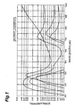
- an optical filter having a transmission characteristic with respect to light in a UV-region is, for example, one made by SCHOTT Corporation (catalog number: 3555eIX/84) having transmission characteristics such as those shown in Fig. 1 . While Fig. 1 shows transmission characteristics of four kinds of optical filters, each tends to exhibit transmission peaks in both UV- and IR-regions.
- silver films have been known to exhibit excellent spectral reflection characteristics with respect to light excluding the UV-region.
- an optical filter utilizing such a silver film is, for example, one using a silver film as a reflecting mirror disclosed in Japanese Patent Application Laid-Open No. SHO 60-252303 .
- This optical filter comprises such a structure that the silver film absorbs light in the UV-region but reflects light in the other wavelength regions, whereas light in the IR-region from the reflected light is blocked by use of a prism, so as to detect visible light.
- optical filters having transmission characteristics such as those shown in Fig. 1 surely exhibit an excellent transmission characteristic with respect to light in the UV-region, they also exhibit a transmission characteristic with respect to light in the IR-region near a wavelength of 700 nm.
- an optical filter having such transmission characteristics is utilized in an inexpensive light-receiving device mainly made of silicon, for example, having a light-receiving sensitivity up to near 1000 nm so as to be employed in a UV-detecting apparatus for detecting light included in the UV-region, UV-rays are hard to detect due to the transmission of light in the IR-region.
- the optical filter disclosed in Japanese Patent Application Laid-Open No. SHO 60-252303 utilizes a silver film as a reflecting mirror, it merely eliminates light in the UV-region by absorption, and is hard to apply to UV-detecting apparatus for detecting light in the UV-region.
- " Single films and heat mirrors produced by plasma ion assisted deposition" Journal of Non-Crystalline Solids, Vol. 218, pages 403-410 (1997 ) also discloses a reflecting mirror wherein the silver layer is a part of the a multilayer structure.
- An object of the present invention is to provide a UV-bandpass filter comprising a structure having anexcellent wavelength selectivity with a simple configuration while enabling wide applications, a UV-detecting apparatus including the same, and a UV source (light-emitting apparatus) including the same.
- the inventors have found that a single silver layer having an excellent transmission characteristic with respect to only light in a specific wavelength region included in the UV-region in a wide wavelength band ranging at least from 200 nm to 3000 nm can be obtained when transmission characteristics of a thin silver film is appropriately regulated by controlling its thickness.
- the optical filter selectively transmits light having a wavelength ranging from 250 nm to 400 nm, more preferably a wavelength ranging from 300 nm to 360 nm.
- the thin silver film has such a thickness as to exhibit a transmittance of 10% or less, preferably 5% or less, with respect to light having a wavelength excluding the specific UV-region.
- the inventors have found it necessary to suppress the transmittance for light having a wavelength of 400 nm or more to a value of 10% or less, preferably 5% or less, in order to make it possible to detect UV-rays, which necessitates a film thickness of 70 nm or more, preferably 80 nm or more.
- the inventors have found that a film thickness of 250 nm or less is required since it is necessary to secure a transmittance of 5% or more with respect to light in the above-mentioned specific UV-region in view of the light-receiving sensitivity of UV detectors.
- the UV-bandpass filter according to an embodiment of the present invention may be constituted by a member transparent to at least UV-rays (UV-transmitting member) prepared as a reinforcement member, and a thin silver film formed on a surface of the UV-transmitting member.
- UV-transmitting member UV-transmitting member
- the thin silver film may be directly or indirectly formed on a light entrance face of the light-receiving device.
- the light-receiving device has an entrance faceplate
- the thin silver film may be formed on the entrance faceplate as well (whereby the entrance faceplate functions as a reinforcement member for the thin silver film).
- the thin silver film maybe directly or indirectly formed on a light exit face of the UV source.
- the light-emitting device comprises an envelope which transmits light therethrough
- the thin silver film may be formed on a surface of the envelope (whereby the envelope itself functions as a reinforcement member for the thin silver film).
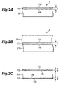
- Figs. 2A to 2C are views showing respective structures of first to third embodiments of the UV-bandpass filter according to the present invention.
- the UV-bandpass filter 1 according to the first embodiment shown in Fig. 2A comprises a UV-transmitting member 20, such as acrylic resin or silica glass, transparent to UV-rays and a thin silver film 10 having a thickness T (formable upon vapor deposition, for example) formed on a surface of the UV-transmitting member 20.
- the thin silver film 10 comprises an entrance face 10a and an exit face 10b for emitting light in a specific UV-region having a wavelength ranging from 200 nm to 400 nm, preferably a wavelength ranging from 250 nm to 400 nm, more preferably a wavelength ranging from 300 nm to 360 nm, in the light having reached the entrance face 10a.
- the thin silver film 10 has a thickness T of 70 nm or more, preferably 80 nm or less, so as to suppress the transmittance with respect to light having wavelengths excluding the specific UV-region to 10% or less, preferably 5% or less.
- it is necessary for the thickness T of the thin silver film 10 to be set to 250 nm or less in order to secure a transmittance of 5% ormore with respect to light having a wavelength included in the specific UV-region.
- the UV-bandpass filter 2 according to the second embodiment shown in Fig. 2B comprises a thin silver film 11 having a thickness T, while having a laminate structure in which a UV-transmitting member 21a and a UV-transmitting member 21b are in contact with the entrance face 11a and exit face 11b of the thin silver film 11, respectively.
- the UV-bandpass filter 2 according to the second embodiment is obtained when a surface of one of the UV-transmitting members 21a, 21b is formed with the thin silver film 11 and then the UV-transmitting members 21a, 21b are arranged so as to sandwitch thus formed thin silver film 11.
- the thin silver film 10 has a thickness T of 70 nm or more, preferably 80 nm or more, so as to suppress the transmittance with respect to light having wavelengths excluding the specific UV-region to 10% or less, preferably 5% or less, in the UV-bandpass filter 2 according to the second embodiment as well.
- the thickness T of the thin silver film 10 it is necessary for the thickness T of the thin silver film 10 to be set to 250 nm or less in order to secure a transmittance of 5% or more with respect to light having a wavelength included in the specific UV-region.
- the UV-bandpass filter 3 according to the third embodiment shown in Fig. 2C comprises a UV-transmitting member 22 and thin silver films 12, 13, each having a thickness T/2, formed on opposite main faces of the UV-transmitting member 22.
- the thin silver film 12 comprises an entrance face 12a and an exit face 12b for emitting light in the UV-region in the light having reached the entrance face 12a.
- the thin silver film 13 comprises an entrance face 13a and an exit face 13b for emitting light in the UV-region in the light having reached the entrance face 13a. It is not always necessary for the thin silver films 12, 13 to have the same thickness as long as their total thickness is T. Also, the number of thin silver films is not limited to 2 (the laminate structure may have two or more thin silver films having a total thickness of T).
- the total thickness (T) of the thin silver films 12, 13 is designed so as to become 70 nm or more, preferably 80 nm or more, in order to suppress the transmittance with respect to light having wavelengths excluding the specific UV-region to 10% or less, preferably 5% or less.
- the inventors prepared 11 kinds of samples having respective thicknesses (12.8 nm to 400.0 nm) different from each other, and measured transmission characteristics of these samples.
- Each of thus prepared samples comprised a structure similar to that of the UV-bandpass filter 1 according to the first embodiment shown in Fig. 2A , and was made by forming a thin silver film with a predetermined thickness on a surface of silica glass.
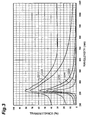
- Fig. 3 is a graph showing wavelength dependence characteristics concerning five kinds of thin silver films having thicknesses of 12.8 nm, 28.8 nm, 46.4 nm, 59.2 nm, and 78.4 nm, respectively;
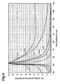
- Fig. 5 is a graph showing wavelength dependence characteristics concerning six kinds of thin silver films having thicknesses of 80.4 nm, 106.4 nm, 135.2 nm, 160.8 nm, 241.2 nm, and 400.0 nm, respectively.
- curves G210, G220, G230, G240, and G250 show wavelength dependence characteristics of transmittance concerning thin silver films having thicknesses of 12.8 nm, 28.8 nm, 46.4 nm, 59.2 nm, and 78.4 nm, respectively.
- Fig. 4 is a graph showing respective wavelength dependence characteristics of relative transmittance in the five kinds of thin silver films shown in Fig. 3 when their maximum transmittances are taken as 100%, in which curves G310, G320, G330, G340, and G350 correspond to curves G210, G220, G230, G240, and G250 in Fig. 3 , respectively.
- curves G410, G420, G430, G440, G450, and G460 show wavelength dependence characteristics of transmittance concerning thin silver films having thicknesses of 80.4 nm, 106.4 nm, 135.2 nm, 160.8 nm, 241.2 nm, and 400.0 nm, respectively.
- Fig. 6 is a graph showing respective wavelength dependence characteristics of relative transmittance in the six kinds of thin silver films shown in Fig. 5 when their maximum transmittances are taken as 100%, in which curves G510, G520, G530, G540, G550, and G560 correspond to curves G410, G420, G430, G440, G450, and G460 in Fig. 5 , respectively.
- each of the 11 kinds of prepared samples has a transmission characteristic in which only one peak exists at a wavelength of 322 nmin the wavelength band of 200 nm to 1000 nm. According to the measurement conducted by the inventors, only one transmission peak exists even in the wavelength band of 200 nm to 3000 nm.
- a thin silver film is employed in a UV-bandpass filter, it is necessary for the thin silver film to have a sufficient transmission characteristic with respect to light having a wavelength included in the UV-region (UV-rays) while having a sufficient blocking characteristic with respect to light having wavelengths excluding the UV-region.
- curve G610 shows the relationship between thickness and transmittance of a thin silver film with respect to light having a wavelength of 322 nm (transmission peak wavelength).
- a transmittance of at least 5% is required to be secured in order to make it possible for the light transmitted through the thin silver film (UV-rays) to be received by photodetectors. From this fact, it is seen that the maximum thickness of a thin silver film suitable for a UV-bandpass filter is preferably 250 nm or less.
- Fig. 8 is a graph showing respective relationships between thickness and relative transmittance with respect to a plurality of wavelengths (400 nm, 500 nm, and 600 nm) of light.
- the relative transmittance is a transmittance with reference to the maximum transmittance (taken as 100%) at a transmission peak wavelength of 322 nm.
- curves G710, G720, and G730 show relationships between thickness and relative transmittance with respect to light having wavelengths of 400 nm, 500 nm, and 600 nm, respectively.
- the minimum thickness of a thin silver film suitable for a UV-bandpass filter is required to be 70 nm or more, preferably 80 nm or more.
- Fig. 9 is a graph showing the ratio between transmittance of the UV-region (200 nm or more but 400 nm or less) and transmittance of wavelength (longer than 400 nm but 1000 nm or less) excluding the UV-region in the whole transmittance (measured in the wavelength range of 200 nm to 1000 nm) concerning a plurality of samples having film thicknesses (Ag film thicknesses) different from each other.
- region P1 indicates the ratio of transmittance in the UV-region
- region P2 shows the ratio of transmission of wavelengths excluding the UV-region.
- the ratio of wavelengths excluding the UV-region in the whole transmittance can be reduced to 10% or less if the film thickness is 70 nm or more, preferably 80 nm or more (the ratio of transmittance of wavelengths excluding the UV-region in the whole transmittance decreases to 1/10000 or less if the film thickness is about 240 nm).
- the UV-bandpass filter according to the present invention is constituted by a single silver layer regulated so as to have a predetermined thickness, whereby it can be combined with various kinds of optical devices such as light-receiving devices and light-emitting device.
- a UV-detecting apparatus employing the UV-bandpass filter according to the present invention will mainly be explained.
- Figs. 10A and 10B are views showing the exterior and sectional structure of first and second embodiments in the UV-detecting apparatus according to the present invention, respectively.
- the UV-detecting apparatus 300 comprises the simplest structure as shown in Fig. 10A , and is constituted by a UV-bandpass filter 1 such as the one shown in Fig. 2A , and a commercially available photodiode 30 (of can type).
- the UV-detecting apparatus 300 according to the first embodiment employs the UV-bandpass filter 1 having a thin silver film 10 formed on a UV-transmitting member 20 acting as a reinforcement plate, the thin silver film 10 may be formed on a surface 30a facing the photodiode 30 as well.
- Fig. 10B is a view showing the sectional structure of the UV-detecting apparatus 40 according to the second embodiment, in which the UV-bandpass filter 1 shown in Fig. 2A is employed as an entrance faceplate.
- the UV-detecting apparatus 40 according to the second embodiment comprises a ceramic case 41, lead pins 42 penetrating through the bottom part of the case 41, a photodiode 43 bonded to the bottom part of the case 41 with the aid of a die-bonding material 44, and an entrance faceplate (corresponding to the UV-bandpass filter 1) secured to the opening part of the case 41 by a silicone resin adhesive 45.
- the material of the case 41 is ceramic in the UV-detecting apparatus 40 according to the second embodiment, it may be a resin or metal as well.
- the photodiode 43 installed within the case 41 may be a semiconductor device such as phototransistor or avalanche photodiode, or a light-receiving IC or CCD accompanying circuits.
- the adhesive 45 for bonding the case 41 and the entrance faceplate, which is a UV-bandpass filter, to each other is not limited to silicone resins, but may be inorganic soldering materials or glass materials, for example, as long as they are adhesives which do not affect the transmission of UV-rays.
- the thin silver film constituting a part of the entrance faceplate may be formed on the surface opposing the photodiode 43 within the case 41 as well.
- Fig. 11 is a graph showing respective wavelength dependence characteristics of light-receiving sensitivity in the UV-detecting apparatus 40 having the structure shown in Fig. 10B and in a conventional photodetector (including no thin silver film as a UV-bandpass filter).
- thin silver films formed on the surface of silica glass 20 have thicknesses of 46.4 nm, 78.4 nm, and 106.4 nm, respectively.
- the photodiode prepared as the comparative example is a silicon photodiode.
- curves G810, G820, G830, and G840 show respective wavelength dependence characteristics of light-receiving sensitivity in the silicon photodiode and in the samples formed with thin silver films having thicknesses of 46.4 nm, 78.4 nm, and 106.4 nm, respectively.
- the photodetector (silicon photodiode), which is a comparative example, has a high light-receiving characteristic in the vicinity of 1000 nm (see curve G810), whereas each of the samples having a thin silver film formed on the entrance faceplate has only one transmission peak at a wavelength of 322 nm, thereby being able to effectively block light near a wavelength of 1000 nm (see curves G820, G830, and G840).
- those formed with thin respective silver films having thicknesses of 78.4 nm and 106.4 nm exhibit sufficient blocking characteristics with respect to light having wavelengths excluding the UV-region (see curves G830 and G840).
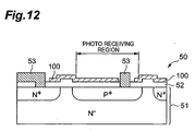
- Fig. 12 is a view showing the sectional structure of a third embodiment in the UV-detecting apparatus according to the present invention.
- the UV-detecting apparatus 50 (photodiode) according to the third embodiment comprises a monocrystal N-type silicon substrate 51.
- the substrate 51 is formed with a P + region in which impurities such as boron are injected, and an N + region in which impurities such as phosphorus are injected, whereas the front face of the substrate 51 is formed with an insulating film (SiO 2 or Si 3 N 4 ) 52 for protecting the surface of the substrate 51 and Al electrodes 53.
- a thin silver film 100 acting as the UV-bandpass filter according to the present invention, is directly formed on the light-receiving region of the photodiode comprising the foregoing configuration.
- the UV-bandpass filter is employed in a light-receiving device made of an inexpensive silicon material as such, a UV-detecting apparatus can be obtained at a lower cost.
- the insulating film 52 on the light-receiving region has a thickness regulated so as to yield a low reflectivity with respect to UV-rays, thereby improving the light-receiving sensitivity.
- an N + layer and an Au layer may successively be formed on the rear face of the substrate 51, so that the Au layer is employed as a signal-taking electrode.
- the substrate 51 is of N type, it may be of P type as well.
- the substrate material is not limited to silicon, but may be a compound semiconductor such as GaAsP, for example.
- the UV-detecting apparatus is a photodiode in which a thin silver film is formed as a UV-bandpass filter, it may also have a configuration in which a thin silver film is directly formed in the light-receiving region of a light-receiving IC or CCD accompanying circuits, or a semiconductor device such as phototransistor or avalanche photodiode.
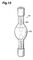
- Fig. 13 is a view showing the exterior of a first embodiment in the UV source (light-emitting apparatus) according to the present invention.
- the UV source 60 according to the first embodiment comprises a structure, for example, in which a thin silver film 610, which is a UV-bandpass filter according to the present invention, is directly formed on the surface of a glass envelope 600 of a xenon lamp emitting light upon discharging therewithin.
- the light-emitting apparatus according to the present invention is not limited to the xenon lamp as in the first embodiment, whereas UV sources can also be obtained in lamps of mercury-xenon, halogen, metal halide, and the like, for example.
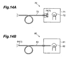
- Figs. 14A and 14B are views showing respective schematic structures of second and third embodiments in the UV source (light-emitting apparatus) according to the present invention.
- the UV source 70 comprises a lamp light source 72 of xenon, mercury-xenon, halogen, metal halide, and the like, a container 71 for accommodating the lamp light source 72, and a light valve 73 such as an optical fiber having a front end part secured to the container 71, whereas a UV-bandpass filter 74 is disposed between the light entrance end of the light valve 73 and the lamp light source 72.
- the UV source 70 according to the second embodiment shows the UV-bandpass filter 74 comprising a structure similar to that of the UV-bandpass filter 1 shown in Fig. 2A , it may be a UV-bandpass filter having a structure such as one shown in Fig. 2B or 2C as well. Also, it may have a structure in which a thin silver film is directly formed at the light entrance end of the light valve 73.
- the UV source 80 comprises a lamp light source 82 of xenon, mercury-xenon, halogen, metal halide, and the like, a container 81 for accommodating the lamp light source 82, and a light valve 83 such as an optical fiber having a front end part secured to the container 81, whereas a UV-bandpass filter 84 is disposed at the light exit end of the light valve 83.
- the UV source 80 according to the third embodiment also shows the UV-bandpass filter 84 comprising a structure similar to the UV-bandpass filter 1 shown in Fig. 2A , it may be a UV-bandpass filter having a structure such as one shown in Fig. 2B or 2C as well. Also, it may have a structure in which a thin silver film is directly formed at the light entrance end of the light valve 83.
- the thin silver film 10 which is a UV-bandpass filter, in each embodiment in the UV-bandpass filter, UV apparatus, and light-emitting apparatus according to the present invention, the thin silver film 10 also includes a film formed like an island having a gap of not greater than a wavelength of transmitted light.
- a single silver film regulated so as to have a predetermined thickness constitutes a bandpass filter having a sufficient blocking effect with respect to light having wavelengths excluding the UV-region, which is applicable to a wider range of technology when combined with conventional optical devices, and can function as a UV-bandpass filter in a wider wavelength band when the film thickness of the thin silver film is regulated to 70 nm or more, preferably 80 nm or more, but 250 nm or less.
Landscapes
- Physics & Mathematics (AREA)
- General Physics & Mathematics (AREA)
- Optics & Photonics (AREA)
- Health & Medical Sciences (AREA)
- Toxicology (AREA)
- Spectroscopy & Molecular Physics (AREA)
- Photometry And Measurement Of Optical Pulse Characteristics (AREA)
- Optical Filters (AREA)
Applications Claiming Priority (3)
| Application Number | Priority Date | Filing Date | Title |
|---|---|---|---|
| JP2001335392 | 2001-10-31 | ||
| JP2001335392A JP4213379B2 (ja) | 2001-10-31 | 2001-10-31 | 紫外線バンドパスフィルタ |
| PCT/JP2002/006182 WO2003038483A1 (en) | 2001-10-31 | 2002-06-20 | Uv-bandpass filter and application to uv-detecting apparatus or light-emitting apparatus |
Publications (2)
| Publication Number | Publication Date |
|---|---|
| EP1440336A1 EP1440336A1 (en) | 2004-07-28 |
| EP1440336B1 true EP1440336B1 (en) | 2008-10-01 |
Family
ID=19150386
Family Applications (1)
| Application Number | Title | Priority Date | Filing Date |
|---|---|---|---|
| EP02743669A Expired - Lifetime EP1440336B1 (en) | 2001-10-31 | 2002-06-20 | Uv-bandpass filter and application to uv-detecting apparatus or light-emitting apparatus |
Country Status (8)
| Country | Link |
|---|---|
| US (1) | US7405873B2 (enExample) |
| EP (1) | EP1440336B1 (enExample) |
| JP (1) | JP4213379B2 (enExample) |
| KR (1) | KR100870301B1 (enExample) |
| CN (1) | CN1238735C (enExample) |
| DE (1) | DE60229154D1 (enExample) |
| TW (1) | TW542907B (enExample) |
| WO (1) | WO2003038483A1 (enExample) |
Families Citing this family (19)
| Publication number | Priority date | Publication date | Assignee | Title |
|---|---|---|---|---|
| WO2004076997A1 (ja) * | 2003-02-28 | 2004-09-10 | Hamamatsu Photonics K.K. | 分光装置 |
| EP1673599A4 (en) * | 2003-09-29 | 2009-08-05 | Trojan Techn Inc | RADIATION SENSOR DEVICE AND RADIATION SOURCE MODULE THEREWITH |
| JP4370945B2 (ja) * | 2004-03-11 | 2009-11-25 | ソニー株式会社 | 誘電率の測定方法 |
| JP4344638B2 (ja) * | 2004-03-26 | 2009-10-14 | 富士フイルム株式会社 | 反射防止フィルム及びその製造方法、製造装置 |
| TWI271514B (en) * | 2005-02-21 | 2007-01-21 | Pixart Imaging Inc | UV sensor having a UV-pervious quartz glass |
| JP4324685B2 (ja) * | 2007-03-29 | 2009-09-02 | Okiセミコンダクタ株式会社 | 紫外線受光素子およびその製造方法、並びに紫外線量測定装置 |
| JP2010101627A (ja) * | 2008-10-21 | 2010-05-06 | Murata Mfg Co Ltd | 紫外線測定装置、コンパクトケースおよび電子機器 |
| US7967435B1 (en) * | 2010-04-21 | 2011-06-28 | 3M Innovative Properties Company | Metal detectable lens |
| WO2012081568A1 (ja) * | 2010-12-16 | 2012-06-21 | シャープ株式会社 | 蛍光体基板、表示装置および照明装置 |
| JP5834694B2 (ja) * | 2011-09-26 | 2015-12-24 | 株式会社ニデック | バンドパスフィルタ |
| CN103529506A (zh) * | 2013-09-27 | 2014-01-22 | 华侨大学 | 一种紫外荧光滤光片及其制备方法 |
| CN103513313A (zh) * | 2013-09-27 | 2014-01-15 | 华侨大学 | 一种皮肤损伤检测用的紫外荧光滤光片及其制备方法 |
| US12005266B2 (en) * | 2013-10-04 | 2024-06-11 | Strata Skin Sciences, Inc. | Device for targeted treatment of dermatosis |
| KR102219871B1 (ko) * | 2014-07-31 | 2021-02-25 | 스트라타 스킨 사이언시즈, 인코포레이티드 | 피부병의 표적 치료용 장치 |
| US20170028121A1 (en) * | 2015-07-31 | 2017-02-02 | Fenwal, Inc. | Irradiation device for biological fluids |
| WO2018123705A1 (ja) * | 2016-12-26 | 2018-07-05 | 旭硝子株式会社 | 紫外線透過フィルタ |
| CN111031212A (zh) * | 2019-12-20 | 2020-04-17 | Oppo广东移动通信有限公司 | 蓝玻璃滤光片及制备方法、摄像模组和电子设备 |
| EP4202507A4 (en) * | 2020-08-20 | 2024-09-11 | Nippon Electric Glass Co., Ltd. | OPTICAL FILTER, PROCESS FOR ITS PRODUCTION AND STERILIZATION DEVICE |
| KR102422624B1 (ko) | 2021-05-14 | 2022-07-20 | 영남대학교 산학협력단 | 자외선 필터 및 이를 포함하는 광학 램프 |
Family Cites Families (9)
| Publication number | Priority date | Publication date | Assignee | Title |
|---|---|---|---|---|
| JPS51131340A (en) | 1975-05-12 | 1976-11-15 | Hitachi Ltd | Optical interference filter |
| JPS60252303A (ja) | 1984-05-29 | 1985-12-13 | Anpuru Softwear Kk | 光学フイルタ |
| US4799745A (en) * | 1986-06-30 | 1989-01-24 | Southwall Technologies, Inc. | Heat reflecting composite films and glazing products containing the same |
| US5183700A (en) * | 1990-08-10 | 1993-02-02 | Viratec Thin Films, Inc. | Solar control properties in low emissivity coatings |
| TW205099B (enExample) * | 1991-05-30 | 1993-05-01 | Mitsui Toatsu Chemicals | |
| US5361172A (en) * | 1993-01-21 | 1994-11-01 | Midwest Research Institute | Durable metallized polymer mirror |
| JP2000180615A (ja) | 1998-12-11 | 2000-06-30 | Mitsui Chemicals Inc | 反射体及びそれを用いた反射部材 |
| JP2001154016A (ja) * | 1999-11-29 | 2001-06-08 | Marktec Corp | 紫外線透過フィルター及び該紫外線透過フィルターを用いた紫外線探傷灯 |
| US6587263B1 (en) * | 2000-03-31 | 2003-07-01 | Lockheed Martin Corporation | Optical solar reflectors |
-
2001
- 2001-10-31 JP JP2001335392A patent/JP4213379B2/ja not_active Expired - Fee Related
-
2002
- 2002-06-20 US US10/493,845 patent/US7405873B2/en not_active Expired - Fee Related
- 2002-06-20 CN CNB028214447A patent/CN1238735C/zh not_active Expired - Fee Related
- 2002-06-20 WO PCT/JP2002/006182 patent/WO2003038483A1/en not_active Ceased
- 2002-06-20 EP EP02743669A patent/EP1440336B1/en not_active Expired - Lifetime
- 2002-06-20 KR KR1020047006308A patent/KR100870301B1/ko not_active Expired - Fee Related
- 2002-06-20 DE DE60229154T patent/DE60229154D1/de not_active Expired - Fee Related
- 2002-06-25 TW TW091113915A patent/TW542907B/zh not_active IP Right Cessation
Also Published As
| Publication number | Publication date |
|---|---|
| JP2003139945A (ja) | 2003-05-14 |
| US20050063045A1 (en) | 2005-03-24 |
| KR20040111331A (ko) | 2004-12-31 |
| KR100870301B1 (ko) | 2008-11-25 |
| JP4213379B2 (ja) | 2009-01-21 |
| WO2003038483A1 (en) | 2003-05-08 |
| CN1578917A (zh) | 2005-02-09 |
| US7405873B2 (en) | 2008-07-29 |
| EP1440336A1 (en) | 2004-07-28 |
| TW542907B (en) | 2003-07-21 |
| CN1238735C (zh) | 2006-01-25 |
| DE60229154D1 (de) | 2008-11-13 |
Similar Documents
| Publication | Publication Date | Title |
|---|---|---|
| EP1440336B1 (en) | Uv-bandpass filter and application to uv-detecting apparatus or light-emitting apparatus | |
| CN113358223B (zh) | 光检测装置 | |
| EP3605043B1 (en) | Light detecting device | |
| TW202540615A (zh) | 濾光裝置 | |
| US7329876B2 (en) | Narrow-band transmission filter for EUV radiation | |
| WO2025157906A1 (en) | Camera modules incorporating metasurfaces | |
| JPWO2004076997A1 (ja) | 分光装置 | |
| JPH0743212A (ja) | 分光センサ | |
| JP2022145738A (ja) | フィルタ装置 | |
| EP2166383B1 (en) | Optical filter | |
| KR20110072503A (ko) | 빔 스플리터를 구비한 광 모듈 | |
| WO2006003843A1 (ja) | 光検出器 | |
| WO2025249030A1 (ja) | 光学素子及び光学装置 | |
| JP2025180930A (ja) | 光学素子及び光学装置 | |
| JP3803400B2 (ja) | 照度計の受光部 | |
| JP2025005376A (ja) | 角度選択的フィルタ | |
| JPH0448784A (ja) | 受光素子パッケージ | |
| KR20050017343A (ko) | 자외선에 대한 홍반 반응 센서와 부속 광학시스템 |
Legal Events
| Date | Code | Title | Description |
|---|---|---|---|
| PUAI | Public reference made under article 153(3) epc to a published international application that has entered the european phase |
Free format text: ORIGINAL CODE: 0009012 |
|
| 17P | Request for examination filed |
Effective date: 20040506 |
|
| AK | Designated contracting states |
Kind code of ref document: A1 Designated state(s): AT BE CH CY DE DK ES FI FR GB GR IE IT LI LU MC NL PT SE TR |
|
| AX | Request for extension of the european patent |
Extension state: AL LT LV MK RO SI |
|
| 17Q | First examination report despatched |
Effective date: 20040716 |
|
| GRAP | Despatch of communication of intention to grant a patent |
Free format text: ORIGINAL CODE: EPIDOSNIGR1 |
|
| GRAS | Grant fee paid |
Free format text: ORIGINAL CODE: EPIDOSNIGR3 |
|
| GRAA | (expected) grant |
Free format text: ORIGINAL CODE: 0009210 |
|
| AK | Designated contracting states |
Kind code of ref document: B1 Designated state(s): DE FR GB |
|
| REG | Reference to a national code |
Ref country code: GB Ref legal event code: FG4D |
|
| REF | Corresponds to: |
Ref document number: 60229154 Country of ref document: DE Date of ref document: 20081113 Kind code of ref document: P |
|
| PLBE | No opposition filed within time limit |
Free format text: ORIGINAL CODE: 0009261 |
|
| STAA | Information on the status of an ep patent application or granted ep patent |
Free format text: STATUS: NO OPPOSITION FILED WITHIN TIME LIMIT |
|
| 26N | No opposition filed |
Effective date: 20090702 |
|
| GBPC | Gb: european patent ceased through non-payment of renewal fee |
Effective date: 20090620 |
|
| REG | Reference to a national code |
Ref country code: FR Ref legal event code: ST Effective date: 20100226 |
|
| PG25 | Lapsed in a contracting state [announced via postgrant information from national office to epo] |
Ref country code: FR Free format text: LAPSE BECAUSE OF NON-PAYMENT OF DUE FEES Effective date: 20090630 |
|
| PG25 | Lapsed in a contracting state [announced via postgrant information from national office to epo] |
Ref country code: GB Free format text: LAPSE BECAUSE OF NON-PAYMENT OF DUE FEES Effective date: 20090620 |
|
| PG25 | Lapsed in a contracting state [announced via postgrant information from national office to epo] |
Ref country code: DE Free format text: LAPSE BECAUSE OF NON-PAYMENT OF DUE FEES Effective date: 20100101 |