EP1436765B1 - Adapter zum kontaktieren von chipkarten - Google Patents
Adapter zum kontaktieren von chipkarten Download PDFInfo
- Publication number
- EP1436765B1 EP1436765B1 EP02801891A EP02801891A EP1436765B1 EP 1436765 B1 EP1436765 B1 EP 1436765B1 EP 02801891 A EP02801891 A EP 02801891A EP 02801891 A EP02801891 A EP 02801891A EP 1436765 B1 EP1436765 B1 EP 1436765B1
- Authority
- EP
- European Patent Office
- Prior art keywords
- circuit board
- adapter
- elements
- receiving channel
- spring elements
- Prior art date
- Legal status (The legal status is an assumption and is not a legal conclusion. Google has not performed a legal analysis and makes no representation as to the accuracy of the status listed.)
- Expired - Lifetime
Links
Images


Classifications
-
- G—PHYSICS
- G06—COMPUTING; CALCULATING OR COUNTING
- G06K—GRAPHICAL DATA READING; PRESENTATION OF DATA; RECORD CARRIERS; HANDLING RECORD CARRIERS
- G06K19/00—Record carriers for use with machines and with at least a part designed to carry digital markings
- G06K19/06—Record carriers for use with machines and with at least a part designed to carry digital markings characterised by the kind of the digital marking, e.g. shape, nature, code
- G06K19/067—Record carriers with conductive marks, printed circuits or semiconductor circuit elements, e.g. credit or identity cards also with resonating or responding marks without active components
- G06K19/07—Record carriers with conductive marks, printed circuits or semiconductor circuit elements, e.g. credit or identity cards also with resonating or responding marks without active components with integrated circuit chips
- G06K19/077—Constructional details, e.g. mounting of circuits in the carrier
- G06K19/07737—Constructional details, e.g. mounting of circuits in the carrier the record carrier consisting of two or more mechanically separable parts
- G06K19/07741—Constructional details, e.g. mounting of circuits in the carrier the record carrier consisting of two or more mechanically separable parts comprising a first part operating as a regular record carrier and a second attachable part that changes the functional appearance of said record carrier, e.g. a contact-based smart card with an adapter part which, when attached to the contact card makes the contact card function as a non-contact card
-
- G—PHYSICS
- G06—COMPUTING; CALCULATING OR COUNTING
- G06K—GRAPHICAL DATA READING; PRESENTATION OF DATA; RECORD CARRIERS; HANDLING RECORD CARRIERS
- G06K7/00—Methods or arrangements for sensing record carriers, e.g. for reading patterns
- G06K7/0013—Methods or arrangements for sensing record carriers, e.g. for reading patterns by galvanic contacts, e.g. card connectors for ISO-7816 compliant smart cards or memory cards, e.g. SD card readers
- G06K7/0047—Methods or arrangements for sensing record carriers, e.g. for reading patterns by galvanic contacts, e.g. card connectors for ISO-7816 compliant smart cards or memory cards, e.g. SD card readers for reading/sensing record carriers having edge contacts
-
- H—ELECTRICITY
- H01—ELECTRIC ELEMENTS
- H01R—ELECTRICALLY-CONDUCTIVE CONNECTIONS; STRUCTURAL ASSOCIATIONS OF A PLURALITY OF MUTUALLY-INSULATED ELECTRICAL CONNECTING ELEMENTS; COUPLING DEVICES; CURRENT COLLECTORS
- H01R13/00—Details of coupling devices of the kinds covered by groups H01R12/70 or H01R24/00 - H01R33/00
- H01R13/02—Contact members
- H01R13/22—Contacts for co-operating by abutting
- H01R13/24—Contacts for co-operating by abutting resilient; resiliently-mounted
-
- H—ELECTRICITY
- H01—ELECTRIC ELEMENTS
- H01R—ELECTRICALLY-CONDUCTIVE CONNECTIONS; STRUCTURAL ASSOCIATIONS OF A PLURALITY OF MUTUALLY-INSULATED ELECTRICAL CONNECTING ELEMENTS; COUPLING DEVICES; CURRENT COLLECTORS
- H01R2201/00—Connectors or connections adapted for particular applications
- H01R2201/06—Connectors or connections adapted for particular applications for computer periphery
Definitions
- the invention relates to an adapter for contacting smart cards, in particular with a standardized according to the PCMCIA standard connection of a data processing device, with a card-shaped housing, which opens at one end into a receiving channel insertion slot for receiving a smart card and arranged on the opposite end Having terminal array, and with an electrically connected to the pad circuit board, which extends parallel to the receiving channel and is provided with contact elements for contacting the chip card.
- a chip card designed as a contact reader units which allow in the form of an adapter system, for example, a Chip card to connect to a standard PCMCIA standard connection of a data processing system.
- the known in the art for this purpose adapters have a PCMCIA plug-in socket, which causes a mechanical and electrical contact with a PCMCIA slot of the data processing system.
- the read-out of the chip card takes place via arranged in the receiving channel for the chip card contact elements which contact the same touching or, for example, on optical or magnetic way, without contact.
- An adapter for contacting chip cards is known, for example, from US Pat. No. 6,272,017 B1.
- the adapter has a card-shaped housing with an opening on a front side opening into a receiving channel slot for receiving a smart card and a arranged on the opposite end side panel.
- a printed circuit board is electrically connected, which extends parallel to the receiving channel and is provided with contact elements for contacting the chip card.
- a contacting unit for card-shaped carrier elements of electronic assemblies comprising a base plate with a plane-parallel recording of a card-shaped support member suitable size, at least one arranged substantially parallel to the base plate circuit board with contact elements for the electronic components of the support element its surface and is provided with a arranged at one edge of the base plate connection panel.
- a to the base plate substantially congruent, plate-shaped cover member forms with the circuit board a slot-like insertion channel and is attached to the base plate in the region of the connection pad and the opposite corners. Due to the mounting in the housing, the printed circuit board fills the full installation space in the housing.
- the invention has for its object to provide an adapter for contacting smart cards, in particular with a standard PCMCIA standard connection of a data processing device or the like, the above mentioned type, to the effect that the economic benefits of higher component integration can be used by the PCB manufacturing, so that a simple and cost-effective production can be achieved, which ensures an economical mass production, especially in view of the increasingly extensive use of prescribed card systems.
- the circuit board in the extension direction of the receiving channel has a relation to the receiving channel shortened length and the insertion slot facing end side with a device for positioning the circuit board and for guiding the chip card in the receiving channel is provided.
- the invention which is defined in the claims, is based on the recognition that the printed circuit board surface must be reduced in order to take advantage of the economic advantages of higher component integration. This reduction not only brings savings in PCB base material, but also benefits in PCB manufacturing.
- the device according to the invention for positioning the printed circuit board and for guiding the chip card in the receiving channel simultaneously ensures reliable contacting of a chip card inserted into the receiving channel, so that the two cost advantages, the saving of printed circuit board base material on the one hand and the increase in benefits in printed circuit board production on the other hand, are usable.
- Such a ausgestalteter adapter can be easily and inexpensively manufactured and therefore allows a mass production in the aforementioned sense. This is due to the fact that the advantageously the circuit board floating einklemmende means for a secure positioning of the shortened circuit board in the receiving channel of the housing of the adapter and on the other a secure guidance and contacting the chip card in the receiving channel of the housing of the adapter between the circuit board and the upper cover plate ensured the housing of the adapter.
- the plug-card-shaped housing on one end face has a slot for receiving a memory card and on the opposite end face a pad which is electrically connected to a printed circuit board arranged in the housing.
- the circuit board is in the known adapter shorter than the overall length of the housing, but the memory card is not - as in the invention - pushed over or under the circuit board, so that the contact fields of the memory card and the circuit board face each other, but the receiving channel of the housing is arranged such that the memory card to be read out is brought to the end of the circuit board and contacted via contact pins also on the front side.
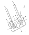
- the device for positioning the printed circuit board arm-shaped support members and arm-shaped spring elements with a fixed end and a free end, wherein the free ends of the support members and the spring elements on opposite sides of the circuit board extending in the direction of the pad.
- the arm-shaped support elements and spring elements thus provide functional elements for the chip card guide and the printed circuit board receptacle.
- the circuit board is clamped floating between the arm-shaped support members and the arm-shaped spring elements. Characterized in that the device is connected directly to the circuit board, the PCB length is variable depending on the application without changes to the housing of the adapter or the receiving channel.
- PCMCIA adapter instead of usual for PCMCIA adapter
- the arm-shaped spring elements cam-shaped locking means, which engage in corresponding thereto provided on the sides of the circuit board receptacles.
- the cam-shaped latching means are advantageously arranged at the free end of the spring element and the receptacles are holes formed in the printed circuit board, preferably catching holes, or recesses formed in the printed circuit board.
- the locking means ensure a secure connection between the circuit board and the device.
- the spring elements guide and / or abutment means for positioning the circuit board on the device are formed as arranged on the spring elements tabs which are aligned with the longitudinal sides of the circuit board.
- the device has two support elements and two spring elements, which extend in the extension direction of the receiving channel parallel to and at a distance from each other and perpendicular to the extension direction of the receiving channel from each other.
- the support elements and the spring elements are arranged symmetrically to the front side, preferably such that the spring elements are outside and the support elements inside, particularly preferably such that the support elements are positioned to the left and right of the contact elements of the circuit board.
- the arms of the spring elements in the extension direction of the receiving channel on a serving for guiding the chip card projection.
- the device for further guidance of the chip card arm-shaped spring elements which extend in the direction of the pad and are placed over the circuit board to the contact elements.
- the device of the further between the spring elements preferably in the center of the end face of the Printed circuit board, extending in the direction of the pad field ramp-shaped projection which extends on the side opposite the support elements of the circuit board to the contact elements of the circuit board.
- the ramp-shaped projection advantageously leads with respect to a contact contact with the chip card when guiding the chip card of the projection of the latching means having spring elements.
- a further embodiment .der invention provides that the advantageously made of plastic device is integrally formed, preferably as a plastic injection molded part.
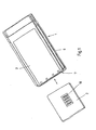
- the adapter 1 shown in Figure 1 has a housing whose dimensions correspond to those of a type II PCMCIA card.
- the housing 3 of the adapter 1 is provided on the right in Figure 1 located on the front side with a PCMCIA connection pad 8, which as seen in Figure 2 - completely housed in the housing 3.
- the housing 3 has at the terminal box 8 opposite end face an insertion slot 7 for a smart card 2, which merges into a laterally open receiving channel 6.
- the chip card 2 is provided with a flat contact field 18 and can be inserted or pulled out in the direction of the double arrow shown in the housing 3 of the adapter 1.
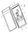
- the housing 3 of the adapter 1 consists of an upper cover plate 4 and a lower cover plate 5, which are connected to one another by a frame-shaped intermediate element 19.
- the cover plates 4 and 5 produced as stamped sheet metal parts have orthogonally angled staples 20 and 21, which ensures a simple but nevertheless reliable connection of the cover plates 4 and 5 with the intermediate element 19, which can be designed in several parts, despite different materials.
- That at the arranged lower cover plate intermediate member 19 is formed as a substantially U-shaped frame, whose legs on its inner contour clamping and guiding portions for receiving the circuit board 9 and the device 11 have.
- the intermediate element 19 in the region of the insertion slot 7 on an end face inlet bevel 22, which allows easy insertion of the smart card 2 in the receiving channel 6 of the adapter. Due to the frame-like configuration of the intermediate element 19, a high connection rigidity of the housing 3 of the adapter 1 is ensured.
- the circuit board 9 has a shortened in the extension direction of the receiving channel 6 relative to the receiving channel 6 length and is provided on the insertion slot 7 facing end with a device 11 for positioning the circuit board 9 and for guiding the smart card 2 in the receiving channel 6, wherein the device
- the plastic-made device 11 for positioning the printed circuit board 9 has two arm-shaped support elements 12 and two arm-shaped spring elements 13 with a fixed end and a free end which extends in the extension direction of the Receiving channels 6 extend parallel and perpendicular to the extension direction of the receiving channel 6 are spaced from each other.
- the free ends of the support members 12 and the spring elements 13 extend on opposite sides of the circuit board 9 in the direction of the pad 8, which is electrically and mechanically connected to the circuit board 9 via contact elements 23. Due to the floating reception of the printed circuit board 9 via the device 11, the printed circuit board length can be designed variably. By varying the thickness of the support members 12 in the extension direction of the receiving channel a height adjustment for positioning the circuit board in the receiving channel 6 is given, so that an adaptation to different thickness boards with the device 11 for positioning in the receiving channel 6 of the adapter 1 is given.
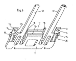
- the spring elements 13, as shown in Figures 4 and 7, in the region of its free end cams 14, which engage in corresponding holes of the shortened circuit board 9, as shown in Figure 9 can be seen.
- the spring elements 13 for positioning the circuit board strap-like guide means 15 which are aligned with the longitudinal sides of the circuit board 9, as can be seen in particular with reference to Figure 9.
- the in length compared to the Receiving channel 6 shortened circuit board 9 is clamped floating between the symmetrical to the front side parent support elements 12 and spring elements 13, wherein the support members 12 come to lie on the one and the spring elements 13 on the opposite side of the circuit board 9, as with reference to the figures 8, 9 and 10 to recognize.
- the spring elements 13 are positioned on the left and right of the contact elements 10 for contacting the contact pad 18 of a chip card 2.
- the so floating between the support members 12 and provided with cams 14 as locking means spring elements 13 floating mounted circuit board can compensate with the help of the device 11 position tolerances within the circuit board recording.
- the device 11 has to guide the chip card 2 arm-shaped spring elements 16 which extend in the direction of the pad 8 on the support elements 12 opposite side and are placed over the circuit board 9 to the contact elements 10, as shown in Figure 8 and 10 ,
- the spring elements 16 are arranged symmetrically to the front side of the circuit board.
- the ramp-like projection 17 and the projection 24 of the spring elements 13 are matched with respect to a touch contact with the smart card 2 in the leadership of the smart card 2 when inserting the smart card 2 in the receiving channel 6 such that the ramp-like projection 17 of the projection 24 of the spring elements 13 lags ,
- the projection 24 of the spring elements 13 in turn is formed lagging with respect to a touch contact with the chip card 2 of the establishment of the spring elements 16.
- the projection 17 and the spring elements 15 have a contact surface 25 or 26 for the front side of the printed circuit board 9, which serve for defined positioning of the printed circuit board 9 on the device 11.
Description
- Die Erfindung betrifft einen Adapter zum Kontaktieren von Chipkarten, insbesondere mit einem nach dem PCMCIA-Standard genormten Anschluß eines Datenverarbeitungsgerätes, mit einem steckkartenförmigen Gehäuse, welches einen an einer Stirnseite in einen Aufnahmekanal mündenden Einschubschlitz für die Aufnahme einer Chipkarte und ein an der gegenüberliegenden Stirnseite angeordnetes Anschlußfeld aufweist, und mit einer mit dem Anschlußfeld elektrisch verbundenen Leiterplatte, welche sich parallel zum Aufnahmekanal erstreckt und mit Kontaktelementen zum Kontaktieren der Chipkarte versehen ist.
- Unter einer Chipkarte im voranstehenden Sinne werden kartenförmige Trägerelemente elektronischer Bauteile, insbesondere von Mikroprozessoren, auf denen verschiedene abrufbare Informationen gespeichert werden können, verstanden. Derartige Chipkarten sind insbesondere im Bereich der Computertechnologie anzutreffen und erfreuen sich einer immer stärker werdenden Verbreitung im Zusammenhang mit der Authentifikation von Subjekten. Neben dieser Verwendung als Identitätskarte für z. B. die Bedienung von Zugangs-Kontrollsystemen, werden Chipkarten derzeit zunehmend auch im bargeldlosen Zahlungsverkehr eingesetzt, wo sie beispielsweise bei Kreditkarten oder im Rahmen von POS-Systemen die Magnetstreifenkarte ablösen.
- Zum Lesen einer Chipkarte sind als Kontaktiereinheit ausgebildete Lesegeräte bekannt, die in Form eines Adaptersystems es beispielsweise ermöglichen, eine Chipkarte an einen nach PCMCIA-Standard genormten Anschluß eines Datenverarbeitungssystems anzuschließen. Die im Stand der Technik hierzu bekannten Adapter weisen eine PCMCIA-Steckanschlußbuchse auf, die mit einem PCMCIA-Steckplatz des Datenverarbeitungssystems eine mechanische und elektrische Kontaktierung bewirkt. Das Auslesen der Chipkarte erfolgt dabei über im Aufnahmekanal für die Chipkarte angeordnete Kontaktelemente, welche dieselbe berührend oder, beispielsweise auf optischem oder magnetischem Weg, berührungslos kontaktieren.
- Ein Adapter zum Kontaktieren von Chipkarten ist beispielsweise aus der US 6,272,017 B1 bekannt. Der Adapter weist ein steckkartenförmiges Gehäuse mit einem an einer Stirnseite in einen Aufnahmekanal mündenden Einschubschlitz für die Aufnahme einer Chipkarte und einem an der gegenüberliegenden Stirnseite angeordneten Anschlußfeld auf. Mit dem Anschlußfeld ist eine Leiterplatte elektrisch verbunden, die sich parallel zum Aufnahmekanal erstreckt und mit Kontaktelementen zum Kontaktieren der Chipkarte versehen ist.
- Aus der DE 295 05 678 U1 ist eine Kontaktiereinheit für kartenförmige Trägerelemente elektronischer Baugruppen bekannt, die mit einer Basisplatte mit einer zur planparallelen Aufnahme eines kartenförmigen Trägerelementes geeigneten Größe, wenigstens einer im wesentlichen parallel zur Basisplatte angeordneten Leiterplatte mit Kontaktelementen für die elektronischen Baugruppen des Trägerelementes an ihrer Oberfläche sowie mit einem an einer Kante der Basisplatte angeordneten Anschlußfeld versehen ist. Ein zur Basisplatte im wesentlichen deckungsgleiches, plattenförmiges Abdeckelement bildet mit der Leiterplatte einen schlitzartigen Einschubkanal und ist im Bereich des Anschlußfeldes und der dieser gegenüberliegenden Ecken an der Basisplatte befestigt. Die Leiterplatte füllt aufgrund der Befestigung in dem Gehäuse den vollen Bauraum im Gehäuse aus.
- Die DE 295 05 678 U1 bildet den Oberbegriff des Patentanspruchs 1.
- Der Erfindung liegt die Aufgabe zugrunde, einen Adapter zum Kontaktieren von Chipkarten, insbesondere mit einem nach PCMCIA-Standard genormten Anschluß eines Datenverarbeitungsgerätes oder dergleichen, der eingangs genannten Art, dahingehend weiterzubilden, daß die wirtschaftlichen Vorteile einer höheren Bauteilintegration seitens der Leiterplattenfertigung nutzbar sind, so daß sich eine einfache und kostengünstige Herstellung erreichen läßt, die eine wirtschaftliche Massenproduktion insbesondere im Hinblick auf die zunehmend umfangreichere Verwendung vorgeschriebener Kartensysteme gewährleistet.
- Die Aufgabe ist bei einem Adapter der eingangs genannten Art erfindungsgemäß dadurch gelöst, daß die Leiterplatte in Erstreckungsrichtung des Aufnahmekanals eine gegenüber dem Aufnahmekanal verkürzte Länge aufweist und an der dem Einschubschlitz zugewandten Stirnseite mit einer Einrichtung zur Positionierung der Leiterplatte und zur Führung der Chipkarte in dem Aufnahmekanal versehen ist.
- Der Erfindung, die in den Ansprüchen definiert ist, liegt die Erkenntnis zugrunde, daß die Leiterplattenfläche reduziert werden muß, um die wirtschaftlichen Vorteile der höheren Baüteilintegration nutzen zu können. Diese Reduzierung bringt nicht nur eine Einsparung an Leiterplatten-Basismaterial, sondern auch eine Nutzensteigerung bei der Leiterplattenfertigung. Durch die erfindungsgemäße Einrichtung zur Positionierung der Leiterplatte und zur Führung der Chipkarte in dem Aufnahmekanal wird gleichzeitig das sichere Kontaktieren einer in den Aufnahmekanal eingeschobenen Chipkarte gewährleistet, so daß die beiden Kostenvorteile, die Einsparung von Leiterplatten-Basismaterial einerseits und die Nutzensteigerung bei der Leiterplattenfertigung andererseits, nutzbar sind.
- Ein solchermaßen ausgestalteter Adapter läßt sich einfach und kostengünstig herstellen und gestattet daher eine Massenproduktion im zuvor erwähnten Sinn. Dies ist darauf zurückzuführen, daß die vorteilhafterweise die Leiterplatte schwimmend einklemmende Einrichtung zum einen eine sichere Positionierung der verkürzten Leiterplatte in dem Aufnahmekanal des Gehäuses des Adapters und zum andern eine sichere Führung und Kontaktierung der Chipkarte in dem Aufnahmekanal des Gehäuses des Adapters zwischen Leiterplatte und oberer Abdeckplatte des Gehäuses des Adapters gewährleistet.
- Aus der US 5,846,092 ist ein Adapter für Speicherkarten bekannt, dessen steckkartenförmiges Gehäuse auf der einen Stirnseite einen Einschubschlitz zur Aufnahme einer Speicherkarte und auf der entgegengesetzten Stirnseite ein Anschlußfeld aufweist, das mit einer in dem Gehäuse angeordneten Leiterplatte elektrisch verbunden ist. Die Leiterplatte ist bei dem bekannten Adapter zwar kürzer ausgebildet als die Gesamtlänge des Gehäuses, jedoch wird die Speicherkarte nicht - wie bei der Erfindung - über bzw. unter die Leiterplatte geschoben, so daß sich die Kontaktfelder der Speicherkarte und der Leiterplatte flächig gegenüberliegen, sondern der Aufnahmekanal des Gehäuses ist derart angeordnet, daß die auszulesende Speicherkarte stimseitig zur Leiterplatte hingeführt und über Kontaktstifte ebenfalls stirnseitig kontaktiert wird.
- In einer bevorzugten Ausführungsform weist die Einrichtung zur Positionierung der Leiterplatte armförmige Tragelemente und armförmige Federelemente mit einem festen Ende und einem freien Ende auf, wobei die freien Enden der Tragelemente und der Federelemente auf einander gegenüber liegenden Seiten der Leiterplatte sich in Richtung des Anschlußfeldes erstrecken. Die armförmigen Tragelemente und Federelemente stellen so Funktionselemente für die Chipkartenführung und die Leiterplattenaufnahme bereit. Die Leiterplatte wird dabei zwischen den armförmigen Tragelementen und den armförmigen Federelementen schwimmend eingeklemmt. Dadurch, daß die Einrichtung mit der Leiterplatte direkt verbunden wird, ist die Leiterplattenlänge in Abhängigkeit der Anwendung ohne Änderungen an dem Gehäuse des Adapters oder des Aufnahmekanals variabel montierbar. Vorteilhafterweise werden anstelle von für PCMCIA-Adapter üblichen
- Leiterplattenlängen von etwa 75mm, entsprechend einer vollen Leiterplattenlänge, Leiterplatten mit einer Länge von bis zu 40mm verwendet.
- Vorteilhafterweise weisen die armförmigen Federelemente nockenförmige Rastmittel auf, welche in dazu korrespondierende an den Seiten der Leiterplatte vorgesehene Aufnahmen eingreifen. Die nockenförmigen Rastmittel sind vorteilhaft am freien Ende des Federelements angeordnet und die Aufnahmen sind in der Leiterplatte ausgebildete Löcher, vorzugsweise Fanglöcher, oder in der Leiterplatte ausgebildete Vertiefungen. Die Rastmittel gewährleisten eine sichere Verbindung zwischen der Leiterplatte und der Einrichtung.
- In einer weiteren vorteilhaften Ausgestaltung der Erfindung weisen die Federelemente Führungs- und/oder Anschlagsmittel zur Positionierung der Leiterplatte an der Einrichtung auf. Vorteilhafterweise sind die Führungsmittel als an den Federelementen angeordnete Laschen ausgebildet, welche mit den Längsseiten der Leiterplatte fluchten.
- In einer konkreten Ausgestaltung der Erfindung weist die Einrichtung zwei Tragelemente und zwei Federelemente auf, welche in Erstreckungsrichtung des Aufnahmekanals parallel und mit Abstand zueinander verlaufen und senkrecht zur Erstreckungsrichtung des Aufnahmekanals voneinander beabstandet sind. Vorteilhafterweise sind die Tragelemente und die Federelemente symmetrisch zur Stirnseite angeordnet, vorzugsweise derart, daß die Federelemente außen und die Tragelemente innen liegen, besonders bevorzugt derart, daß die Tragelemente links und rechts von den Kontaktelementen der Leiterplatte positionierbar sind.
- In einer weiteren vorteilhaften Ausgestaltung der Erfindung weisen die Arme der Federelemente in Erstreckungsrichtung des Aufnahmekanals eine zur Führung der Chipkarte dienende Auskragung auf.
- In einer weiteren Ausgestaltung der Erfindung weist die Einrichtung zur weiteren Führung der Chipkarte armförmige Federelemente auf, welche sich in Richtung des Anschlußfeldes erstrecken und über der Leiterplatte bis zu den Kontaktelementen aufgestellt sind. Vorteilhafterweise weist die Einrichtung des weiteren zwischen den Federelementen vorzugsweise mittig der Stirnseite der Leiterplatte, einen sich in Richtung des Anschlußfeldes erstreckenden rampenförmigen Vorsprung auf, welcher sich auf der den Tragelementen gegenüber liegenden Seite der Leiterplatte bis zu den Kontaktelementen der Leiterplatte erstreckt. Der rampenförmige Vorsprung eilt vorteilhaft hinsichtlich eines Berührungskontaktes mit der Chipkarte bei der Führung der Chipkarte der Auskragung der Rastmittel aufweisenden Federelemente nach.
- Eine weitere Ausgestaltung .der Erfindung sieht vor, daß die vorteilhafterweise aus Kunststoff bestehende Einrichtung einteilig ausgebildet ist, vorzugsweise als Kunststoff-Spritzgußteil.
- Weitere Einzelheiten, Merkmale und Vorteile der Erfindung werden nachfolgend anhand der in den Figuren dargestellten Ausführungsbeispiele näher erläutert. Dabei zeigen:
- Figur 1
- in einer perspektivischen Ansicht einen Adapter und eine Chipkarte;
- Figur 2
- in einer perspektivischen Ansicht den Adapter gemäß Fig. 1 mit abgehobener oberer Abdeckplatte;
- Figur 3
- in einer perspektivischen Ansicht eine Einrichtung zur Positionierung der Leiterplatte und zur Führung der Chipkarte in dem Aufnahmekanal des Adapters;
- Figur 4
- eine weitere perspektivische Ansicht der Einrichtung zur Positionierung der Leiterplatte und zur Führung der Chipkarte in dem Aufnahmekanal des Adapters;
- Figur 5
- eine Ansicht von oben auf die Einrichtung zur Positionierung der Leiterplatte und zur Führung der Chipkarte in dem Aufnahmekanal gemäß den Figuren 3 und 4;
- Figur 6
- eine Seitenansicht der Einrichtung zur Positionierung der Leiterplatte und zur Führung der Chipkarte in dem Aufnahmekanal;
- Figur 7
- eine Ansicht von unten auf die Einrichtung zur Positionierung der Leiterplatte und zur Führung der Chipkarte in dem Aufnahmekanal des Adapters;
- Figur 8
- eine perspektivische Ansicht von oben auf eine mit der Einrichtung zur Positionierung der Leiterplatte und zur Führung der Chipkarte in dem Aufnahmekanal des Adapters versehene Leiterplatte;
- Figur 9
- eine perspektivische Ansicht von unten auf eine mit der Einrichtung zur Positionierung der Leiterplatte und zur Führung der Chipkarte in dem Aufnahmekanal des Adapters versehene Leiterplatte und
- Figur 10
- eine Seitenansicht einer mit der Einrichtung zur Positionierung der Leiterplatte und zur Führung der Chipkarte in dem Aufnahmekanal des Adpaters versehene Leiterplatte.
- Der in Figur 1 dargestellte Adapter 1 weist ein Gehäuse auf, dessen Abmessungen denen einer PCMCIA-Steckkarte vom Typ II entsprechen. Das Gehäuse 3 des Adapters 1 ist an der in Figur 1 rechts gelegenen Stirnseite mit einem PCMCIA-Anschlußfeld 8 versehen, welches wie aus Figur 2 ersichtlich - vollkommen im Gehäuse 3 untergebracht ist. Das Gehäuse 3 weist an der dem Anschlußfeld 8 gegenüber liegenden Stirnseite einen Einschubschlitz 7 für eine Chipkarte 2 auf, der in einen seitlich offenen Aufnahmekanal 6 übergeht. Die Chipkarte 2 ist mit einem flächigen Kontaktfeld 18 versehen und läßt sich in Richtung des gezeigten Doppelpfeiles in das Gehäuse 3 des Adapters 1 einführen bzw. herausziehen.
- Wie aus Figur 2 ersichtlich ist, besteht das Gehäuse 3 des Adapters 1 aus einer oberen Abdeckplatte 4 und einer unteren Abdeckplatte 5, die durch ein rahmenförmiges Zwischenelement 19 miteinander verbunden sind. Die als Blechstanzteile gefertigten Abdeckplatten 4 und 5 weisen orthogonal abgewinkelte Krampen 20 und 21 auf, die eine einfache aber dennoch belastbare Verbindung der Abdeckplatten 4 und 5 mit dem Zwischenelement 19, welches mehrteilig ausgebildet sein kann, trotz Unterschiedlicher Materialien sicherstellt. Das an der unteren Abdeckplatte angeordnete Zwischenelement 19 ist als ein im wesentlichen U-förmiger Rahmen ausgebildet, dessen Schenkel an ihrer Innenkontur Klemm-und Führungsabschnitte zur Aufnahme der Leiterplatte 9 und der Einrichtung 11 aufweisen. Zum besseren Einführen der Chipkarte 2 weist das Zwischenelement 19 im Bereich des Einschubschlitzes 7 eine stimseitige Einlaufschräge 22 auf, die ein leichtes Einführen der Chipkarte 2 in den Aufnahmekanal 6 des Adapters ermöglicht. Durch die rahmenartige Ausgestaltung des Zwischenelements 19 ist eine hohe Verbindungssteifigkeit des Gehäuses 3 des Adapters 1 gewährleistet.
- Die Leiterplatte 9 weist eine in Erstreckungsrichtung des Aufnahmekanals 6 gegenüber dem Aufnahmekanal 6 verkürzte Länge auf und ist an der dem Einschubschlitz 7 zugewandten Stirnseite mit einer Einrichtung 11 zur Positionierung der Leiterplatte 9 und zur Führung der Chipkarte 2 in dem Aufnahmekanal 6 versehen, wobei die Einrichtung 11 die Leiterplatte 9 schwimmend einklemmt Wie in den Figuren 3 bis 10 dargestellt, weist die aus Kunststoff gefertigte Einrichtung 11 zur Positionierung der Leiterplatte 9 zwei armförmige Tragelemente 12 und zwei armförmige Federelemente 13 mit einem festen Ende und einem freien Ende auf, welche in Erstreckungsrichtung des Aufnahmekanals 6 parallel verlaufen und senkrecht zur Erstreckungsrichtung des Aufnahmekanals 6 von einander beabstandet sind. Die freien Enden der Tragelemente 12 und der Federelemente 13 erstrecken sich dabei auf einander gegenüber liegenden Seiten der Leiterplatte 9 in Richtung des Anschlußfeldes 8, welches mit der Leiterplatte 9 über Kontaktelemente 23 elektrisch und mechanisch verbunden ist. Durch die schwimmende Aufnahme der Leiterplatte 9 über die Einrichtung 11 ist die Leiterplattenlänge variabel gestaltbar. Durch Variation der Dicke der Tragelemente 12 in Erstreckungsrichtung des Aufnahmekanals ist eine Höhenanpassung zur Positionierung der Leiterplatte im Aufnahmekanal 6 gegeben, so daß eine Anpassung an unterschiedlich dicke Leiterplatten mit der Einrichtung 11 zur Positionierung im Aufnahmekanal 6 des Adapters 1 gegeben ist. Die Federelemente 13 weisen, wie in Figur 4 und 7 gezeigt, im Bereich ihres freien Endes Nocken 14 auf, welche in korrespondierende Löcher der verkürzten Leiterplatte 9 eingreifen, wie in Figur 9 zu erkennen. Weiter weisen die Federelemente 13 zur Positionierung der Leiterplatte laschenartige Führungsmittel 15 auf, welche mit den Längsseiten der Leiterplatte 9 fluchten, wie insbesondere anhand von Figur 9 zu erkennen. Die in ihrer Länge gegenüber dem Aufnahmekanal 6 verkürzte Leiterplatte 9 wird zwischen den symmetrisch zur Stirnseite angordneten Tragelementen 12 und Federelementen 13 schwimmend eingeklemmt, wobei die Tragelemente 12 auf der einen und die Federelemente 13 auf der gegenüber liegenden Seite der Leiterplatte 9 zu liegen kommen, wie anhand der Figuren 8, 9 und 10 zu erkennen. Die Federelemente 13 sind dabei links und rechts von den Kontaktelementen 10 zum Kontaktieren des Kontaktfeldes 18 einer Chipkarte 2 positioniert. Die so schwimmend zwischen den Tragelementen 12 und den mit Nocken 14 als Rastmittel versehenen Federelementen 13 schwimmend eingehängte Leiterplatte kann mit Hilfe der Einrichtung 11 Lagetoleranzen innerhalb der Leiterplattenaufnahme ausgleichen.
- Die Einrichtung 11 weist zur Führung der Chipkarte 2 armförmige Federelemente 16 auf, welche sich in Richtung des Anschlußfeldes 8 auf der den Tragelementen 12 gegenüber liegenden Seite erstrecken und über der Leiterplatte 9 bis zu den Kontaktelementen 10 aufgestellt sind, wie in Figur 8 und 10 dargestellt. Die Federelemente 16 sind dabei symmetrisch zur Stirnseite der Leiterplatte angeordnet. Weiter weist die Einrichtung 11 zwischen den Federelementen 16 mittig der Stirnseite der Leiterplatte 9 einen sich in Richtung des Anschlußfeldes 8 erstreckenden rampenförmigen Vorsprung 17 auf, welcher sich auf der den Tragelementen 12 gegenüber liegenden Seite der Leiterplatte 9 bis zu den Kontaktelementen 10 der Leiterplatte 9 erstreckt. Der rampenartige Vorsprung 17 und die Auskragung 24 der Federelemente 13 sind hinsichtlich eines Berührungskontaktes mit der Chipkarte 2 bei der Führung der Chipkarte 2 beim Einführen der Chipkarte 2 in den Aufnahmekanal 6 derart aufeinander abgestimmt, daß der rampenartige Vorsprung 17 der Auskragung 24 der Federelemente 13 nacheilt. Die Auskragung 24 der Federelemente 13 ihrerseits ist hinsichtlich eines Berührungskontaktes mit der Chipkarte 2 der Aufstellung der Federelemente 16 nacheilend ausgebildet.
- Wie anhand von Figur 8 und 9 zu erkennen, weisen der Vorsprung 17 und die Federelemente 15 eine Anlagefläche 25 bzw. 26 für die Stirnseite der Leiterplatte 9 auf, welche zur definierten Positionierung der Leiterplatte 9 an der Einrichtung 11 dienen.
- Die in den Figuren dargestellten Ausführungsbeispiele dienen lediglich der Erläuterung der Erfindung und sind für diese nicht beschränkend.
-
- 1
- Adapter
- 2
- Chipkarte
- 3
- Gehäuse
- 4
- obere Abdeckplatte
- 5
- untere Abdeckplatte
- 6
- Aufnahmekanal
- 7
- Einschubschlitz
- 8
- Anschlußfeld
- 9
- Leiterplatte
- 10
- Kontaktelemente
- 11
- Positionier- und Führungseinrichtung
- 12
- Tragelement
- 13
- Federelement
- 14
- Rastmittel (Nocken)
- 15
- Führungsmittel,
- 16
- Federelement
- 17
- Vorsprung (Rampe)
- 18
- Kontaktfeld
- 19
- Zwischenelement
- 20
- Krampen
- 21
- Krampen
- 22
- Einlaufschräge
- 23
- Kontaktelemente
- 24
- Auskragung
- 25
- Anlagefläche
- 26
- Anlagefläche
Claims (16)
- Adapter (1) zum Kontaktieren von Chipkarten (2), mit- einem steckkartenförmigen Gehäuse (3), welches einen an einer Stirnseite in einen Aufnahmekanal (6) mündenden Einschubschlitz (7) für die Aufnahme einer Chipkarte (2) und ein an der gegenüberliegenden Stirnseite angeordnetes Anschlußfeld (8) aufweist, und mit- einer mit dem Anschlußfeld (8) elektrisch verbundenen Leiterplatte (9), welche sich parallel zum Aufnahmekanal (6) erstreckt und mit Kontaktelementen (10) zum Kontaktieren der Chipkarte (2) versehen ist,dadurch gekennzeichnet, daß
die Leiterplatte (9) in Erstreckungsrichtung des Aufnahmekanals (6) kürzer ist als der Aufnahmekanal (6) und an der dem Einschubschlitz (7) zugewandten Stirnseite mit einer Einrichtung (11) zur Positionierung der Leiterplatte (9) und zur Führung der Chipkarte (2) in dem Aufnahmekanal (6) versehen ist. - Adapter nach Anspruch 1, dadurch gekennzeichnet, daß die Einrichtung (11) die Leiterplatte (9) mit Spiel einklemmt.
- Adapter nach Anspruch 1 oder Anspruch 2, dadurch gekennzeichnet, daß die Einrichtung (11) zur Positionierung der Leiterplatte (9) armförmige Tragelemente (12) und armförmige Federelemente (13) mit einem festen Ende und einem freien Ende aufweist, wobei die freien Enden der Tragelemente (12) .und der Federelemente (13) auf einander gegenüberliegenden Seiten der Leiterplatte (9) sich in Richtung des Anschlußfeldes (8) erstrecken.
- Adapter nach Anspruch 3, dadurch gekennzeichnet, daß die Federelemente (13) nockenförmige Rastmittel (14) aufweisen, welche in dazu korrespondierende auf der Leiterplatte (9) vorgesehene Aufnahmen eingreifen.
- Adapter nach Anspruch 4, dadurch gekennzeichnet, daß die Rastmittel (14) am freien Ende des Federelements (13) angeordnet sind.
- Adapter nach Anspruch 4 oder Anspruch 5, dadurch gekennzeichnet, daß die Aufnahmen in der Leiterplatte (9) ausgebildete Löcher, vorzugsweise Fanglöcher, sind.
- Adapter nach Anspruch 4 oder Anspruch 5, dadurch gekennzeichnet, daß die Aufnahmen in der Leiterplatte (9) ausgebildete Vertiefungen sind.
- Adapter nach einem der Ansprüche 3 bis 7, dadurch gekennzeichnet, daß die Federelemente (13) Führungsmittel (15) zur Positionierung der Leiterplatte (9) an der Einrichtung (11) aufweisen.
- Adapter nach einem der Ansprüche 3 bis 8, dadurch gekennzeichnet, daß die Einrichtung (11) zwei Tragelemente (12) und zwei Federelemente (13) aufweist, welche in Aufnahmekanalerstreckungsrichtung vorzugsweise parallel zueinander und mit Abstand zueinander verlaufen und senkrecht zur Aufnahmekanalerstreckungsrichtung voneinander beabstandet sind.
- Adapter nach Anspruch 9, dadurch gekennzeichnet, daß die Tragelemente (12) und die Federelemente (13) symmetrisch zur Stirnseite angeordnet sind, vorzugsweise derart, daß die Federelemente (13) außen und die Tragelemente (12) innen liegen, besonders bevorzugt derart, daß die Tragelemente (12) links und rechts von den Kontaktelementen (10) der Leiterplatte (9) positionierbar sind.
- Adapter nach einem der Ansprüche 3 bis 10, dadurch gekennzeichnet, daß der Arm der Federelemente (13) in Aufnahmekanalerstreckungsrichtung eine zur Führung der Chipkarte (2) dienende Auskragung (24) aufweist.
- Adapter nach einem der Ansprüche 1 bis 11, dadurch gekennzeichnet, daß die Einrichtung (11) zur Führung der Chipkarte (2) armförmige Federelemente (16) aufweist, welche sich in Richtung des Anschlußfeldes (8) erstrecken und über der Leiterplatte (9) bis zu den Kontaktelementen (10) aufgestellt sind.
- Adapter nach Anspruch 12, dadurch gekennzeichnet, daß die Einrichtung (11) zwischen den Federelementen (16), vorzugsweise mittig der Stirnseite der Leiterplatte (9), einen sich in Richtung des Anschlußfeldes (8) erstreckenden rampenartigen Vorsprung (17) aufweist, welcher sich auf der den Tragelementen (12) gegenüberliegenden Seite der Leiterplatte (9) bis zu den Kontaktelementen (10) der Leiterplatte (9) erstreckt.
- Adapter nach Anspruch 13, dadurch gekennzeichnet, daß der rampenartige Vorsprung (17) hinsichtlich eines Kontaktes mit der Chipkarte (2) bei der Führung der Chipkarte (2) der Auskragung (24) und der Aufstellung der Federelemente (16) nacheilt.
- Adapter nach einem der Ansprüche 1 bis 14, dadurch gekennzeichnet, daß die Einrichtung (11) einteilig ausgebildet ist.
- Adapter nach einem der Ansprüche 1 bis 15, dadurch gekennzeichnet, daß die Einrichtung (11) aus Kunststoff ist, vorzugsweise ein Kunststoff-Spritzgußteil.
Applications Claiming Priority (3)
| Application Number | Priority Date | Filing Date | Title |
|---|---|---|---|
| DE20117188U | 2001-10-19 | ||
| DE20117188U DE20117188U1 (de) | 2001-10-19 | 2001-10-19 | Adapter zum Kontaktieren von Chipkarten |
| PCT/EP2002/011558 WO2003036551A1 (de) | 2001-10-19 | 2002-10-16 | Adapter zum kontaktieren von chipkarten |
Publications (2)
| Publication Number | Publication Date |
|---|---|
| EP1436765A1 EP1436765A1 (de) | 2004-07-14 |
| EP1436765B1 true EP1436765B1 (de) | 2006-11-15 |
Family
ID=7963064
Family Applications (1)
| Application Number | Title | Priority Date | Filing Date |
|---|---|---|---|
| EP02801891A Expired - Lifetime EP1436765B1 (de) | 2001-10-19 | 2002-10-16 | Adapter zum kontaktieren von chipkarten |
Country Status (7)
| Country | Link |
|---|---|
| US (1) | US6967848B2 (de) |
| EP (1) | EP1436765B1 (de) |
| JP (1) | JP2005506638A (de) |
| AT (1) | ATE345541T1 (de) |
| DE (2) | DE20117188U1 (de) |
| NO (1) | NO20032646L (de) |
| WO (1) | WO2003036551A1 (de) |
Families Citing this family (8)
| Publication number | Priority date | Publication date | Assignee | Title |
|---|---|---|---|---|
| DE102004013320A1 (de) * | 2004-03-17 | 2005-09-29 | Giesecke & Devrient Gmbh | Vorrichtung zum Verbinden einer Smart Card mit einem USB-Anschluss |
| US7040905B1 (en) * | 2005-05-18 | 2006-05-09 | Epo Science & Technology Inc. | Structure for combining printing circuit board with rack |
| US7097511B1 (en) * | 2005-07-21 | 2006-08-29 | Research In Motion Limited | Structure for SIM card assembly and disassembly |
| DE102005061688A1 (de) * | 2005-12-21 | 2007-07-05 | Stocko Contact Gmbh & Co. Kg | Kontaktiereinheit |
| ATE544326T1 (de) * | 2007-12-03 | 2012-02-15 | Osram Ag | Gehäuse für elektrische komponenten |
| US9136621B1 (en) * | 2012-08-14 | 2015-09-15 | Ciena Corporation | Guides and tab arrangement to retain a card having an edge connector and method of use |
| JP2014085936A (ja) * | 2012-10-25 | 2014-05-12 | Toshiba Corp | 電子機器 |
| TWM459640U (zh) * | 2013-04-09 | 2013-08-11 | Chi Mei Comm Systems Inc | 晶片卡裝取結構及具有該晶片卡裝取結構之電子裝置 |
Citations (3)
| Publication number | Priority date | Publication date | Assignee | Title |
|---|---|---|---|---|
| DE3902230A1 (de) * | 1989-01-26 | 1990-08-02 | Daimler Benz Ag | Einrichtung zur befestigung eines elektrischen moduls an einem basisteil |
| DE4310517A1 (de) * | 1993-03-31 | 1994-10-06 | Wolfgang Neifer | Vorrichtung zum Lesen von Chipkarten |
| DE19533569A1 (de) * | 1995-09-11 | 1997-03-13 | Ibm | Vorrichtung zur Herstellung einer Verbindung mit einer Leiterplatte |
Family Cites Families (8)
| Publication number | Priority date | Publication date | Assignee | Title |
|---|---|---|---|---|
| US5457601A (en) * | 1993-12-08 | 1995-10-10 | At&T Corp. | Credit card-sized modem with modular DAA |
| DE29505678U1 (de) | 1995-04-01 | 1995-06-14 | Stocko Metallwarenfab Henkels | Kontaktiereinheit für kartenförmige Trägerelemente |
| US5846092A (en) * | 1997-08-05 | 1998-12-08 | Minnesota Mining And Manufacturing Company | Plastic cased IC card adapter assembly |
| DE29722142U1 (de) * | 1997-12-16 | 1998-02-12 | Stocko Metallwarenfab Henkels | Adapter zum Kontaktieren von Chipkarten |
| JP3017709B2 (ja) * | 1998-01-22 | 2000-03-13 | ティーディーケイ株式会社 | カード保持体 |
| US6015092A (en) * | 1998-02-05 | 2000-01-18 | Postlewaite; William M. | Smart card reader having angled smart card holder |
| US6075709A (en) * | 1998-07-08 | 2000-06-13 | Yang; Li-Ho | Memory adapter |
| DE19925146C2 (de) * | 1999-06-02 | 2003-01-09 | Itt Mfg Enterprises Inc | Steckkarte für elektronische Geräte |
-
2001
- 2001-10-19 DE DE20117188U patent/DE20117188U1/de not_active Expired - Lifetime
-
2002
- 2002-10-16 JP JP2003538967A patent/JP2005506638A/ja active Pending
- 2002-10-16 DE DE50208726T patent/DE50208726D1/de not_active Expired - Fee Related
- 2002-10-16 WO PCT/EP2002/011558 patent/WO2003036551A1/de active IP Right Grant
- 2002-10-16 EP EP02801891A patent/EP1436765B1/de not_active Expired - Lifetime
- 2002-10-16 AT AT02801891T patent/ATE345541T1/de not_active IP Right Cessation
- 2002-10-16 US US10/490,078 patent/US6967848B2/en not_active Expired - Fee Related
-
2003
- 2003-06-11 NO NO20032646A patent/NO20032646L/no not_active Application Discontinuation
Patent Citations (3)
| Publication number | Priority date | Publication date | Assignee | Title |
|---|---|---|---|---|
| DE3902230A1 (de) * | 1989-01-26 | 1990-08-02 | Daimler Benz Ag | Einrichtung zur befestigung eines elektrischen moduls an einem basisteil |
| DE4310517A1 (de) * | 1993-03-31 | 1994-10-06 | Wolfgang Neifer | Vorrichtung zum Lesen von Chipkarten |
| DE19533569A1 (de) * | 1995-09-11 | 1997-03-13 | Ibm | Vorrichtung zur Herstellung einer Verbindung mit einer Leiterplatte |
Also Published As
| Publication number | Publication date |
|---|---|
| JP2005506638A (ja) | 2005-03-03 |
| WO2003036551A8 (de) | 2003-12-24 |
| NO20032646D0 (no) | 2003-06-11 |
| DE20117188U1 (de) | 2002-01-03 |
| DE50208726D1 (de) | 2006-12-28 |
| NO20032646L (no) | 2003-07-29 |
| WO2003036551A1 (de) | 2003-05-01 |
| EP1436765A1 (de) | 2004-07-14 |
| ATE345541T1 (de) | 2006-12-15 |
| US6967848B2 (en) | 2005-11-22 |
| US20040243748A1 (en) | 2004-12-02 |
Similar Documents
| Publication | Publication Date | Title |
|---|---|---|
| EP0924640B1 (de) | Adapter zum Kontaktieren von Chipkarten | |
| EP0866413B1 (de) | Adapter für die Kontaktierung von kartenförmigen Trägerelementen | |
| EP0775964B1 (de) | Kontaktiereinheit für kartenförmige Trägerelemente elektronischer Baugruppen | |
| EP1418528B1 (de) | Chipkartenleser | |
| EP0735507B1 (de) | Kontaktiereinheit für kartenförmige Trägerelemente | |
| DE60220480T2 (de) | Kartenverbinderseinrichtung für verschiede Kartentypen | |
| DE69837176T2 (de) | Datenkartengehäuse | |
| DE19846366C2 (de) | Steckkarte für elektronische Geräte | |
| DE19947162C1 (de) | Steckkarte für elektronische Geräte | |
| DE4310517C2 (de) | Vorrichtung zum Lesen von Chipkarten | |
| EP1056032B1 (de) | Chipkartenleser | |
| DE10038287A1 (de) | Steckkarte für elektronische Geräte | |
| EP1008280A1 (de) | Kontaktiereinheit für ein kartenförmiges trägerelement elektronischer baugruppen, insbesondere nach pcmcia-norm | |
| EP1512111A1 (de) | Chipkartenleser im pc kartenformat | |
| DE69937103T2 (de) | Tragbare Chipkarten-Leseanordnung | |
| EP1436765B1 (de) | Adapter zum kontaktieren von chipkarten | |
| DE10151205A1 (de) | Kartenverbindungseinrichtung | |
| DE102018109251B4 (de) | Baugruppe mit einer Leitungsklemme aufweisend eine flächige Antenne und Leuchtenbaugruppe | |
| DE19925076B4 (de) | Doppel-SIM-Kartenleser | |
| DE19815549C2 (de) | Steckkarte für elektronische Geräte | |
| DE102004032104B4 (de) | Kontaktiereinheit zum Lesen und/oder Beschreiben von Chipkarten | |
| DE19704503C1 (de) | Steckverbindung für einen Stapel kartenförmiger Datenträgeranordnungen | |
| EP1610261A1 (de) | Chipmodul für einen tragbaren Datenträger | |
| WO1998033143A1 (de) | Trägerelement zum einbau in kombi-chipkarten und kombi-chipkarte | |
| DE3840663A1 (de) | Kartenlesevorrichtung |
Legal Events
| Date | Code | Title | Description |
|---|---|---|---|
| PUAI | Public reference made under article 153(3) epc to a published international application that has entered the european phase |
Free format text: ORIGINAL CODE: 0009012 |
|
| 17P | Request for examination filed |
Effective date: 20040226 |
|
| AK | Designated contracting states |
Kind code of ref document: A1 Designated state(s): AT BE BG CH CY CZ DE DK EE ES FI FR GB GR IE IT LI LU MC NL PT SE SK TR |
|
| 17Q | First examination report despatched |
Effective date: 20040830 |
|
| GRAP | Despatch of communication of intention to grant a patent |
Free format text: ORIGINAL CODE: EPIDOSNIGR1 |
|
| GRAS | Grant fee paid |
Free format text: ORIGINAL CODE: EPIDOSNIGR3 |
|
| GRAA | (expected) grant |
Free format text: ORIGINAL CODE: 0009210 |
|
| AK | Designated contracting states |
Kind code of ref document: B1 Designated state(s): AT BE BG CH CY CZ DE DK EE ES FI FR GB GR IE IT LI LU MC NL PT SE SK TR |
|
| PG25 | Lapsed in a contracting state [announced via postgrant information from national office to epo] |
Ref country code: SK Free format text: LAPSE BECAUSE OF FAILURE TO SUBMIT A TRANSLATION OF THE DESCRIPTION OR TO PAY THE FEE WITHIN THE PRESCRIBED TIME-LIMIT Effective date: 20061115 Ref country code: IT Free format text: LAPSE BECAUSE OF FAILURE TO SUBMIT A TRANSLATION OF THE DESCRIPTION OR TO PAY THE FEE WITHIN THE PRESCRIBED TIME-LIMIT;WARNING: LAPSES OF ITALIAN PATENTS WITH EFFECTIVE DATE BEFORE 2007 MAY HAVE OCCURRED AT ANY TIME BEFORE 2007. THE CORRECT EFFECTIVE DATE MAY BE DIFFERENT FROM THE ONE RECORDED. Effective date: 20061115 Ref country code: FI Free format text: LAPSE BECAUSE OF FAILURE TO SUBMIT A TRANSLATION OF THE DESCRIPTION OR TO PAY THE FEE WITHIN THE PRESCRIBED TIME-LIMIT Effective date: 20061115 Ref country code: CZ Free format text: LAPSE BECAUSE OF FAILURE TO SUBMIT A TRANSLATION OF THE DESCRIPTION OR TO PAY THE FEE WITHIN THE PRESCRIBED TIME-LIMIT Effective date: 20061115 Ref country code: IE Free format text: LAPSE BECAUSE OF FAILURE TO SUBMIT A TRANSLATION OF THE DESCRIPTION OR TO PAY THE FEE WITHIN THE PRESCRIBED TIME-LIMIT Effective date: 20061115 Ref country code: NL Free format text: LAPSE BECAUSE OF FAILURE TO SUBMIT A TRANSLATION OF THE DESCRIPTION OR TO PAY THE FEE WITHIN THE PRESCRIBED TIME-LIMIT Effective date: 20061115 |
|
| REG | Reference to a national code |
Ref country code: GB Ref legal event code: FG4D Free format text: NOT ENGLISH |
|
| REG | Reference to a national code |
Ref country code: CH Ref legal event code: EP |
|
| REF | Corresponds to: |
Ref document number: 50208726 Country of ref document: DE Date of ref document: 20061228 Kind code of ref document: P |
|
| REG | Reference to a national code |
Ref country code: IE Ref legal event code: FG4D Free format text: LANGUAGE OF EP DOCUMENT: GERMAN |
|
| GBT | Gb: translation of ep patent filed (gb section 77(6)(a)/1977) |
Effective date: 20070111 |
|
| PG25 | Lapsed in a contracting state [announced via postgrant information from national office to epo] |
Ref country code: SE Free format text: LAPSE BECAUSE OF FAILURE TO SUBMIT A TRANSLATION OF THE DESCRIPTION OR TO PAY THE FEE WITHIN THE PRESCRIBED TIME-LIMIT Effective date: 20070215 Ref country code: BG Free format text: LAPSE BECAUSE OF FAILURE TO SUBMIT A TRANSLATION OF THE DESCRIPTION OR TO PAY THE FEE WITHIN THE PRESCRIBED TIME-LIMIT Effective date: 20070215 Ref country code: DK Free format text: LAPSE BECAUSE OF FAILURE TO SUBMIT A TRANSLATION OF THE DESCRIPTION OR TO PAY THE FEE WITHIN THE PRESCRIBED TIME-LIMIT Effective date: 20070215 |
|
| PG25 | Lapsed in a contracting state [announced via postgrant information from national office to epo] |
Ref country code: ES Free format text: LAPSE BECAUSE OF FAILURE TO SUBMIT A TRANSLATION OF THE DESCRIPTION OR TO PAY THE FEE WITHIN THE PRESCRIBED TIME-LIMIT Effective date: 20070226 |
|
| PG25 | Lapsed in a contracting state [announced via postgrant information from national office to epo] |
Ref country code: PT Free format text: LAPSE BECAUSE OF FAILURE TO SUBMIT A TRANSLATION OF THE DESCRIPTION OR TO PAY THE FEE WITHIN THE PRESCRIBED TIME-LIMIT Effective date: 20070416 |
|
| ET | Fr: translation filed | ||
| NLV1 | Nl: lapsed or annulled due to failure to fulfill the requirements of art. 29p and 29m of the patents act | ||
| REG | Reference to a national code |
Ref country code: IE Ref legal event code: FD4D |
|
| PLBE | No opposition filed within time limit |
Free format text: ORIGINAL CODE: 0009261 |
|
| STAA | Information on the status of an ep patent application or granted ep patent |
Free format text: STATUS: NO OPPOSITION FILED WITHIN TIME LIMIT |
|
| 26N | No opposition filed |
Effective date: 20070817 |
|
| BERE | Be: lapsed |
Owner name: STOCKO CONTACT G.M.B.H. & CO. KG Effective date: 20071031 |
|
| PG25 | Lapsed in a contracting state [announced via postgrant information from national office to epo] |
Ref country code: GR Free format text: LAPSE BECAUSE OF FAILURE TO SUBMIT A TRANSLATION OF THE DESCRIPTION OR TO PAY THE FEE WITHIN THE PRESCRIBED TIME-LIMIT Effective date: 20070216 |
|
| PG25 | Lapsed in a contracting state [announced via postgrant information from national office to epo] |
Ref country code: MC Free format text: LAPSE BECAUSE OF NON-PAYMENT OF DUE FEES Effective date: 20071031 |
|
| REG | Reference to a national code |
Ref country code: CH Ref legal event code: PL |
|
| PG25 | Lapsed in a contracting state [announced via postgrant information from national office to epo] |
Ref country code: LI Free format text: LAPSE BECAUSE OF NON-PAYMENT OF DUE FEES Effective date: 20071031 Ref country code: CH Free format text: LAPSE BECAUSE OF NON-PAYMENT OF DUE FEES Effective date: 20071031 |
|
| PG25 | Lapsed in a contracting state [announced via postgrant information from national office to epo] |
Ref country code: BE Free format text: LAPSE BECAUSE OF NON-PAYMENT OF DUE FEES Effective date: 20071031 |
|
| PG25 | Lapsed in a contracting state [announced via postgrant information from national office to epo] |
Ref country code: EE Free format text: LAPSE BECAUSE OF FAILURE TO SUBMIT A TRANSLATION OF THE DESCRIPTION OR TO PAY THE FEE WITHIN THE PRESCRIBED TIME-LIMIT Effective date: 20061115 |
|
| PGFP | Annual fee paid to national office [announced via postgrant information from national office to epo] |
Ref country code: DE Payment date: 20081105 Year of fee payment: 7 |
|
| PGFP | Annual fee paid to national office [announced via postgrant information from national office to epo] |
Ref country code: AT Payment date: 20081015 Year of fee payment: 7 |
|
| PGFP | Annual fee paid to national office [announced via postgrant information from national office to epo] |
Ref country code: FR Payment date: 20081014 Year of fee payment: 7 |
|
| PGFP | Annual fee paid to national office [announced via postgrant information from national office to epo] |
Ref country code: GB Payment date: 20081021 Year of fee payment: 7 |
|
| PG25 | Lapsed in a contracting state [announced via postgrant information from national office to epo] |
Ref country code: LU Free format text: LAPSE BECAUSE OF NON-PAYMENT OF DUE FEES Effective date: 20071016 Ref country code: CY Free format text: LAPSE BECAUSE OF FAILURE TO SUBMIT A TRANSLATION OF THE DESCRIPTION OR TO PAY THE FEE WITHIN THE PRESCRIBED TIME-LIMIT Effective date: 20061115 |
|
| PG25 | Lapsed in a contracting state [announced via postgrant information from national office to epo] |
Ref country code: TR Free format text: LAPSE BECAUSE OF FAILURE TO SUBMIT A TRANSLATION OF THE DESCRIPTION OR TO PAY THE FEE WITHIN THE PRESCRIBED TIME-LIMIT Effective date: 20061115 |
|
| REG | Reference to a national code |
Ref country code: FR Ref legal event code: ST Effective date: 20100630 |
|
| PG25 | Lapsed in a contracting state [announced via postgrant information from national office to epo] |
Ref country code: FR Free format text: LAPSE BECAUSE OF NON-PAYMENT OF DUE FEES Effective date: 20091102 Ref country code: DE Free format text: LAPSE BECAUSE OF NON-PAYMENT OF DUE FEES Effective date: 20100501 |
|
| PG25 | Lapsed in a contracting state [announced via postgrant information from national office to epo] |
Ref country code: AT Free format text: LAPSE BECAUSE OF NON-PAYMENT OF DUE FEES Effective date: 20091016 |
|
| PG25 | Lapsed in a contracting state [announced via postgrant information from national office to epo] |
Ref country code: GB Free format text: LAPSE BECAUSE OF NON-PAYMENT OF DUE FEES Effective date: 20091016 |