EP1420448A1 - Teststruktur zur Bestimmung der elektrischen Belastbarkeit von Kontakten - Google Patents
Teststruktur zur Bestimmung der elektrischen Belastbarkeit von Kontakten Download PDFInfo
- Publication number
- EP1420448A1 EP1420448A1 EP03023382A EP03023382A EP1420448A1 EP 1420448 A1 EP1420448 A1 EP 1420448A1 EP 03023382 A EP03023382 A EP 03023382A EP 03023382 A EP03023382 A EP 03023382A EP 1420448 A1 EP1420448 A1 EP 1420448A1
- Authority
- EP
- European Patent Office
- Prior art keywords
- interconnects
- test structure
- dummy
- structure according
- test
- Prior art date
- Legal status (The legal status is an assumption and is not a legal conclusion. Google has not performed a legal analysis and makes no representation as to the accuracy of the status listed.)
- Granted
Links
Images

Classifications
-
- H—ELECTRICITY
- H10—SEMICONDUCTOR DEVICES; ELECTRIC SOLID-STATE DEVICES NOT OTHERWISE PROVIDED FOR
- H10P—GENERIC PROCESSES OR APPARATUS FOR THE MANUFACTURE OR TREATMENT OF DEVICES COVERED BY CLASS H10
- H10P74/00—Testing or measuring during manufacture or treatment of wafers, substrates or devices
- H10P74/27—Structural arrangements therefor
- H10P74/277—Circuits for electrically characterising or monitoring manufacturing processes, e.g. circuits in tested chips or circuits in testing wafers
Definitions
- the invention relates to a test structure for determining the electrical resilience of contacts, especially of electrical connections between one another Interconnects through vias arranged in contact holes on one Test chip.
- test structures in the form of geometric shapes for example Structures developed with the help of defects within can be reliably detected over a large area.
- the bond pad configurations are used for contacting for test purposes usual standard chips used.
- This Test structures are on test chips in small numbers manufactured in parallel with the actual production and then subjected to appropriate test procedures. It did turned out to be cheap if the test chips at the same time with the actual chips to be produced on the same Wafers are arranged and thus the same production process run through.
- test structures are so-called square test structures in the form of a 3D or 2D matrix, so that basically also errors in vertical structures (vias) can be detected. It is particularly important here at Product or technology qualification, especially testing the electrical resilience of the vias between the metal levels. With the help of special acceleration processes can then make a statement about the maximum current or Dielectric strength stating a maximum lifetime and operating temperature.
- the so-called “downstream” or “upstream structures, ie vias with corresponding Current direction, the critical transition in each case (via on metal track) can be realized with minimal overlap. This is usually the area of the landing pads, i.e. real ones Chips the contact area between two metal levels where one or more vias are placed. It can be used in one Test structure of the so-called “worst case” are simulated, i.e. that when arranging the contacts and the chosen one Overlaps in the test structure to test the worst Case is assumed.
- the invention is therefore based on the object of a test structure to determine the electrical load capacity of Generate transitions between metal tracks with the on simple way a high to very high occupancy for the worst case can be tested.
- the problem underlying the invention is in solved a test structure of the type mentioned in the beginning, that around the contact hole inside the top one and / or the underlying interconnect level Structures are arranged adjacent to each other with a predetermined distance are.
- the additional structures are a continuation of the invention as dummy structures with or without any circuitry Function trained, which is dummy or can act electrically active interconnects.
- At least a dummy interconnect is arranged around the contact hole, which prevents any uncontrolled expansion and a minimum of coverage is ensured, as in the Circuit layout specified according to the design rules.
- interconnects of the corresponding interconnect level and the dummy interconnects in the same interconnect level consist of the same material, e.g. Metal, aluminum or polysilicon.
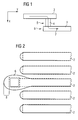
- FIG. 1 shows a schematic representation of a test structure 1 with an interconnect 2 of the metallization level 3 (Me3) and an interconnect 3 of the metallization level above (Me4) via a via 4 in a contact hole 5 electrically connected to one another between the two interconnects 2, 3 are.
- the transition is the critical edge 6 from Via 4 to Leitbahn 2 (in the case of a Downstream structure).
- an "upstream structure” would be the critical edge (not shown) analogously to the Crossing from Via 4 to Leitbahn 3.
- Arrow 7 shows the direction of current flow. This current flow (arrow 7) leads to a degeneration of the lower interconnect 2 (with upstream the upper orbit), which is until the contact between Via 4 and Leitbahn 2 can lead.
- the downtime depends on it structure-related from the overlap of the contact surface of the contact with the interconnect in the area of the critical edge 6 from, the minimum overlap over technology-defined Design rules is defined.
- the metallization aimed at by the necessary wiring be set as close as possible in the circuit layout, in order to minimize the chip area, whereby in this case the overlap from lane 2 to via 4 is minimal is drawn.
- test structures 1 through the implementation of a so-called “nested” environment with the help of dummy traces 9 um route 2 and vias 4 (critical structure) are secure can be prevented (Fig. 3).
- the metal, e.g. Al, Cu, existing Dummy traces 9 meet for what is described here
- Example of a test structure no electrical purpose, but "simulate” only a maximum occupancy density the critical structure. This maximum occupancy density corresponds then the real conditions in the product as well as that critical case of minimal overlap (“worst case"). It it is understood that from electrically active orbits neighboring Structures for the test structure can be used as dummies can.
- Fig. 4 shows a schematic cross section through an inventive Test structure 1, in the in the metallization level 3 (Me3) a "nested" structure with dummy interconnects 9 is shown.
Landscapes
- Internal Circuitry In Semiconductor Integrated Circuit Devices (AREA)
- Testing Or Measuring Of Semiconductors Or The Like (AREA)
- Design And Manufacture Of Integrated Circuits (AREA)
Abstract
Description
- Fig.1:
- einen schematischen Querschnitt von übereinander liegenden Leitbahnen (Metallisierungsebene 3 / Me3) und Metallisierungsebene 4 /Me4) und ein diese über ein Kontaktloch verbindendes Via als "Downstream Struktur";
- Fig. 2:
- eine schematische Darstellung der Leitbahnen der Metallisierungsebene 3 (Me3) mit verfälschten Struktureigenschaften infolge der Aufweitung der Leitbahn dieser Metallisierungsebene;
- Fig. 3:
- eine schematische Darstellung der Metallisierungsebene 3 mit erfindungsgemäß um die aktive Leitbahn herum angeordneten Dummy-Leitbahnen; und
- Fig. 4:
- eine schematische Schnittdarstellung der Anordnung nach Fig. 3.
- 1
- Teststruktur
- 2
- Leitbahn
- 3
- Leitbahn
- 4
- Via
- 5
- Kontaktloch
- 6
- kritische Kante
- 7
- Pfeil (Stromflussrichtung)
- 8
- Aufweitung
- 9
- Dummy-Leitbahn
- 10
- Minimum an Überdeckung 10
- Me3
- Metallisierungsebene 3
- Me4
- Metallisierungsebene 4
Claims (9)
- Teststruktur zur Bestimmung der elektrischen Belastbarkeit von Kontakten, insbesondere von elektrischen Verbindungen zwischen übereinander angeordneten Leitbahnen durch in Kontaktlöchern angeordnete Vias auf einem Testchip, dadurch gekennzeichnet, dass um das Via (4) bzw. Kontaktloch (5) und die zugehörige Leitbahn (2; 3) herum innerhalb der obersten und/oder der darunter liegenden Leitbahn (2, 3) der Metallisierungsebene (Me3) oder (Me4) ebene zusätzliche Strukturen dicht benachbart angeordnet sind.
- Teststruktur nach Anspruch 1, dadurch gekennzeichnet, dass die zusätzlichen Strukturen als Dummy-Strukturen mit oder ohne jede schaltungstechnische Funktion ausgebildet sind.
- Teststruktur nach Anspruch 1 und 2, dadurch gekennzeichnet, dass die zusätzlichen Strukturen Dummy-Leitbahnen (9) sind.
- Teststruktur nach Anspruch 3, dadurch gekennzeichnet, dass wenigstens eine Dummy-Leitbahn (9) um das Via (4) bzw. das Kontaktloch (5) herum angeordnet sind.
- Teststruktur nach Anspruch 4, dadurch gekennzeichnet, dass die Dummy-Leitbahnen (9) das Via (4) bzw. Kontaktloch (5) im wesentlichen äquidistant umgeben.
- Teststruktur nach einem der Ansprüche 1 bis 5, dadurch gekennzeichnet, dass die Leitbahnen (2, 3) der entsprechenden Metallisierungsebene und die Dummy-Leitbahnen (9) in der gleichen Metallisierungsebene aus dem gleichen Material bestehen.
- Teststruktur nach Anspruch 6, dadurch gekennzeichnet, dass die Leitbahnen (2, 3) und die Dummy-Leitbahnen (9) aus Metall bestehen.
- Teststruktur nach Anspruch 6, dadurch gekennzeichnet, dass die Leitbahnen (2, 3) und die Dummy-Leitbahnen (9) aus Aluminium bestehen.
- Teststruktur nach Anspruch 6, dadurch gekennzeichnet, dass die Leitbahnen (2, 3) und die Dummy-Leitbahnen (9) aus Polysilizium bestehen.
Applications Claiming Priority (2)
| Application Number | Priority Date | Filing Date | Title |
|---|---|---|---|
| DE10253626 | 2002-11-15 | ||
| DE10253626A DE10253626A1 (de) | 2002-11-15 | 2002-11-15 | Teststruktur zur Bestimmung der elektrischen Belastbarkeit von Kontakten |
Publications (2)
| Publication Number | Publication Date |
|---|---|
| EP1420448A1 true EP1420448A1 (de) | 2004-05-19 |
| EP1420448B1 EP1420448B1 (de) | 2006-08-09 |
Family
ID=32115563
Family Applications (1)
| Application Number | Title | Priority Date | Filing Date |
|---|---|---|---|
| EP03023382A Expired - Lifetime EP1420448B1 (de) | 2002-11-15 | 2003-10-16 | Teststruktur zur Bestimmung der elektrischen Belastbarkeit von Kontakten |
Country Status (3)
| Country | Link |
|---|---|
| US (1) | US6899543B2 (de) |
| EP (1) | EP1420448B1 (de) |
| DE (2) | DE10253626A1 (de) |
Families Citing this family (2)
| Publication number | Priority date | Publication date | Assignee | Title |
|---|---|---|---|---|
| US20110101534A1 (en) * | 2009-11-04 | 2011-05-05 | International Business Machines Corporation | Automated short length wire shape strapping and methods of fabricting the same |
| US10381278B2 (en) * | 2017-09-14 | 2019-08-13 | Powertech Technology Inc. | Testing method of packaging process and packaging structure |
Citations (5)
| Publication number | Priority date | Publication date | Assignee | Title |
|---|---|---|---|---|
| US5410161A (en) * | 1991-07-12 | 1995-04-25 | Nec Corporation | Semiconductor device equipped with characteristic checking element |
| US5598010A (en) * | 1993-12-24 | 1997-01-28 | Nec Corporation | Semiconductor integrated circuit device having dummy pattern effective against micro loading effect |
| US5773857A (en) * | 1995-11-15 | 1998-06-30 | Nec Corporation | Semiconductor device having dummy wiring conductors for suppressing heat-treatment-induced shifting |
| US20010040301A1 (en) * | 2000-03-27 | 2001-11-15 | Satoyuki Miyako | Semiconductor device |
| US20020024148A1 (en) * | 2000-08-23 | 2002-02-28 | Mitsubishi Denki Kabushiki Kaisha | Semiconductor device, designing method and designing device thereof |
Family Cites Families (6)
| Publication number | Priority date | Publication date | Assignee | Title |
|---|---|---|---|---|
| JPS63236319A (ja) | 1987-03-24 | 1988-10-03 | Nec Corp | 半導体装置の製造方法 |
| TW388912B (en) * | 1996-04-22 | 2000-05-01 | Toshiba Corp | Semiconductor device and method of manufacturing the same |
| JP2875777B2 (ja) | 1996-05-31 | 1999-03-31 | 松下電子工業株式会社 | 半導体装置 |
| TW515073B (en) * | 1999-11-15 | 2002-12-21 | Winbond Electronics Corp | Method for generating virtual metal pattern layer |
| DE10108915A1 (de) * | 2001-02-23 | 2002-09-12 | Infineon Technologies Ag | Elektromigrations-Teststruktur zur Erfassung einer Zuverlässigkeit von Verdrahtungen |
| US6600227B1 (en) * | 2002-01-31 | 2003-07-29 | Stmicroelectronics, Inc. | System and method for providing mechanical planarization of a sequential build up substrate for an integrated circuit package |
-
2002
- 2002-11-15 DE DE10253626A patent/DE10253626A1/de not_active Ceased
-
2003
- 2003-10-16 DE DE50304559T patent/DE50304559D1/de not_active Expired - Lifetime
- 2003-10-16 EP EP03023382A patent/EP1420448B1/de not_active Expired - Lifetime
- 2003-11-14 US US10/714,576 patent/US6899543B2/en not_active Expired - Fee Related
Patent Citations (5)
| Publication number | Priority date | Publication date | Assignee | Title |
|---|---|---|---|---|
| US5410161A (en) * | 1991-07-12 | 1995-04-25 | Nec Corporation | Semiconductor device equipped with characteristic checking element |
| US5598010A (en) * | 1993-12-24 | 1997-01-28 | Nec Corporation | Semiconductor integrated circuit device having dummy pattern effective against micro loading effect |
| US5773857A (en) * | 1995-11-15 | 1998-06-30 | Nec Corporation | Semiconductor device having dummy wiring conductors for suppressing heat-treatment-induced shifting |
| US20010040301A1 (en) * | 2000-03-27 | 2001-11-15 | Satoyuki Miyako | Semiconductor device |
| US20020024148A1 (en) * | 2000-08-23 | 2002-02-28 | Mitsubishi Denki Kabushiki Kaisha | Semiconductor device, designing method and designing device thereof |
Also Published As
| Publication number | Publication date |
|---|---|
| DE50304559D1 (de) | 2006-09-21 |
| EP1420448B1 (de) | 2006-08-09 |
| US20040115963A1 (en) | 2004-06-17 |
| DE10253626A1 (de) | 2004-06-03 |
| US6899543B2 (en) | 2005-05-31 |
Similar Documents
| Publication | Publication Date | Title |
|---|---|---|
| DE102018122328B4 (de) | Halbleiterkonstruktion | |
| DE60011190T2 (de) | Gemischte Sicherungstechnologien | |
| DE10337569B4 (de) | Integrierte Anschlussanordnung und Herstellungsverfahren | |
| DE3727142C2 (de) | Verfahren zur Herstellung von Mikrosensoren mit integrierter Signalverarbeitung | |
| DE112018003756B4 (de) | Prüfung und initialisierung von klein-chips auf wafer-niveau | |
| DE10250636A1 (de) | Übertragungsverkapselung auf Waferebene | |
| DE102005014665A1 (de) | Substrat zur Herstellung einer Lötverbindung mit einem zweiten Substrat | |
| DE10125035A1 (de) | Halbleiterbauteil | |
| WO2004100261A2 (de) | Halbleiterwafer, nutzen und elektronisches bauteil mit gestapelten halbleiterchips, sowie verfahren zur herstellung derselben | |
| EP0167732B1 (de) | Verfahren zur Herstellung eines Basismaterials für eine Hybridschaltung | |
| DE102020202663B4 (de) | Modulares wlcsp-die-daisy-chain-design für mehrere die-grössen | |
| DE102004058411B3 (de) | Halbleiterwafer mit einer Teststruktur und Verfahren | |
| DE19939852B4 (de) | Stacked Via mit besonders ausgebildetem Landing Pad für integrierte Halbleiterstrukturen | |
| EP0152557B1 (de) | Halbleiterbauelement mit höckerartigen, metallischen Anschlusskontakten und Mehrlagenverdrahtung | |
| EP1420448B1 (de) | Teststruktur zur Bestimmung der elektrischen Belastbarkeit von Kontakten | |
| DE102005026229B4 (de) | Halbleiter-Package, das ein Neuverteilungsmuster enthält, und Verfahren zu dessen Herstellung | |
| DE102004060369A1 (de) | Halbleiterscheibe mit Teststruktur | |
| DE10259634B4 (de) | Verfahren zur Herstellung von Kontakten auf einem Wafer | |
| DE10231206B4 (de) | Halbleitervorrichtung | |
| DE10213609B4 (de) | Elektrisches Bauelement mit einer Kontaktierungsfläche und Verfahren zum Ausbilden einer Kontaktierungsfläche auf einem Halbleitermaterial | |
| DE102022102730A1 (de) | Halbleitervorrichtung und verfahren zu ihrer herstellung | |
| DE19743289C2 (de) | Mehrebenen-Zwischenträgersubstrat mit hoher Verdrahtungsdichte, insbesondere für Multichipmodule, und Verfahren zu seiner Herstellung | |
| DE102005002678A1 (de) | Ritzrahmen mit verbesserter Füllroutine | |
| DE19834234C2 (de) | Integrierter Halbleiterchip mit Füllstrukturen | |
| EP1265288A2 (de) | Halbleiterstruktur mit vergrabenen Leiterbahnen sowie Verfahren zur elektrischen Kontaktierung der vergrabenen Leiterbahnen |
Legal Events
| Date | Code | Title | Description |
|---|---|---|---|
| PUAI | Public reference made under article 153(3) epc to a published international application that has entered the european phase |
Free format text: ORIGINAL CODE: 0009012 |
|
| AK | Designated contracting states |
Kind code of ref document: A1 Designated state(s): AT BE BG CH CY CZ DE DK EE ES FI FR GB GR HU IE IT LI LU MC NL PT RO SE SI SK TR |
|
| AX | Request for extension of the european patent |
Extension state: AL LT LV MK |
|
| 17P | Request for examination filed |
Effective date: 20040429 |
|
| 17Q | First examination report despatched |
Effective date: 20040624 |
|
| AKX | Designation fees paid |
Designated state(s): DE FR IT |
|
| GRAP | Despatch of communication of intention to grant a patent |
Free format text: ORIGINAL CODE: EPIDOSNIGR1 |
|
| RTI1 | Title (correction) |
Free format text: TEST STRUCTURE TO DETERMINE THE ELECTRIC STABILITY OF CONTACTS |
|
| GRAS | Grant fee paid |
Free format text: ORIGINAL CODE: EPIDOSNIGR3 |
|
| GRAA | (expected) grant |
Free format text: ORIGINAL CODE: 0009210 |
|
| AK | Designated contracting states |
Kind code of ref document: B1 Designated state(s): DE FR IT |
|
| PG25 | Lapsed in a contracting state [announced via postgrant information from national office to epo] |
Ref country code: IT Free format text: LAPSE BECAUSE OF FAILURE TO SUBMIT A TRANSLATION OF THE DESCRIPTION OR TO PAY THE FEE WITHIN THE PRESCRIBED TIME-LIMIT;WARNING: LAPSES OF ITALIAN PATENTS WITH EFFECTIVE DATE BEFORE 2007 MAY HAVE OCCURRED AT ANY TIME BEFORE 2007. THE CORRECT EFFECTIVE DATE MAY BE DIFFERENT FROM THE ONE RECORDED. Effective date: 20060809 |
|
| REF | Corresponds to: |
Ref document number: 50304559 Country of ref document: DE Date of ref document: 20060921 Kind code of ref document: P |
|
| EN | Fr: translation not filed | ||
| PLBE | No opposition filed within time limit |
Free format text: ORIGINAL CODE: 0009261 |
|
| STAA | Information on the status of an ep patent application or granted ep patent |
Free format text: STATUS: NO OPPOSITION FILED WITHIN TIME LIMIT |
|
| 26N | No opposition filed |
Effective date: 20070510 |
|
| PG25 | Lapsed in a contracting state [announced via postgrant information from national office to epo] |
Ref country code: FR Free format text: LAPSE BECAUSE OF FAILURE TO SUBMIT A TRANSLATION OF THE DESCRIPTION OR TO PAY THE FEE WITHIN THE PRESCRIBED TIME-LIMIT Effective date: 20070511 |
|
| PG25 | Lapsed in a contracting state [announced via postgrant information from national office to epo] |
Ref country code: FR Free format text: LAPSE BECAUSE OF FAILURE TO SUBMIT A TRANSLATION OF THE DESCRIPTION OR TO PAY THE FEE WITHIN THE PRESCRIBED TIME-LIMIT Effective date: 20060809 |
|
| PGFP | Annual fee paid to national office [announced via postgrant information from national office to epo] |
Ref country code: DE Payment date: 20141216 Year of fee payment: 12 |
|
| REG | Reference to a national code |
Ref country code: DE Ref legal event code: R119 Ref document number: 50304559 Country of ref document: DE |
|
| PG25 | Lapsed in a contracting state [announced via postgrant information from national office to epo] |
Ref country code: DE Free format text: LAPSE BECAUSE OF NON-PAYMENT OF DUE FEES Effective date: 20160503 |