EP1420443A2 - Elektrische Verbindungsstruktur zwischen zwei Leiterbahnen auf einer integrierten Schaltung - Google Patents
Elektrische Verbindungsstruktur zwischen zwei Leiterbahnen auf einer integrierten Schaltung Download PDFInfo
- Publication number
- EP1420443A2 EP1420443A2 EP03292536A EP03292536A EP1420443A2 EP 1420443 A2 EP1420443 A2 EP 1420443A2 EP 03292536 A EP03292536 A EP 03292536A EP 03292536 A EP03292536 A EP 03292536A EP 1420443 A2 EP1420443 A2 EP 1420443A2
- Authority
- EP
- European Patent Office
- Prior art keywords
- track
- interface
- tracks
- rib
- insulating material
- Prior art date
- Legal status (The legal status is an assumption and is not a legal conclusion. Google has not performed a legal analysis and makes no representation as to the accuracy of the status listed.)
- Withdrawn
Links
Images


Classifications
-
- H—ELECTRICITY
- H10—SEMICONDUCTOR DEVICES; ELECTRIC SOLID-STATE DEVICES NOT OTHERWISE PROVIDED FOR
- H10W—GENERIC PACKAGES, INTERCONNECTIONS, CONNECTORS OR OTHER CONSTRUCTIONAL DETAILS OF DEVICES COVERED BY CLASS H10
- H10W20/00—Interconnections in chips, wafers or substrates
- H10W20/01—Manufacture or treatment
-
- H—ELECTRICITY
- H10—SEMICONDUCTOR DEVICES; ELECTRIC SOLID-STATE DEVICES NOT OTHERWISE PROVIDED FOR
- H10W—GENERIC PACKAGES, INTERCONNECTIONS, CONNECTORS OR OTHER CONSTRUCTIONAL DETAILS OF DEVICES COVERED BY CLASS H10
- H10W20/00—Interconnections in chips, wafers or substrates
- H10W20/01—Manufacture or treatment
- H10W20/031—Manufacture or treatment of conductive parts of the interconnections
-
- H—ELECTRICITY
- H10—SEMICONDUCTOR DEVICES; ELECTRIC SOLID-STATE DEVICES NOT OTHERWISE PROVIDED FOR
- H10W—GENERIC PACKAGES, INTERCONNECTIONS, CONNECTORS OR OTHER CONSTRUCTIONAL DETAILS OF DEVICES COVERED BY CLASS H10
- H10W20/00—Interconnections in chips, wafers or substrates
- H10W20/40—Interconnections external to wafers or substrates, e.g. back-end-of-line [BEOL] metallisations or vias connecting to gate electrodes
- H10W20/41—Interconnections external to wafers or substrates, e.g. back-end-of-line [BEOL] metallisations or vias connecting to gate electrodes characterised by their conductive parts
- H10W20/42—Vias, e.g. via plugs
-
- H—ELECTRICITY
- H10—SEMICONDUCTOR DEVICES; ELECTRIC SOLID-STATE DEVICES NOT OTHERWISE PROVIDED FOR
- H10W—GENERIC PACKAGES, INTERCONNECTIONS, CONNECTORS OR OTHER CONSTRUCTIONAL DETAILS OF DEVICES COVERED BY CLASS H10
- H10W20/00—Interconnections in chips, wafers or substrates
- H10W20/40—Interconnections external to wafers or substrates, e.g. back-end-of-line [BEOL] metallisations or vias connecting to gate electrodes
- H10W20/41—Interconnections external to wafers or substrates, e.g. back-end-of-line [BEOL] metallisations or vias connecting to gate electrodes characterised by their conductive parts
- H10W20/43—Layouts of interconnections
Definitions
- the present invention relates to an electrical connection device between two conductive tracks of an electrical circuit, more particularly of a integrated electronic circuit.
- a “via” includes a substantially cylindrical part of axis perpendicular to the surface of the substrate, which is in contact with each of the two tracks. This cylindrical part has dimensions particularly reduced: of the order of 0.1 micrometer section at the level the interface with each track, parallel to the surface of the substrate, and about 0.5 micrometer long in the direction perpendicular to the substrate surface. These dimensions are linked to the process for producing the connection.
- the conductive tracks are made of a metallic material, such like copper or aluminum for example.
- the density of these tracks is often lower than the theoretical density of the same solid material, so that the tracks may be subject to contraction of their constituent material, caused in particular by thermal phenomena, in particular by a heater. Such phenomena occur in particular during manufacture of the electrical circuit or later, when using the circuit. This contraction can cause a hole to form in the track. Typically, such a hole is formed at the interface between the fitting and the track.
- the electrical continuity between the two tracks can then be broken, which can prevent correct operation of the electrical circuit. In some cases, the electrical continuity is not broken, but the electrical resistance between the fitting and the track is increased by the presence of the hole. The reliability of the circuit electric power is then reduced, notably due to electromigration effects.
- the material of the tracks have porosity, so elementary voids are present distributed throughout the material.
- These elementary voids can be in particular porosity holes, or even structural gaps in the material at the atomic scale.
- Elementary voids can also be generated by stresses in the material of the tracks which result from differential expansions between the track material and an external material to the tracks, in particular an insulating material within which the tracks are arranged. Such elementary gaps appear in particular when the track material and insulating material have expansion coefficients respective thermal different.
- Other types of basic voids can be present, but their nature and origin are sometimes difficult identifiable.
- the elementary voids have a certain mobility within the conductive material of the tracks, and in particular that they move to group in preferential sites, and form there a larger vacuum.
- Elementary vacuum grouping sites of one of the tracks are for example junctions between grains of the track material, or places on the track surface that show particularly high local constraints. This is particularly the case in level of a stop belonging to an interface between a track and a material surrounding the track, harder and / or more elastic than the material of the track itself, or at a reduced interface between the track and a material external to the track, distinct from the material surrounding the track.
- the interface between a connection and a track is therefore a privileged site for grouping of elementary voids. Therefore, a void of dimensions comparable to the cross-section of the fitting may appear at this interface.
- a large quantity of elementary voids participates in the formation of a vacuum located at the interface with the fitting, the electrical contact between the fitting and the track can be broken. This loss of electrical contact occurs as much faster than the dimension of the fitting is small, especially for electronic circuits with a high level of integration, and all the more quickly that the runway is wide, and therefore likely to contain a large number of elementary voids.
- An object of the present invention is to reduce the probability of formation of a vacuum at the interface between a fitting and a conductive track.
- the invention thus provides an electrical connection device between a first conductive track and a second conductive track of a circuit integrated electrical system, which includes a first conductive connection between the first track and second track.
- the first track presents a first interface with the first fitting and a second interface with a material insulator laterally surrounding the first track, said second interface being substantially parallel to a direction of passage of an electric current in the first track.
- the first track further comprises at least one interface additional with material external to the first track and the first fitting, arranged at a distance from the first fitting substantially less than a width of the first track at the level of the first interface. In a way classic, the width of a track is measured in a direction perpendicular to the direction of current flow in the track, and parallel on the surface of the substrate.
- the electrical connection device has one or more additional interfaces on which voids can be grouped elementary present within the first track.
- Elementary voids are then distribute between more sites, at the interface or additional interfaces in addition to the interface between said first connection and the first track, so that the vacuum that can form at the level of said first connector is of reduced size.
- the probability of break in electrical continuity between the two tracks decreases, and all the more the larger the dimensions of the additional interface. The reliability of circuit is then increased.
- the additional interface added according to the invention can be at least minus two distinct natures.
- the interface additional is obtained by adding a second conductive connection between the two tracks. It is then an interface between said first track and the second fitting. If this interface is small, it constitutes a privileged site for grouping elementary voids.
- first and second fittings may be identical, i.e. be formed of the same material and have substantially equal dimensions. The respective probabilities of diffusion of a given elementary vacuum towards the interface of one of the two connections with the track are then each equal to half the probability of diffusion of this elementary vacuum towards the interface with the first fitting in a configuration where only the first fitting is present. The probability of loss of electrical contact between the runway and the first fitting is then reduced correspondingly.
- the additional interface is an interface between the first track and an insulating material.
- Such an interface in particular can be obtained by adding patterns to the level of said second interface.
- Such patterns constitute interface portions additional compared to said second interface.
- Said second interface being substantially parallel to a direction of current flow electric in the first track, the additional interface portions can be oriented differently.
- These additional interface portions between the track and the insulating material form additional sites of grouping of elementary voids. In the same way as in the first embodiment, the probability of loss of electrical contact between the runway and the first fitting is therefore reduced.
- Tracks 1 and 2 are, for example, each rectilinear and arranged at different levels in the direction D.
- the two tracks 1 and 2 may each have rectangular sections in planes perpendicular to respective directions of passage of electric currents I1 and I2 in each track. They have a width of the order of 0.1 to 20 micrometers, and a thickness (in direction D) of the order of 0.5 micrometer.
- Tracks 1 and 2 are not in contact with each other, but have respective portions superimposed on each other in the direction D.
- the connector 3 is for example constituted by a cylinder with an axis parallel to the direction D, disposed between said portions superimposed tracks.
- the connector 3 is thus in contact with the track 1 by an interface 4 located on the upper face of the track 1, and with the track 2 by an interface 5 located on the lower face of the track 2.
- the width I 1 indicated on FIG. 1 is the width of the track 1 at the interface 4.
- Tracks 1 and 2 and connection 3 can be made according to the method "Damascene", well known to the skilled person.
- tracks 1 and 2, as well as connection 3 are made within layers of insulating material superimposed in direction D above a substrate (not shown) substantially planar.
- each layer is engraved with through a lithography mask which has a corresponding opening to a section, in a plane perpendicular to direction D, of one of the elements among track 1, connection 3 and track 2.
- Volumes thus engraved are filled with metallic material, using a process which includes, by example, an electroplating step, known to a person skilled in the art.
- the mask is removed, and polishing is done to remove excess metallic material deposited.
- the next layer of insulating material is then performed.
- This insulating material can be any chemical composition. It can in particular include atoms of silicon combined with other atoms, for example oxygen, carbon, fluorine, etc., so as to give it electrical behavior insulating. In particular, it can be silica.
- the insulating material can also be an organic material or based on carbon atoms, such as, for example, a compound comprising carbon and fluorine atoms, known under the name of "Teflon".
- Tracks 1 and 2 are made of a metallic material, which can be, for example, based on copper, aluminum, silver or an alloy containing at least one of the preceding metals.
- this metallic material When this metallic material is deposited in the manner mentioned above, it has a density lower than the theoretical density of the same solid material (“bulk density”). For example, the actual density is of the order of 83% to 98.6% of its theoretical density.
- Elementary voids, designated by v e in FIG. 1, are therefore present, within the track 1 for example, which can diffuse and regroup in particular places, and then form a vacuum of dimension greater than this place.
- Interface 4 is such a place for grouping elementary voids v e , so that a larger vacuum, noted V in FIG. 1, can develop from interface 4.
- the electrical resistance between track 1 and the connection 3 is then increased, and, if the vacuum V is of sufficient size relative to the interface 4, it causes a break in the electrical contact between the track 1 and the connection 3.
- FIG. 2 illustrates a first example of an embodiment of the invention.
- two connections 3a and 3b each identical to connection 3 in FIG. 1, are arranged close to each other along a width of the track 1. It may be necessary to d 'For this, increase the width of track 1 at the level of connections 3a and 3b.
- the separation distance d of the two connections 3a and 3b is then less than the width I 1 of the track 1.
- the two interfaces 4a and 4b, respectively of the connections 3a and 3b with the track 1, each constitute a particular place for grouping the elementary voids v e , so that each elementary void v e diffuses either towards the interface 4a, or towards the interface 4b.
- more than two connections can be arranged between tracks 1 and 2.
- the fittings can be distributed both according to the width of track 1 and in the direction I1 of the passage of electric current in the track 1.
- FIG. 3 illustrates a second embodiment of the invention.
- two ribs 6a and 6b formed of an insulating material are arranged in track 1, parallel to the current flow direction I1. It is for example the same material as that which surrounds the track 1
- the ribs 6a and 6b are for example arranged on either side of the connector 3, on the same upper face of the track 1 as connection 3.
- connection 3 is located approximately at the middle of the ribs 6a and 6b.
- the surface of the ribs 6a and 6b constitutes an additional interface within the meaning of the present invention.
- the distance d between the connector 3 and the rib 6a is less than the width I 1 of the track 1.
- the ribs 6a and 6b cross the track 1 between its upper and lower faces.
- an elementary vacuum v e initially present in the track 1 on one side of one of the two ribs opposite the connection 3 cannot diffuse until reaching the interface between the connection 3 and the track 1.
- a reduction in the volume of track 1 is thus obtained, from which elementary voids may reach the interface of connection 3 with track 1.
- a further reduction in the probability of breaking the electrical continuity between tracks 1 and 2 is thus obtained.
- connection device of Figure 4 corresponds to a combination of the devices of FIGS. 2 and 3. More than two ribs of the insulating material which surrounds track 1, for example six ribs 6a-6f, enter track 1 at regular intervals depending on the width of track 1.
- the six ribs 6a-6f are each parallel to the direction I1.
- the ribs 6a-6f can be identical between them.
- a connector 3a is then placed between a first edge of the surface upper of track 1 and rib 6a, fittings 3b-3f are arranged respectively between two successive ribs, and the 3g connector is arranged between the rib 6f and the second edge of the upper face of the track 1.
- the gain in terms of reduction in the probability of breaking electrical continuity between tracks 1 and 2 is then a combination of the corresponding gains respectively to the configurations of FIGS. 2 and 3.
- the total width of track 1 can be increased locally at the ribs 6a-6f so as to compensate for the sections ribs perpendicular to the direction I1.
- Such an arrangement allows to obtain a constant cross section of the electric current over the entire length of track 1. It then avoids the appearance of overheating caused by locally higher current density, which would favor diffusion elementary voids.
- connections between tracks 1 and 2 can also be arranged between two adjacent ribs or between a rib and an edge of the face upper of track 1.
- connections are aligned according to direction I1, and the width of track 2 can be locally adapted so corresponding.
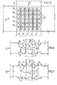
- the electrical connection device of FIG. 5 results from a application of the principle of FIG. 4 symmetrically for each of the tracks 1 and 2.
- track 2 is penetrated by at least one rib of insulating material disposed at a substantially smaller distance from a fitting at a width of the second track at this connection.
- five ribs 7a-7e are arranged in track 2.
- Each rib is parallel to the direction of passage I2 of the electric current in track 2 and crosses the track 2 between its lower and upper faces.
- Connections 3 are then arranged between tracks 1 and 2, so that at least one of the ribs 6a-6e separates any two fittings at their respective interfaces with track 1, and so that at least one of the ribs 7a-7e separates two any connections at their respective interfaces with track 2.
- all of the fittings 3 forms a matrix inserted line by line with the ribs 6a-6e of track 1 in direction I2, and inserted line by line with the ribs 7a-7e of the track 2 in direction I1.
- the edges of track 1 are arranged in the form of slots extending over the entire height of track 1 in the direction D which is perpendicular to the plane of FIG. 6
- These slots include on the one hand faces 9 parallel to the direction I1, which correspond to the interface between the track 1 and the insulating material which surrounds it, present in the configuration shown in FIG. 1 and known from prior art. They also include faces perpendicular to the direction I1, referenced 8 in FIG. 6, inserted between the faces 9.
- the faces 8 constitute additional interface portions.
- Some of the additional interface portions 8 are located at a distance d from the connection 3 less than the width I 1 of the track 1. They have sites for grouping the elementary voids v e additional with respect to the sites present on the faces 9. Consequently, the quantity of elementary voids v e which diffuse in the direction of the interface between the connection 3 and the track 1 is reduced in proportion to the surface of the portions of additional interfaces provided by the slot structure, according to the principle of l 'invention.
- FIG. 7 represents a variant of the configuration of FIG. 6, in which the slots are arranged outside of track 1, with respect to at the width I of track 1 in a portion of track 1 away from connection 3.
- Such a configuration makes it possible to maintain an effective width for the passage of constant current I1 over the entire length of track 1.
- the third mode of implementation of the invention consisting of the provision of slots on some of the faces of track 1 in the electrical connection area of track 1 with track 2, can advantageously be combined with the first and / or the second mode of production.
Landscapes
- Internal Circuitry In Semiconductor Integrated Circuit Devices (AREA)
- Multi-Conductor Connections (AREA)
Applications Claiming Priority (2)
| Application Number | Priority Date | Filing Date | Title |
|---|---|---|---|
| FR0214242 | 2002-11-14 | ||
| FR0214242 | 2002-11-14 |
Publications (2)
| Publication Number | Publication Date |
|---|---|
| EP1420443A2 true EP1420443A2 (de) | 2004-05-19 |
| EP1420443A3 EP1420443A3 (de) | 2014-10-15 |
Family
ID=32116613
Family Applications (1)
| Application Number | Title | Priority Date | Filing Date |
|---|---|---|---|
| EP03292536.4A Withdrawn EP1420443A3 (de) | 2002-11-14 | 2003-10-13 | Elektrische Verbindungsstruktur zwischen zwei Leiterbahnen auf einer integrierten Schaltung |
Country Status (3)
| Country | Link |
|---|---|
| US (1) | US6917116B2 (de) |
| EP (1) | EP1420443A3 (de) |
| JP (1) | JP2004165672A (de) |
Families Citing this family (1)
| Publication number | Priority date | Publication date | Assignee | Title |
|---|---|---|---|---|
| US8435802B2 (en) | 2006-05-22 | 2013-05-07 | Taiwan Semiconductor Manufacturing Co., Ltd. | Conductor layout technique to reduce stress-induced void formations |
Family Cites Families (19)
| Publication number | Priority date | Publication date | Assignee | Title |
|---|---|---|---|---|
| JPH02192146A (ja) * | 1989-01-20 | 1990-07-27 | Toshiba Corp | 半導体装置 |
| EP0393635B1 (de) * | 1989-04-21 | 1997-09-03 | Nec Corporation | Halbleiteranordnung mit Mehrschichtleiter |
| JP2811126B2 (ja) * | 1991-05-02 | 1998-10-15 | 三菱電機株式会社 | 半導体集積回路装置の配線接続構造およびその製造方法 |
| US5434452A (en) * | 1993-11-01 | 1995-07-18 | Motorola, Inc. | Z-axis compliant mechanical IC wiring substrate and method for making the same |
| US5457344A (en) * | 1994-03-25 | 1995-10-10 | Bartelink; Dirk J. | Test fixtures for C4 solder-bump technology |
| JP3432284B2 (ja) * | 1994-07-04 | 2003-08-04 | 三菱電機株式会社 | 半導体装置 |
| US5446311A (en) * | 1994-09-16 | 1995-08-29 | International Business Machines Corporation | High-Q inductors in silicon technology without expensive metalization |
| JPH08293523A (ja) * | 1995-02-21 | 1996-11-05 | Seiko Epson Corp | 半導体装置およびその製造方法 |
| JP3287181B2 (ja) * | 1995-08-15 | 2002-05-27 | ソニー株式会社 | 多層配線の接続構造 |
| US6043562A (en) * | 1996-01-26 | 2000-03-28 | Micron Technology, Inc. | Digit line architecture for dynamic memory |
| US6603646B2 (en) * | 1997-04-08 | 2003-08-05 | X2Y Attenuators, Llc | Multi-functional energy conditioner |
| JP3941156B2 (ja) * | 1997-05-21 | 2007-07-04 | ソニー株式会社 | 半導体装置の製造方法 |
| US5932928A (en) * | 1997-07-03 | 1999-08-03 | Micron Technology, Inc. | Semiconductor circuit interconnections and methods of making such interconnections |
| JP2974022B1 (ja) * | 1998-10-01 | 1999-11-08 | ヤマハ株式会社 | 半導体装置のボンディングパッド構造 |
| US6207553B1 (en) * | 1999-01-26 | 2001-03-27 | Advanced Micro Devices, Inc. | Method of forming multiple levels of patterned metallization |
| US6218282B1 (en) * | 1999-02-18 | 2001-04-17 | Advanced Micro Devices, Inc. | Method of forming low dielectric tungsten lined interconnection system |
| SE518181C2 (sv) * | 1999-12-10 | 2002-09-03 | Ericsson Telefon Ab L M | Förfarande och anordning vid elektroniska kretsarrangemang |
| JP2002208633A (ja) * | 2001-01-10 | 2002-07-26 | Matsushita Electric Ind Co Ltd | 半導体装置およびその製造方法 |
| JP3974470B2 (ja) * | 2002-07-22 | 2007-09-12 | 株式会社東芝 | 半導体装置 |
-
2003
- 2003-10-13 EP EP03292536.4A patent/EP1420443A3/de not_active Withdrawn
- 2003-11-14 US US10/714,442 patent/US6917116B2/en not_active Expired - Lifetime
- 2003-11-14 JP JP2003385102A patent/JP2004165672A/ja active Pending
Non-Patent Citations (1)
| Title |
|---|
| None * |
Also Published As
| Publication number | Publication date |
|---|---|
| US20040140565A1 (en) | 2004-07-22 |
| EP1420443A3 (de) | 2014-10-15 |
| US6917116B2 (en) | 2005-07-12 |
| JP2004165672A (ja) | 2004-06-10 |
Similar Documents
| Publication | Publication Date | Title |
|---|---|---|
| EP0221616B1 (de) | Optoelektronisches Bauelement für Oberflächeneinbau und Herstellungsverfahren | |
| EP0994503A1 (de) | Struktur mit einer dünnen Schicht aus einem aus elektrisch leitfähigen und isolierenden Zonen zusammengesetztem Material und zugehöriges Herstellungsverfahren | |
| EP2250667A1 (de) | Baugruppe mit einem drahtglied und einem mikroelektronischen chip mit einer kerbe mit mindestens einem stift zum halten des drahtglieds | |
| EP1284025A2 (de) | Halbleiter mit vertikaler elektronen-injektion und seine herstellungsmethode | |
| EP1936680A2 (de) | Interconnect-Element auf der Basis von Kohlenstoff-Nanokanälen | |
| WO1999008318A1 (fr) | Procede d'interconnexion a travers un materiau semi-conducteur | |
| FR2803438A1 (fr) | Procede de realisation d'une structure d'interconnexions comprenant une isolation electrique incluant des cavites d'air ou de vide | |
| EP1756872A2 (de) | Mesastruktur-photonerkennungschaltung | |
| EP4222783A1 (de) | Optoelektronische vorrichtung | |
| FR3095719A1 (fr) | Procédé de collage moléculaire hybride et circuit électronique pour la mise en oeuvre d'un tel procédé | |
| EP2263969A2 (de) | Verbessertes Freigabeverfahren der hängenden Struktur eines nanoelektronischen und/oder mikroelektronischen Bauteils | |
| EP2534678B1 (de) | Verbindungsstruktur aus umgeleiteten kohlenstoffnanoröhrchen | |
| EP1420443A2 (de) | Elektrische Verbindungsstruktur zwischen zwei Leiterbahnen auf einer integrierten Schaltung | |
| FR2522203A1 (fr) | Traversee electrique de boitier de circuit hybride et connecteurs complementaires | |
| FR3055166A1 (fr) | Procede de connection intercomposants a densite optimisee | |
| FR2583220A1 (fr) | Procede de realisation d'au moins deux metallisations d'un composant semi-conducteur, recouvertes d'une couche de dielectrique et composant obtenu par ce dielectrique | |
| EP0933812B1 (de) | Elektrochemische Abscheidung von Metallen in Halbleiteranordnungen | |
| EP4006996A2 (de) | Quantenvorrichtung und ihr herstellungsverfahren | |
| EP3832707A1 (de) | Verbindungsstruktur eines phasenwechselspeichers | |
| FR2572852A1 (fr) | Dispositif semi-conducteur en particulier thyristor comportant une electrode d'acces a l'electrode de commande | |
| EP4528806B1 (de) | Elektronischer chip mit anschlusssäulen | |
| FR2789803A1 (fr) | Procede de realisation d'une connexion metallique verticale dans un circuit integre | |
| EP2278613B1 (de) | Röhrenförmige Durchkontaktierung, welche aus mehreren leitfähigen Einzel-Durchkontaktierungen besteht | |
| FR3166783A1 (fr) | Procédé de fabrication d’une structure d’interconnexion électrique haute densité | |
| WO2017203185A1 (fr) | Dispositif a haute mobilite electronique avec elements passifs integres |
Legal Events
| Date | Code | Title | Description |
|---|---|---|---|
| PUAI | Public reference made under article 153(3) epc to a published international application that has entered the european phase |
Free format text: ORIGINAL CODE: 0009012 |
|
| AK | Designated contracting states |
Kind code of ref document: A2 Designated state(s): AT BE BG CH CY CZ DE DK EE ES FI FR GB GR HU IE IT LI LU MC NL PT RO SE SI SK TR |
|
| AX | Request for extension of the european patent |
Extension state: AL LT LV MK |
|
| RAP1 | Party data changed (applicant data changed or rights of an application transferred) |
Owner name: STMICROELECTRONICS S.A. Owner name: NXP B.V. |
|
| RAP1 | Party data changed (applicant data changed or rights of an application transferred) |
Owner name: NXP B.V. |
|
| 17P | Request for examination filed |
Effective date: 20140331 |
|
| PUAL | Search report despatched |
Free format text: ORIGINAL CODE: 0009013 |
|
| AK | Designated contracting states |
Kind code of ref document: A3 Designated state(s): AT BE BG CH CY CZ DE DK EE ES FI FR GB GR HU IE IT LI LU MC NL PT RO SE SI SK TR |
|
| AX | Request for extension of the european patent |
Extension state: AL LT LV MK |
|
| RIC1 | Information provided on ipc code assigned before grant |
Ipc: H01L 21/768 20060101ALI20140910BHEP Ipc: H01L 23/528 20060101ALI20140910BHEP Ipc: H01L 23/522 20060101AFI20140910BHEP |
|
| 17Q | First examination report despatched |
Effective date: 20141120 |
|
| RBV | Designated contracting states (corrected) |
Designated state(s): AT BE BG CH CY CZ DE DK EE ES FI FR GB GR HU IE IT LI LU MC NL PT RO SE SI SK TR |
|
| AKX | Designation fees paid |
Designated state(s): AT BE BG CH CY CZ DE DK EE ES FI FR GB GR HU IE IT LI LU MC NL PT RO SE SI SK TR |
|
| AXX | Extension fees paid |
Extension state: MK Extension state: AL Extension state: LT Extension state: LV |
|
| STAA | Information on the status of an ep patent application or granted ep patent |
Free format text: STATUS: EXAMINATION IS IN PROGRESS |
|
| GRAP | Despatch of communication of intention to grant a patent |
Free format text: ORIGINAL CODE: EPIDOSNIGR1 |
|
| STAA | Information on the status of an ep patent application or granted ep patent |
Free format text: STATUS: GRANT OF PATENT IS INTENDED |
|
| INTG | Intention to grant announced |
Effective date: 20180614 |
|
| STAA | Information on the status of an ep patent application or granted ep patent |
Free format text: STATUS: THE APPLICATION IS DEEMED TO BE WITHDRAWN |
|
| 18D | Application deemed to be withdrawn |
Effective date: 20181025 |