EP1409237B1 - Verfahren zur sanften programmierung eines dual-zellen-speichers mit virtueller masse - Google Patents
Verfahren zur sanften programmierung eines dual-zellen-speichers mit virtueller masse Download PDFInfo
- Publication number
- EP1409237B1 EP1409237B1 EP02739278A EP02739278A EP1409237B1 EP 1409237 B1 EP1409237 B1 EP 1409237B1 EP 02739278 A EP02739278 A EP 02739278A EP 02739278 A EP02739278 A EP 02739278A EP 1409237 B1 EP1409237 B1 EP 1409237B1
- Authority
- EP
- European Patent Office
- Prior art keywords
- cells
- soft
- source
- pair
- programming
- Prior art date
- Legal status (The legal status is an assumption and is not a legal conclusion. Google has not performed a legal analysis and makes no representation as to the accuracy of the status listed.)
- Expired - Lifetime
Links
- 230000015654 memory Effects 0.000 title claims abstract description 62
- 238000003491 array Methods 0.000 title abstract description 7
- 238000000034 method Methods 0.000 claims abstract description 48
- 238000002347 injection Methods 0.000 claims abstract description 11
- 239000007924 injection Substances 0.000 claims abstract description 11
- 230000009977 dual effect Effects 0.000 abstract description 5
- 210000004027 cell Anatomy 0.000 description 161
- 230000008569 process Effects 0.000 description 24
- 230000000694 effects Effects 0.000 description 5
- 238000012795 verification Methods 0.000 description 4
- 238000013459 approach Methods 0.000 description 3
- 238000010586 diagram Methods 0.000 description 3
- 230000005283 ground state Effects 0.000 description 3
- 230000008878 coupling Effects 0.000 description 2
- 238000010168 coupling process Methods 0.000 description 2
- 238000005859 coupling reaction Methods 0.000 description 2
- 238000009826 distribution Methods 0.000 description 2
- 238000004519 manufacturing process Methods 0.000 description 2
- 230000007246 mechanism Effects 0.000 description 2
- 230000008439 repair process Effects 0.000 description 2
- 101150107986 CGR2 gene Proteins 0.000 description 1
- 210000000227 basophil cell of anterior lobe of hypophysis Anatomy 0.000 description 1
- 238000013329 compounding Methods 0.000 description 1
- 239000004020 conductor Substances 0.000 description 1
- 230000001419 dependent effect Effects 0.000 description 1
- 238000011161 development Methods 0.000 description 1
- 238000009792 diffusion process Methods 0.000 description 1
- 230000005684 electric field Effects 0.000 description 1
- 239000002184 metal Substances 0.000 description 1
- 230000008450 motivation Effects 0.000 description 1
- 230000002093 peripheral effect Effects 0.000 description 1
- 230000004044 response Effects 0.000 description 1
- 239000000243 solution Substances 0.000 description 1
- 238000003860 storage Methods 0.000 description 1
- 238000012546 transfer Methods 0.000 description 1
Images






Classifications
-
- G—PHYSICS
- G11—INFORMATION STORAGE
- G11C—STATIC STORES
- G11C16/00—Erasable programmable read-only memories
- G11C16/02—Erasable programmable read-only memories electrically programmable
- G11C16/06—Auxiliary circuits, e.g. for writing into memory
- G11C16/10—Programming or data input circuits
- G11C16/14—Circuits for erasing electrically, e.g. erase voltage switching circuits
-
- G—PHYSICS
- G11—INFORMATION STORAGE
- G11C—STATIC STORES
- G11C16/00—Erasable programmable read-only memories
- G11C16/02—Erasable programmable read-only memories electrically programmable
- G11C16/06—Auxiliary circuits, e.g. for writing into memory
- G11C16/34—Determination of programming status, e.g. threshold voltage, overprogramming or underprogramming, retention
- G11C16/3404—Convergence or correction of memory cell threshold voltages; Repair or recovery of overerased or overprogrammed cells
-
- G—PHYSICS
- G11—INFORMATION STORAGE
- G11C—STATIC STORES
- G11C16/00—Erasable programmable read-only memories
- G11C16/02—Erasable programmable read-only memories electrically programmable
- G11C16/04—Erasable programmable read-only memories electrically programmable using variable threshold transistors, e.g. FAMOS
- G11C16/0491—Virtual ground arrays
-
- G—PHYSICS
- G11—INFORMATION STORAGE
- G11C—STATIC STORES
- G11C16/00—Erasable programmable read-only memories
- G11C16/02—Erasable programmable read-only memories electrically programmable
- G11C16/06—Auxiliary circuits, e.g. for writing into memory
- G11C16/10—Programming or data input circuits
- G11C16/12—Programming voltage switching circuits
-
- G—PHYSICS
- G11—INFORMATION STORAGE
- G11C—STATIC STORES
- G11C16/00—Erasable programmable read-only memories
- G11C16/02—Erasable programmable read-only memories electrically programmable
- G11C16/06—Auxiliary circuits, e.g. for writing into memory
- G11C16/24—Bit-line control circuits
Definitions
- the drain is usually set in a range of 4 to 7 volts, say 5 volts and the source is set to ground below the current limiter 531.
- the actual voltage on the source of the transistor depends on the cell characteristics that vary across the array. All of the cells in a column will be biased the same way.
- the word-lines of the selected cells are then pulsed with the programming voltage, usually in the range of 5-10 volts when data is being stored on the cell.
- the side-wall is capacitively coupled to the control gate and the programming voltage causes the electrons flowing through the channel to be injected into the floating gate.
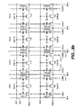
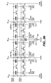
- ⁇ 2 forms a pair with ⁇ 5 and is soft programmed when bit-line 913 is taken as the source and bit-lines 912 and 914 are drains, as shown in Figure 9b .
- bit-line 913 is taken as the source
- bit-lines 912 and 914 are drains, as shown in Figure 9b .
- the ⁇ 1 - ⁇ 3 pair, the ⁇ 1 - ⁇ 3 pair, and any others not on the figure can also be soft-programmed.
- these floating gates can be soft programmed until either all of the pairs in these groups verify, or until a first pair in these groups verifies. The latter case is similar to how the pair verification is performed, with the programming of other gates in the columns determined by the verification of the first pair to reach the desired state.
- cells from different groups will vary more than adjoining cells, they will still also have similar electrical characteristics and should therefore program at a similar rate. If instead every pair in the different groups is independently verified, a tighter distribution will be realized, but at the expense of time.
Landscapes
- Engineering & Computer Science (AREA)
- Microelectronics & Electronic Packaging (AREA)
- Read Only Memory (AREA)
- Non-Volatile Memory (AREA)
- Semiconductor Memories (AREA)
- Techniques For Improving Reliability Of Storages (AREA)
Claims (10)
- Verfahren zum Behandeln von gelöschten Speicherzellen in einem nichtflüchtigen Speicher (500) mit einer Vielzahl von Speicherzellen (α, β), die eine virtuelle Masse-Anordnung bilden, bestehend aus einer oder mehr Reihen (WL) davon, wobei jede Speicherzelle erste und zweite Source-/Drain-Regionen aufweist, die mit Bitleitungen (BL) verbunden sind, die senkrecht zu den Reihen von Zellen sind, in denen eine sanfte Programmieroperation (6, 7) gleichzeitig an einem Paar von Speicherzellen (533) ausgeführt wird, bestehend aus einer ersten Speicherzelle, die zu einem anderen Zustand als einem von mindestens zwei Datenzuständen gelöscht wurde, und einer zweiten Speicherzelle, mit der die Speicherzelle, die zu einem anderen Zustand als einem von mindestens zwei Datenzuständen gelöscht wurde, eine Bitleitung gemeinsam nutzt, mit der beide Zellen ihre jeweilige Source-/Drain-Region verbunden haben,
dadurch gekennzeichnet, dass
der Zustand einer besagten ersten Speicherzelle vor der sanften Programmieroperation erfasst wird (603) und dieses Paar von Zellen nur dann sanft programmiert wird, wenn beide Zellen zu einem anderen Zustand als einem von mindestens zwei Datenzuständen gelöscht wurde,
und durch
Erfassen (609) im Anschluss an die sanfte Programmieroperation, ob das Paar von Speicherzellen zu einem anderen Zustand als einem von mindestens zwei Datenzuständen gelöscht bleibt, und als Reaktion darauf, abwechselndes Wiederholen (611) der sanften Programmieroperation und des Erfassens so lange, wie beide Speicherzellen des Paars zu einem anderen Zustand als einem von mindestens zwei Datenzuständen gelöscht bleiben. - Verfahren nach Anspruch 1, wobei die sanfte Programmieroperation (607) umfasst, eine sanfte Programmspannung anzulegen, die niedriger als eine Standard-Programmierspannung ist.
- Verfahren nach Anspruch 2, wobei die sanfte Programmieroperation (607) unter Verwendung einer Spannung im Bereich von 4 bis 7 Volt für die erste Source-/Drain-Region des Paars von Speicherzellen ausgeführt wird.
- Verfahren nach einem der vorstehenden Ansprüche, wobei die Speicherzellen elektrisch löschbare und programmierbare Nur-Lese-Speicherzellen (EEPROM) mit Source-seitiger Injektion sind und wobei die zweite Source-/Drain-Region eine Source ist.
- Verfahren nach Anspruch 4, wobei die sanfte Programmieroperation (607) durch Source-seitige Injektion erfolgt.
- Verfahren nach einem der vorstehenden Ansprüche, wobei die Speicherzellen elektrisch löschbare und programmierbare Nur-Lese-Speicherzellen (EEPROM) sind und jede der Speicherzellen (α, β) weiterhin eine Kanalregion mit einem ersten und einem zweiten Abschnitt umfasst, die zwischen den und jeweils angrenzend an den ersten und zweiten Source-/Drain-Regionen liegen, einen ersten Schwebegate über dem ersten Abschnitt der Kanalregion, einen ersten Steuergate mit einem Abschnitt über dem ersten Schwebegate, einen zweiten Schwebegate über dem zweiten Abschnitt der Kanalregion und einen zweiten Steuergate mit einem Abschnitt über dem zweiten Schwebegate, und wobei jede der Speicherzellen weiterhin eine dritte Kanalregion umfasst, die zwischen den ersten und zweiten Kanalregionen liegt, und ein Auswahlgate mit einem Abschnitt über dem dritten Abschnitt der Kanalregion.
- Verfahren nach Anspruch 6, wobei die sanfte Programmieroperation an dem ersten Schwebegate von jeder des Paars von Speicherzellen ausgeführt wird.
- Verfahren nach Anspruch 7, wobei die sanfte Programmieroperation enthält, eine Spannung an den zweiten Steuergate von jeder des Paars von Speicherzellen anzulegen, die ausreichend ist, um zuzulassen, dass Strom frei durch den zweiten Abschnitt der Kanalregion fließt, wodurch sanfte Programmierung an nur dem ersten Schwebegate von jeder des Paars von Speicherzellen ausgeführt wird.
- Verfahren nach Anspruch 8, wobei die sanfte Programmierung unter Verwendung einer Spannung im Bereich von vier Volt bis sieben Volt für die erste Source-/Drain-Region ausgeführt wird und die Spannung zu dem zweiten Steuergate, die ausreichend ist, um zuzulassen, dass Strom frei durch den zweiten Abschnitt der Kanalregion fließt, eine Spannung im Bereich von acht Volt bis zwölf Volt ist.
- Verfahren nach einem der Ansprüche 6 bis 9, wobei die gleichzeitige sanfte Programmieroperation ausgeführt wird, indem eine Spannung im Bereich von 1,5 Volt bis 3 Volt an den zweiten Auswahlgate von dem Paar von Speicherzellen angelegt wird.
Applications Claiming Priority (3)
| Application Number | Priority Date | Filing Date | Title |
|---|---|---|---|
| US09/865,320 US6522585B2 (en) | 2001-05-25 | 2001-05-25 | Dual-cell soft programming for virtual-ground memory arrays |
| US865320 | 2001-05-25 | ||
| PCT/US2002/015570 WO2002096632A2 (en) | 2001-05-25 | 2002-05-17 | Dual-cell soft programming for virtual-ground memory arrays |
Publications (2)
| Publication Number | Publication Date |
|---|---|
| EP1409237A2 EP1409237A2 (de) | 2004-04-21 |
| EP1409237B1 true EP1409237B1 (de) | 2008-10-29 |
Family
ID=25345234
Family Applications (1)
| Application Number | Title | Priority Date | Filing Date |
|---|---|---|---|
| EP02739278A Expired - Lifetime EP1409237B1 (de) | 2001-05-25 | 2002-05-17 | Verfahren zur sanften programmierung eines dual-zellen-speichers mit virtueller masse |
Country Status (9)
| Country | Link |
|---|---|
| US (1) | US6522585B2 (de) |
| EP (1) | EP1409237B1 (de) |
| JP (1) | JP4212901B2 (de) |
| KR (1) | KR100897590B1 (de) |
| AT (1) | ATE412964T1 (de) |
| AU (1) | AU2002311936A1 (de) |
| DE (1) | DE60229641D1 (de) |
| TW (1) | TW559816B (de) |
| WO (1) | WO2002096632A2 (de) |
Families Citing this family (99)
| Publication number | Priority date | Publication date | Assignee | Title |
|---|---|---|---|---|
| US6768165B1 (en) * | 1997-08-01 | 2004-07-27 | Saifun Semiconductors Ltd. | Two bit non-volatile electrically erasable and programmable semiconductor memory cell utilizing asymmetrical charge trapping |
| US6928001B2 (en) | 2000-12-07 | 2005-08-09 | Saifun Semiconductors Ltd. | Programming and erasing methods for a non-volatile memory cell |
| US6584017B2 (en) | 2001-04-05 | 2003-06-24 | Saifun Semiconductors Ltd. | Method for programming a reference cell |
| US7098107B2 (en) * | 2001-11-19 | 2006-08-29 | Saifun Semiconductor Ltd. | Protective layer in memory device and method therefor |
| US20030141537A1 (en) * | 2001-12-28 | 2003-07-31 | Xiaoju Wu | System for multiple input floating gate structures |
| US7190620B2 (en) * | 2002-01-31 | 2007-03-13 | Saifun Semiconductors Ltd. | Method for operating a memory device |
| US6700818B2 (en) * | 2002-01-31 | 2004-03-02 | Saifun Semiconductors Ltd. | Method for operating a memory device |
| US6975536B2 (en) * | 2002-01-31 | 2005-12-13 | Saifun Semiconductors Ltd. | Mass storage array and methods for operation thereof |
| TWI259952B (en) * | 2002-01-31 | 2006-08-11 | Macronix Int Co Ltd | Data erase method of flash memory |
| US6795349B2 (en) * | 2002-02-28 | 2004-09-21 | Sandisk Corporation | Method and system for efficiently reading and programming of dual cell memory elements |
| US6917544B2 (en) | 2002-07-10 | 2005-07-12 | Saifun Semiconductors Ltd. | Multiple use memory chip |
| US7136304B2 (en) | 2002-10-29 | 2006-11-14 | Saifun Semiconductor Ltd | Method, system and circuit for programming a non-volatile memory array |
| US6963505B2 (en) | 2002-10-29 | 2005-11-08 | Aifun Semiconductors Ltd. | Method circuit and system for determining a reference voltage |
| US6992932B2 (en) | 2002-10-29 | 2006-01-31 | Saifun Semiconductors Ltd | Method circuit and system for read error detection in a non-volatile memory array |
| US6967896B2 (en) * | 2003-01-30 | 2005-11-22 | Saifun Semiconductors Ltd | Address scramble |
| US7178004B2 (en) * | 2003-01-31 | 2007-02-13 | Yan Polansky | Memory array programming circuit and a method for using the circuit |
| ITTO20030115A1 (it) * | 2003-02-17 | 2004-08-18 | St Microelectronics Srl | Metodo di soft-programmazione per un dispositivo di |
| US6768673B1 (en) * | 2003-04-24 | 2004-07-27 | Advanced Micro Devices, Inc. | Method of programming and reading a dual cell memory device |
| US7142464B2 (en) * | 2003-04-29 | 2006-11-28 | Saifun Semiconductors Ltd. | Apparatus and methods for multi-level sensing in a memory array |
| US7085170B2 (en) * | 2003-08-07 | 2006-08-01 | Micron Technology, Ind. | Method for erasing an NROM cell |
| US7123532B2 (en) * | 2003-09-16 | 2006-10-17 | Saifun Semiconductors Ltd. | Operating array cells with matched reference cells |
| US7652930B2 (en) * | 2004-04-01 | 2010-01-26 | Saifun Semiconductors Ltd. | Method, circuit and system for erasing one or more non-volatile memory cells |
| US7009887B1 (en) * | 2004-06-03 | 2006-03-07 | Fasl Llc | Method of determining voltage compensation for flash memory devices |
| US7366025B2 (en) * | 2004-06-10 | 2008-04-29 | Saifun Semiconductors Ltd. | Reduced power programming of non-volatile cells |
| US7307884B2 (en) * | 2004-06-15 | 2007-12-11 | Sandisk Corporation | Concurrent programming of non-volatile memory |
| US7120059B2 (en) * | 2004-07-06 | 2006-10-10 | Macronix International Co., Ltd. | Memory array including multiple-gate charge trapping non-volatile cells |
| US7106625B2 (en) * | 2004-07-06 | 2006-09-12 | Macronix International Co, Td | Charge trapping non-volatile memory with two trapping locations per gate, and method for operating same |
| US7209386B2 (en) * | 2004-07-06 | 2007-04-24 | Macronix International Co., Ltd. | Charge trapping non-volatile memory and method for gate-by-gate erase for same |
| US20060007732A1 (en) * | 2004-07-06 | 2006-01-12 | Macronix International Co., Ltd. | Charge trapping non-volatile memory and method for operating same |
| US7387932B2 (en) * | 2004-07-06 | 2008-06-17 | Macronix International Co., Ltd. | Method for manufacturing a multiple-gate charge trapping non-volatile memory |
| US6987696B1 (en) * | 2004-07-06 | 2006-01-17 | Advanced Micro Devices, Inc. | Method of improving erase voltage distribution for a flash memory array having dummy wordlines |
| US7317633B2 (en) | 2004-07-06 | 2008-01-08 | Saifun Semiconductors Ltd | Protection of NROM devices from charge damage |
| US7042766B1 (en) | 2004-07-22 | 2006-05-09 | Spansion, Llc | Method of programming a flash memory device using multilevel charge storage |
| US7042767B2 (en) * | 2004-08-02 | 2006-05-09 | Spansion, Llc | Flash memory unit and method of programming a flash memory device |
| US7095655B2 (en) * | 2004-08-12 | 2006-08-22 | Saifun Semiconductors Ltd. | Dynamic matching of signal path and reference path for sensing |
| US20060068551A1 (en) * | 2004-09-27 | 2006-03-30 | Saifun Semiconductors, Ltd. | Method for embedding NROM |
| US7638850B2 (en) * | 2004-10-14 | 2009-12-29 | Saifun Semiconductors Ltd. | Non-volatile memory structure and method of fabrication |
| US20060146624A1 (en) * | 2004-12-02 | 2006-07-06 | Saifun Semiconductors, Ltd. | Current folding sense amplifier |
| US7242618B2 (en) * | 2004-12-09 | 2007-07-10 | Saifun Semiconductors Ltd. | Method for reading non-volatile memory cells |
| US7535765B2 (en) | 2004-12-09 | 2009-05-19 | Saifun Semiconductors Ltd. | Non-volatile memory device and method for reading cells |
| US7230851B2 (en) * | 2004-12-23 | 2007-06-12 | Sandisk Corporation | Reducing floating gate to floating gate coupling effect |
| US7315474B2 (en) | 2005-01-03 | 2008-01-01 | Macronix International Co., Ltd | Non-volatile memory cells, memory arrays including the same and methods of operating cells and arrays |
| US7473589B2 (en) * | 2005-12-09 | 2009-01-06 | Macronix International Co., Ltd. | Stacked thin film transistor, non-volatile memory devices and methods for fabricating the same |
| US8482052B2 (en) | 2005-01-03 | 2013-07-09 | Macronix International Co., Ltd. | Silicon on insulator and thin film transistor bandgap engineered split gate memory |
| EP1684308A1 (de) | 2005-01-19 | 2006-07-26 | Saifun Semiconductors Ltd. | Verfahren zur Verhinderung von Feststrukturprogrammierung |
| TWI254458B (en) * | 2005-03-04 | 2006-05-01 | Powerchip Semiconductor Corp | Non-volatile memory and manufacturing method and operating method thereof |
| US8053812B2 (en) | 2005-03-17 | 2011-11-08 | Spansion Israel Ltd | Contact in planar NROM technology |
| US7158420B2 (en) | 2005-04-29 | 2007-01-02 | Macronix International Co., Ltd. | Inversion bit line, charge trapping non-volatile memory and method of operating same |
| US20070141788A1 (en) * | 2005-05-25 | 2007-06-21 | Ilan Bloom | Method for embedding non-volatile memory with logic circuitry |
| US8400841B2 (en) * | 2005-06-15 | 2013-03-19 | Spansion Israel Ltd. | Device to program adjacent storage cells of different NROM cells |
| US7184313B2 (en) * | 2005-06-17 | 2007-02-27 | Saifun Semiconductors Ltd. | Method circuit and system for compensating for temperature induced margin loss in non-volatile memory cells |
| US7355903B2 (en) * | 2005-07-15 | 2008-04-08 | Macronix International Co., Ltd. | Semiconductor device including memory cells and current limiter |
| JP2007027760A (ja) * | 2005-07-18 | 2007-02-01 | Saifun Semiconductors Ltd | 高密度不揮発性メモリアレイ及び製造方法 |
| US20070030736A1 (en) * | 2005-08-03 | 2007-02-08 | Fabiano Fontana | Variable source resistor for flash memory |
| US7763927B2 (en) * | 2005-12-15 | 2010-07-27 | Macronix International Co., Ltd. | Non-volatile memory device having a nitride-oxide dielectric layer |
| US20070036007A1 (en) * | 2005-08-09 | 2007-02-15 | Saifun Semiconductors, Ltd. | Sticky bit buffer |
| US7668017B2 (en) | 2005-08-17 | 2010-02-23 | Saifun Semiconductors Ltd. | Method of erasing non-volatile memory cells |
| US8116142B2 (en) * | 2005-09-06 | 2012-02-14 | Infineon Technologies Ag | Method and circuit for erasing a non-volatile memory cell |
| US20070096199A1 (en) * | 2005-09-08 | 2007-05-03 | Eli Lusky | Method of manufacturing symmetric arrays |
| US7221138B2 (en) | 2005-09-27 | 2007-05-22 | Saifun Semiconductors Ltd | Method and apparatus for measuring charge pump output current |
| US7218563B1 (en) * | 2005-11-18 | 2007-05-15 | Macronix International Co., Ltd. | Method and apparatus for reading data from nonvolatile memory |
| US20070120180A1 (en) * | 2005-11-25 | 2007-05-31 | Boaz Eitan | Transition areas for dense memory arrays |
| US7352627B2 (en) * | 2006-01-03 | 2008-04-01 | Saifon Semiconductors Ltd. | Method, system, and circuit for operating a non-volatile memory array |
| US7808818B2 (en) * | 2006-01-12 | 2010-10-05 | Saifun Semiconductors Ltd. | Secondary injection for NROM |
| US20070173017A1 (en) * | 2006-01-20 | 2007-07-26 | Saifun Semiconductors, Ltd. | Advanced non-volatile memory array and method of fabrication thereof |
| US7760554B2 (en) * | 2006-02-21 | 2010-07-20 | Saifun Semiconductors Ltd. | NROM non-volatile memory and mode of operation |
| US8253452B2 (en) * | 2006-02-21 | 2012-08-28 | Spansion Israel Ltd | Circuit and method for powering up an integrated circuit and an integrated circuit utilizing same |
| US7692961B2 (en) * | 2006-02-21 | 2010-04-06 | Saifun Semiconductors Ltd. | Method, circuit and device for disturb-control of programming nonvolatile memory cells by hot-hole injection (HHI) and by channel hot-electron (CHE) injection |
| US7638835B2 (en) | 2006-02-28 | 2009-12-29 | Saifun Semiconductors Ltd. | Double density NROM with nitride strips (DDNS) |
| US20070255889A1 (en) * | 2006-03-22 | 2007-11-01 | Yoav Yogev | Non-volatile memory device and method of operating the device |
| US7701779B2 (en) * | 2006-04-27 | 2010-04-20 | Sajfun Semiconductors Ltd. | Method for programming a reference cell |
| US7907450B2 (en) * | 2006-05-08 | 2011-03-15 | Macronix International Co., Ltd. | Methods and apparatus for implementing bit-by-bit erase of a flash memory device |
| FR2901626A1 (fr) * | 2006-05-29 | 2007-11-30 | St Microelectronics Sa | Memoire eeprom ayant une resistance contre le claquage de transistors amelioree |
| US7605579B2 (en) * | 2006-09-18 | 2009-10-20 | Saifun Semiconductors Ltd. | Measuring and controlling current consumption and output current of charge pumps |
| KR100879387B1 (ko) * | 2006-09-22 | 2009-01-20 | 삼성전자주식회사 | 플래시 메모리 장치 및 그것의 프로그램 방법 |
| US8772858B2 (en) * | 2006-10-11 | 2014-07-08 | Macronix International Co., Ltd. | Vertical channel memory and manufacturing method thereof and operating method using the same |
| US7811890B2 (en) * | 2006-10-11 | 2010-10-12 | Macronix International Co., Ltd. | Vertical channel transistor structure and manufacturing method thereof |
| US7499317B2 (en) * | 2006-10-13 | 2009-03-03 | Sandisk Corporation | System for partitioned erase and erase verification in a non-volatile memory to compensate for capacitive coupling |
| US7495954B2 (en) * | 2006-10-13 | 2009-02-24 | Sandisk Corporation | Method for partitioned erase and erase verification to compensate for capacitive coupling effects in non-volatile memory |
| US7499338B2 (en) * | 2006-10-13 | 2009-03-03 | Sandisk Corporation | Partitioned soft programming in non-volatile memory |
| US7535766B2 (en) * | 2006-10-13 | 2009-05-19 | Sandisk Corporation | Systems for partitioned soft programming in non-volatile memory |
| US7944749B2 (en) | 2006-12-21 | 2011-05-17 | Sandisk Corporation | Method of low voltage programming of non-volatile memory cells |
| US7623389B2 (en) | 2006-12-21 | 2009-11-24 | Sandisk Corporation | System for low voltage programming of non-volatile memory cells |
| EP2102868B1 (de) * | 2006-12-21 | 2016-02-24 | SanDisk Technologies Inc. | Verfahren und system zur niedrigspannungsprogrammierung nicht-flüchtiger speicherzellen |
| US7385851B1 (en) * | 2006-12-22 | 2008-06-10 | Spansion Llc | Repetitive erase verify technique for flash memory devices |
| US7564715B2 (en) * | 2007-02-20 | 2009-07-21 | Sandisk Corporation | Variable initial program voltage magnitude for non-volatile storage |
| US20080239599A1 (en) * | 2007-04-01 | 2008-10-02 | Yehuda Yizraeli | Clamping Voltage Events Such As ESD |
| US7668018B2 (en) * | 2007-04-03 | 2010-02-23 | Freescale Semiconductor, Inc. | Electronic device including a nonvolatile memory array and methods of using the same |
| US20080285368A1 (en) * | 2007-05-17 | 2008-11-20 | Macronix International Co., Ltd. | Method for nrom array word line retry erasing and threshold voltage recovering |
| US20090039414A1 (en) * | 2007-08-09 | 2009-02-12 | Macronix International Co., Ltd. | Charge trapping memory cell with high speed erase |
| US7707371B1 (en) | 2007-09-10 | 2010-04-27 | Cisco Technology, Inc. | Storage area network (SAN) switch multi-pass erase of data on target devices |
| JP5754761B2 (ja) * | 2008-07-22 | 2015-07-29 | ラピスセミコンダクタ株式会社 | 不揮発性半導体メモリおよび不揮発性半導体メモリのデータ書込み方法 |
| DE102008041891A1 (de) * | 2008-09-09 | 2010-03-18 | Qimonda Ag | Integrierte Halbleiterschaltung mit einer Bitleitung zum Ansteuern zweiter Reihen aktiver Gebiete und Herstellungsverfahren für eine derartige integrierte Halbleiterschaltung |
| KR101497548B1 (ko) * | 2009-02-02 | 2015-03-03 | 삼성전자주식회사 | 플래시 메모리 장치, 및 이의 프로그램 및 독출 방법 |
| CN101807433B (zh) * | 2010-03-10 | 2012-10-24 | 上海宏力半导体制造有限公司 | 一种存储器的编程方法 |
| US9240405B2 (en) | 2011-04-19 | 2016-01-19 | Macronix International Co., Ltd. | Memory with off-chip controller |
| CN102568558B (zh) * | 2012-02-28 | 2017-12-08 | 上海华虹宏力半导体制造有限公司 | 存储器的操作方法 |
| US9953719B2 (en) * | 2016-05-18 | 2018-04-24 | Silicon Storage Technology, Inc. | Flash memory cell and associated decoders |
| TWI678700B (zh) * | 2019-03-07 | 2019-12-01 | 億而得微電子股份有限公司 | 低電流電子抹除式可複寫唯讀記憶體陣列的快速抹除方法 |
Family Cites Families (19)
| Publication number | Priority date | Publication date | Assignee | Title |
|---|---|---|---|---|
| JPS5955071A (ja) | 1982-09-24 | 1984-03-29 | Hitachi Micro Comput Eng Ltd | 不揮発性半導体装置 |
| US5172338B1 (en) | 1989-04-13 | 1997-07-08 | Sandisk Corp | Multi-state eeprom read and write circuits and techniques |
| DE69013237T2 (de) * | 1989-06-19 | 1995-02-23 | Texas Instruments Inc | Schaltung und Verfahren zur Vorbereitung gelöschter EEPROMS vor der Programmierung. |
| JPH04222994A (ja) | 1990-12-26 | 1992-08-12 | Mitsubishi Electric Corp | 不揮発性半導体記憶装置 |
| US5272669A (en) | 1991-02-20 | 1993-12-21 | Sundisk Corporation | Method and structure for programming floating gate memory cells |
| US5267194A (en) | 1991-08-30 | 1993-11-30 | Winbond Electronics Corporation | Electrically erasable programmable read-only-memory cell with side-wall floating gate |
| US5712180A (en) | 1992-01-14 | 1998-01-27 | Sundisk Corporation | EEPROM with split gate source side injection |
| US5619454A (en) | 1993-11-15 | 1997-04-08 | Micron Technology, Inc. | Programming method for healing over-erased cells for a flash memory device |
| US5745410A (en) * | 1995-11-17 | 1998-04-28 | Macronix International Co., Ltd. | Method and system for soft programming algorithm |
| US5673224A (en) * | 1996-02-23 | 1997-09-30 | Micron Quantum Devices, Inc. | Segmented non-volatile memory array with multiple sources with improved word line control circuitry |
| US5768192A (en) | 1996-07-23 | 1998-06-16 | Saifun Semiconductors, Ltd. | Non-volatile semiconductor memory cell utilizing asymmetrical charge trapping |
| KR100323554B1 (ko) * | 1997-05-14 | 2002-03-08 | 니시무로 타이죠 | 불휘발성반도체메모리장치 |
| US5909392A (en) | 1997-10-09 | 1999-06-01 | Programmable Microelectronics Corporation | PMOS memory array having OR gate architecture |
| US5930174A (en) | 1997-12-11 | 1999-07-27 | Amic Technology, Inc. | Circuit and method for erasing flash memory array |
| US5963465A (en) | 1997-12-12 | 1999-10-05 | Saifun Semiconductors, Ltd. | Symmetric segmented memory array architecture |
| US6005807A (en) | 1998-09-16 | 1999-12-21 | Winbond Electronics Corp. | Method and apparatus for self-aligned memory cells and array using source side injection |
| US6128226A (en) | 1999-02-04 | 2000-10-03 | Saifun Semiconductors Ltd. | Method and apparatus for operating with a close to ground signal |
| US6134156A (en) | 1999-02-04 | 2000-10-17 | Saifun Semiconductors Ltd. | Method for initiating a retrieval procedure in virtual ground arrays |
| US6103573A (en) | 1999-06-30 | 2000-08-15 | Sandisk Corporation | Processing techniques for making a dual floating gate EEPROM cell array |
-
2001
- 2001-05-25 US US09/865,320 patent/US6522585B2/en not_active Expired - Fee Related
-
2002
- 2002-05-17 JP JP2002593131A patent/JP4212901B2/ja not_active Expired - Fee Related
- 2002-05-17 AT AT02739278T patent/ATE412964T1/de not_active IP Right Cessation
- 2002-05-17 DE DE60229641T patent/DE60229641D1/de not_active Expired - Lifetime
- 2002-05-17 KR KR1020037001135A patent/KR100897590B1/ko not_active Expired - Fee Related
- 2002-05-17 AU AU2002311936A patent/AU2002311936A1/en not_active Abandoned
- 2002-05-17 EP EP02739278A patent/EP1409237B1/de not_active Expired - Lifetime
- 2002-05-17 WO PCT/US2002/015570 patent/WO2002096632A2/en not_active Ceased
- 2002-05-21 TW TW091110666A patent/TW559816B/zh not_active IP Right Cessation
Also Published As
| Publication number | Publication date |
|---|---|
| KR100897590B1 (ko) | 2009-05-14 |
| TW559816B (en) | 2003-11-01 |
| US20020176280A1 (en) | 2002-11-28 |
| WO2002096632A3 (en) | 2004-02-05 |
| JP2004527868A (ja) | 2004-09-09 |
| ATE412964T1 (de) | 2008-11-15 |
| JP4212901B2 (ja) | 2009-01-21 |
| WO2002096632A2 (en) | 2002-12-05 |
| KR20030043918A (ko) | 2003-06-02 |
| US6522585B2 (en) | 2003-02-18 |
| DE60229641D1 (de) | 2008-12-11 |
| AU2002311936A1 (en) | 2002-12-09 |
| EP1409237A2 (de) | 2004-04-21 |
Similar Documents
| Publication | Publication Date | Title |
|---|---|---|
| US6522585B2 (en) | Dual-cell soft programming for virtual-ground memory arrays | |
| KR102606826B1 (ko) | 비휘발성 메모리 장치 및 그 소거 방법 | |
| US7518908B2 (en) | EEPROM array and method for operation thereof | |
| US10157680B2 (en) | Sub-block mode for non-volatile memory | |
| US6636440B2 (en) | Method for operation of an EEPROM array, including refresh thereof | |
| KR100960352B1 (ko) | 선 소거 단계를 이용하여 플래시 메모리를 소거하는 방법 | |
| US7263000B2 (en) | NAND type memory with dummy cells adjacent to select transistors being biased at different voltage during data erase | |
| US6031765A (en) | Reversed split-gate cell array | |
| US5790456A (en) | Multiple bits-per-cell flash EEPROM memory cells with wide program and erase Vt window | |
| EP0755559B1 (de) | Speichermatrix mit mehrzustandsspeicherzellen | |
| US8879331B2 (en) | Shared bit line string architecture | |
| KR20050003365A (ko) | 두 개의 상보적으로 프로그래밍된 듀얼 비트 기준 셀의전압 평균화에 기초한 기준 전압 생성 시스템 및 방법 | |
| KR20030048159A (ko) | 이중 비트 메모리의 소거 검증 방법 및 시스템 | |
| US20110116311A1 (en) | Reduction of punch-through disturb during programming of a memory device | |
| US5424991A (en) | Floating gate nonvolatile memory with uniformly erased threshold voltage | |
| JP4698605B2 (ja) | 半導体装置および半導体装置の制御方法 | |
| EP1513160B1 (de) | Nichtflüchtiger Flash-Speicher | |
| US6285588B1 (en) | Erase scheme to tighten the threshold voltage distribution of EEPROM flash memory cells | |
| US7286398B2 (en) | Semiconductor device and method of controlling said semiconductor device | |
| KR100888616B1 (ko) | 소거 동작 전에 프리 프로그램 동작을 수행하는 낸드플래시 메모리 및 그것의 소거 방법 | |
| KR101014968B1 (ko) | 불휘발성 메모리 소자와 그 페이지 버퍼 회로 | |
| JP4177167B2 (ja) | 不揮発性半導体記憶装置及びデータ判定方法 | |
| JP2011028845A (ja) | 半導体装置および半導体装置の制御方法 | |
| KR20070086721A (ko) | 반도체 장치 및 반도체 장치의 제어 방법 |
Legal Events
| Date | Code | Title | Description |
|---|---|---|---|
| PUAI | Public reference made under article 153(3) epc to a published international application that has entered the european phase |
Free format text: ORIGINAL CODE: 0009012 |
|
| AK | Designated contracting states |
Kind code of ref document: A2 Designated state(s): AT BE CH CY DE DK ES FI FR GB GR IE IT LI LU MC NL PT SE TR |
|
| AX | Request for extension of the european patent |
Extension state: AL LT LV MK RO SI |
|
| 17P | Request for examination filed |
Effective date: 20040728 |
|
| RIC1 | Information provided on ipc code assigned before grant |
Ipc: G11C 16/34 20060101AFI20060403BHEP Ipc: G11C 16/04 20060101ALI20060403BHEP |
|
| RIN1 | Information on inventor provided before grant (corrected) |
Inventor name: PASTERNAK, JOHN.H |
|
| GRAP | Despatch of communication of intention to grant a patent |
Free format text: ORIGINAL CODE: EPIDOSNIGR1 |
|
| GRAS | Grant fee paid |
Free format text: ORIGINAL CODE: EPIDOSNIGR3 |
|
| GRAA | (expected) grant |
Free format text: ORIGINAL CODE: 0009210 |
|
| AK | Designated contracting states |
Kind code of ref document: B1 Designated state(s): AT BE CH CY DE DK ES FI FR GB GR IE IT LI LU MC NL PT SE TR |
|
| REG | Reference to a national code |
Ref country code: GB Ref legal event code: FG4D |
|
| REG | Reference to a national code |
Ref country code: CH Ref legal event code: EP |
|
| REG | Reference to a national code |
Ref country code: IE Ref legal event code: FG4D |
|
| REF | Corresponds to: |
Ref document number: 60229641 Country of ref document: DE Date of ref document: 20081211 Kind code of ref document: P |
|
| PG25 | Lapsed in a contracting state [announced via postgrant information from national office to epo] |
Ref country code: AT Free format text: LAPSE BECAUSE OF FAILURE TO SUBMIT A TRANSLATION OF THE DESCRIPTION OR TO PAY THE FEE WITHIN THE PRESCRIBED TIME-LIMIT Effective date: 20081029 Ref country code: ES Free format text: LAPSE BECAUSE OF FAILURE TO SUBMIT A TRANSLATION OF THE DESCRIPTION OR TO PAY THE FEE WITHIN THE PRESCRIBED TIME-LIMIT Effective date: 20090209 |
|
| PG25 | Lapsed in a contracting state [announced via postgrant information from national office to epo] |
Ref country code: FI Free format text: LAPSE BECAUSE OF FAILURE TO SUBMIT A TRANSLATION OF THE DESCRIPTION OR TO PAY THE FEE WITHIN THE PRESCRIBED TIME-LIMIT Effective date: 20081029 Ref country code: PT Free format text: LAPSE BECAUSE OF FAILURE TO SUBMIT A TRANSLATION OF THE DESCRIPTION OR TO PAY THE FEE WITHIN THE PRESCRIBED TIME-LIMIT Effective date: 20090330 |
|
| PG25 | Lapsed in a contracting state [announced via postgrant information from national office to epo] |
Ref country code: BE Free format text: LAPSE BECAUSE OF FAILURE TO SUBMIT A TRANSLATION OF THE DESCRIPTION OR TO PAY THE FEE WITHIN THE PRESCRIBED TIME-LIMIT Effective date: 20081029 Ref country code: DK Free format text: LAPSE BECAUSE OF FAILURE TO SUBMIT A TRANSLATION OF THE DESCRIPTION OR TO PAY THE FEE WITHIN THE PRESCRIBED TIME-LIMIT Effective date: 20081029 |
|
| PG25 | Lapsed in a contracting state [announced via postgrant information from national office to epo] |
Ref country code: SE Free format text: LAPSE BECAUSE OF FAILURE TO SUBMIT A TRANSLATION OF THE DESCRIPTION OR TO PAY THE FEE WITHIN THE PRESCRIBED TIME-LIMIT Effective date: 20090129 Ref country code: IT Free format text: LAPSE BECAUSE OF FAILURE TO SUBMIT A TRANSLATION OF THE DESCRIPTION OR TO PAY THE FEE WITHIN THE PRESCRIBED TIME-LIMIT Effective date: 20081029 |
|
| PLBE | No opposition filed within time limit |
Free format text: ORIGINAL CODE: 0009261 |
|
| STAA | Information on the status of an ep patent application or granted ep patent |
Free format text: STATUS: NO OPPOSITION FILED WITHIN TIME LIMIT |
|
| 26N | No opposition filed |
Effective date: 20090730 |
|
| PG25 | Lapsed in a contracting state [announced via postgrant information from national office to epo] |
Ref country code: MC Free format text: LAPSE BECAUSE OF NON-PAYMENT OF DUE FEES Effective date: 20090531 |
|
| REG | Reference to a national code |
Ref country code: CH Ref legal event code: PL |
|
| GBPC | Gb: european patent ceased through non-payment of renewal fee |
Effective date: 20090517 |
|
| PG25 | Lapsed in a contracting state [announced via postgrant information from national office to epo] |
Ref country code: CH Free format text: LAPSE BECAUSE OF NON-PAYMENT OF DUE FEES Effective date: 20090531 Ref country code: LI Free format text: LAPSE BECAUSE OF NON-PAYMENT OF DUE FEES Effective date: 20090531 |
|
| REG | Reference to a national code |
Ref country code: IE Ref legal event code: MM4A |
|
| PG25 | Lapsed in a contracting state [announced via postgrant information from national office to epo] |
Ref country code: IE Free format text: LAPSE BECAUSE OF NON-PAYMENT OF DUE FEES Effective date: 20090517 |
|
| PG25 | Lapsed in a contracting state [announced via postgrant information from national office to epo] |
Ref country code: GB Free format text: LAPSE BECAUSE OF NON-PAYMENT OF DUE FEES Effective date: 20090517 |
|
| PG25 | Lapsed in a contracting state [announced via postgrant information from national office to epo] |
Ref country code: GR Free format text: LAPSE BECAUSE OF FAILURE TO SUBMIT A TRANSLATION OF THE DESCRIPTION OR TO PAY THE FEE WITHIN THE PRESCRIBED TIME-LIMIT Effective date: 20090130 |
|
| PG25 | Lapsed in a contracting state [announced via postgrant information from national office to epo] |
Ref country code: LU Free format text: LAPSE BECAUSE OF NON-PAYMENT OF DUE FEES Effective date: 20090517 |
|
| PG25 | Lapsed in a contracting state [announced via postgrant information from national office to epo] |
Ref country code: TR Free format text: LAPSE BECAUSE OF FAILURE TO SUBMIT A TRANSLATION OF THE DESCRIPTION OR TO PAY THE FEE WITHIN THE PRESCRIBED TIME-LIMIT Effective date: 20081029 |
|
| PG25 | Lapsed in a contracting state [announced via postgrant information from national office to epo] |
Ref country code: CY Free format text: LAPSE BECAUSE OF FAILURE TO SUBMIT A TRANSLATION OF THE DESCRIPTION OR TO PAY THE FEE WITHIN THE PRESCRIBED TIME-LIMIT Effective date: 20081029 |
|
| REG | Reference to a national code |
Ref country code: NL Ref legal event code: SD Effective date: 20111229 |
|
| REG | Reference to a national code |
Ref country code: FR Ref legal event code: TP Owner name: SANDISK TECHNOLOGIES INC., US Effective date: 20120229 |
|
| REG | Reference to a national code |
Ref country code: DE Ref legal event code: R082 Ref document number: 60229641 Country of ref document: DE Representative=s name: PATENTANWAELTE MAXTON LANGMAACK & PARTNER, DE |
|
| REG | Reference to a national code |
Ref country code: DE Ref legal event code: R082 Ref document number: 60229641 Country of ref document: DE Representative=s name: LIPPERT STACHOW PATENTANWAELTE RECHTSANWAELTE , DE Effective date: 20120713 Ref country code: DE Ref legal event code: R082 Ref document number: 60229641 Country of ref document: DE Representative=s name: PATENTANWAELTE LIPPERT, STACHOW & PARTNER, DE Effective date: 20120713 Ref country code: DE Ref legal event code: R081 Ref document number: 60229641 Country of ref document: DE Owner name: SANDISK TECHNOLOGIES INC., PLANO, US Free format text: FORMER OWNER: SANDISK CORP., SUNNYVALE, CALIF., US Effective date: 20120713 Ref country code: DE Ref legal event code: R082 Ref document number: 60229641 Country of ref document: DE Representative=s name: PATENTANWAELTE MAXTON LANGMAACK & PARTNER, DE Effective date: 20120713 Ref country code: DE Ref legal event code: R081 Ref document number: 60229641 Country of ref document: DE Owner name: SANDISK TECHNOLOGIES INC., US Free format text: FORMER OWNER: SANDISK CORP., SUNNYVALE, US Effective date: 20120713 Ref country code: DE Ref legal event code: R081 Ref document number: 60229641 Country of ref document: DE Owner name: SANDISK TECHNOLOGIES LLC, PLANO, US Free format text: FORMER OWNER: SANDISK CORP., SUNNYVALE, CALIF., US Effective date: 20120713 |
|
| PGFP | Annual fee paid to national office [announced via postgrant information from national office to epo] |
Ref country code: NL Payment date: 20130510 Year of fee payment: 12 Ref country code: FR Payment date: 20130531 Year of fee payment: 12 |
|
| REG | Reference to a national code |
Ref country code: NL Ref legal event code: V1 Effective date: 20141201 |
|
| PG25 | Lapsed in a contracting state [announced via postgrant information from national office to epo] |
Ref country code: NL Free format text: LAPSE BECAUSE OF NON-PAYMENT OF DUE FEES Effective date: 20141201 |
|
| REG | Reference to a national code |
Ref country code: FR Ref legal event code: ST Effective date: 20150130 |
|
| REG | Reference to a national code |
Ref country code: DE Ref legal event code: R082 Ref document number: 60229641 Country of ref document: DE Representative=s name: LIPPERT STACHOW PATENTANWAELTE RECHTSANWAELTE , DE Ref country code: DE Ref legal event code: R082 Ref document number: 60229641 Country of ref document: DE Representative=s name: PATENTANWAELTE LIPPERT, STACHOW & PARTNER, DE |
|
| PG25 | Lapsed in a contracting state [announced via postgrant information from national office to epo] |
Ref country code: FR Free format text: LAPSE BECAUSE OF NON-PAYMENT OF DUE FEES Effective date: 20140602 |
|
| REG | Reference to a national code |
Ref country code: DE Ref legal event code: R082 Ref document number: 60229641 Country of ref document: DE Representative=s name: LIPPERT STACHOW PATENTANWAELTE RECHTSANWAELTE , DE Ref country code: DE Ref legal event code: R082 Ref document number: 60229641 Country of ref document: DE Representative=s name: PATENTANWAELTE LIPPERT, STACHOW & PARTNER, DE Ref country code: DE Ref legal event code: R081 Ref document number: 60229641 Country of ref document: DE Owner name: SANDISK TECHNOLOGIES LLC, PLANO, US Free format text: FORMER OWNER: SANDISK TECHNOLOGIES INC., PLANO, TEX., US |
|
| PGFP | Annual fee paid to national office [announced via postgrant information from national office to epo] |
Ref country code: DE Payment date: 20180502 Year of fee payment: 17 |
|
| REG | Reference to a national code |
Ref country code: DE Ref legal event code: R119 Ref document number: 60229641 Country of ref document: DE |
|
| PG25 | Lapsed in a contracting state [announced via postgrant information from national office to epo] |
Ref country code: DE Free format text: LAPSE BECAUSE OF NON-PAYMENT OF DUE FEES Effective date: 20191203 |