EP1407492B1 - Single-electron transistors and fabrication methods - Google Patents
Single-electron transistors and fabrication methods Download PDFInfo
- Publication number
- EP1407492B1 EP1407492B1 EP02756451A EP02756451A EP1407492B1 EP 1407492 B1 EP1407492 B1 EP 1407492B1 EP 02756451 A EP02756451 A EP 02756451A EP 02756451 A EP02756451 A EP 02756451A EP 1407492 B1 EP1407492 B1 EP 1407492B1
- Authority
- EP
- European Patent Office
- Prior art keywords
- electrode
- insulating layer
- nanoparticle
- electron transistor
- face
- Prior art date
- Legal status (The legal status is an assumption and is not a legal conclusion. Google has not performed a legal analysis and makes no representation as to the accuracy of the status listed.)
- Expired - Lifetime
Links
Images


Classifications
-
- B—PERFORMING OPERATIONS; TRANSPORTING
- B82—NANOTECHNOLOGY
- B82Y—SPECIFIC USES OR APPLICATIONS OF NANOSTRUCTURES; MEASUREMENT OR ANALYSIS OF NANOSTRUCTURES; MANUFACTURE OR TREATMENT OF NANOSTRUCTURES
- B82Y10/00—Nanotechnology for information processing, storage or transmission, e.g. quantum computing or single electron logic
-
- G—PHYSICS
- G01—MEASURING; TESTING
- G01N—INVESTIGATING OR ANALYSING MATERIALS BY DETERMINING THEIR CHEMICAL OR PHYSICAL PROPERTIES
- G01N27/00—Investigating or analysing materials by the use of electric, electrochemical, or magnetic means
- G01N27/26—Investigating or analysing materials by the use of electric, electrochemical, or magnetic means by investigating electrochemical variables; by using electrolysis or electrophoresis
- G01N27/403—Cells and electrode assemblies
- G01N27/414—Ion-sensitive or chemical field-effect transistors, i.e. ISFETS or CHEMFETS
- G01N27/4146—Ion-sensitive or chemical field-effect transistors, i.e. ISFETS or CHEMFETS involving nanosized elements, e.g. nanotubes, nanowires
-
- H—ELECTRICITY
- H10—SEMICONDUCTOR DEVICES; ELECTRIC SOLID-STATE DEVICES NOT OTHERWISE PROVIDED FOR
- H10D—INORGANIC ELECTRIC SEMICONDUCTOR DEVICES
- H10D30/00—Field-effect transistors [FET]
- H10D30/40—FETs having zero-dimensional [0D], one-dimensional [1D] or two-dimensional [2D] charge carrier gas channels
- H10D30/402—Single electron transistors; Coulomb blockade transistors
-
- H—ELECTRICITY
- H01—ELECTRIC ELEMENTS
- H01L—SEMICONDUCTOR DEVICES NOT COVERED BY CLASS H10
- H01L2924/00—Indexing scheme for arrangements or methods for connecting or disconnecting semiconductor or solid-state bodies as covered by H01L24/00
- H01L2924/0001—Technical content checked by a classifier
- H01L2924/0002—Not covered by any one of groups H01L24/00, H01L24/00 and H01L2224/00
-
- Y—GENERAL TAGGING OF NEW TECHNOLOGICAL DEVELOPMENTS; GENERAL TAGGING OF CROSS-SECTIONAL TECHNOLOGIES SPANNING OVER SEVERAL SECTIONS OF THE IPC; TECHNICAL SUBJECTS COVERED BY FORMER USPC CROSS-REFERENCE ART COLLECTIONS [XRACs] AND DIGESTS
- Y10—TECHNICAL SUBJECTS COVERED BY FORMER USPC
- Y10S—TECHNICAL SUBJECTS COVERED BY FORMER USPC CROSS-REFERENCE ART COLLECTIONS [XRACs] AND DIGESTS
- Y10S977/00—Nanotechnology
- Y10S977/902—Specified use of nanostructure
- Y10S977/932—Specified use of nanostructure for electronic or optoelectronic application
- Y10S977/936—Specified use of nanostructure for electronic or optoelectronic application in a transistor or 3-terminal device
- Y10S977/937—Single electron transistor
Definitions
- This invention relates to microelectronic devices and fabrication methods therefor, and more particularly to single-electron transistors and fabrication methods therefor.
- Single-electron Transistor (SET) devices and fabrication methods are being widely investigated for high density and/or high performance microelectronic devices.
- single-electron transistors use single-electron nanoelectronics that can operate based on the flow of single-electrons through nanometer-sized particles, also referred to as nanoparticles, nanoclusters or quantum dots.
- a single-electron transistor can be similar in general principle to a conventional Field Effect Transistor (FET), such as a conventional Metal Oxide Semiconductor FET (MOSFET), in a single-electron transistor, transfer of electrons may take place based on the tunneling of single-electrons through the nanoparticles.
- FET Field Effect Transistor
- MOSFET Metal Oxide Semiconductor FET
- Single-electron transistors are described, for example, in U.S. Patent Nos. 5,420,746 ; 3,646,420 ; 5,844,834 ; 6,057,556 and 6,159,620 , and in publications by the present inventor Brousseau, III et al., entitled pH-Gated Single-Electron Tunneling in Chemically Modified Gold Nanoclusters, Journal of the American Chemical Society, Vol. 120, No. 30, 1998, pp. 7645-7646 , and by Feldheim et al., entitled Self-Assembly of single Electron Transistors and Related Devices, Chemical Society Reviews, Vol. 27, 1998, pp. 1-12 , and in a publication by Klein et al., entitled A Single-Electron Transistor Made From a Cadmium Selenide Nanocrystal, Nature, 1997, pp. 699-701 .
- single-electron transistors including chemically-gated single-electron transistors
- a single-electron transistor comprising:
- a method of fabricating a single-electron transistor comprising:
- Embodiments of the present invention provide single-electron transistors and manufacturing methods therefor, in which first and second electrodes and an insulating layer therebetween are provided on a substrate.
- the insulating layer has a thickness that defines a spacing between the first and second electrodes. At least one nanoparticle is provided on the insulating layer. Accordingly, a desired spacing between the first and second electrodes may be obtained without the need for high resolution photolithography.
- Embodiments of the present invention may stem from a realization that thin film insulating layers, such as insulating layers that are about 10nm thick, can be fabricated using conventional microelectronic fabrication techniques, such as chemical vapor deposition, whereas it may be difficult to photolithographically define a region in a layer that is, for example, 10nm wide.
- single-electron structures and fabrication methods may be provided that allow the thickness of an insulating layer between first and second electrodes to determine spacing between the first and second electrodes. Accordingly, single-electron transistor devices may be fabricated using conventional microelectronic techniques with the potential of low cost and/or high yields.
- Single-electron transistors comprise a substrate including a face.
- a first electrode extends from the face, and includes a first electrode end and a sidewall. In some embodiments, the first electrode end is remote from the face, and the sidewall extends between the face and the first electrode.
- the first electrode may be regarded as a post, tower, mesa, tip, pyramid or cone electrode.
- An insulating layer is provided on the sidewall, the insulating layer including an insulating layer end that is remote from the face.
- a second electrode is provided on the insulating layer opposite the sidewall. The second electrode includes a second electrode end. At least one nanoparticle is provided on the insulating layer end.
- the insulating layer is less than about 20nm thick. In other embodiments, the insulating layer is less than about 12nm thick, and in other embodiments the insulating layer is about 10nm thick.
- the insulating layer end is a continuous insulating layer end that surrounds the sidewall.
- the second electrode end is a continuous second electrode end that surrounds the continuous insulating layer end.
- the continuous insulating layer end and the continuous second electrode end form first and second rings, respectively, that surround the first electrode end.
- the first and second rings are circular, elliptical and/or polygonal first and second rings.
- the first electrode insulating end and the second electrode insulating end are coplanar.
- the at least one nanoparticle on the insulating layer end comprises a plurality of nanoparticles on the insulating layer end, wherein the first electrode end and the second electrode end are free of nanoparticles thereon.
- nanoparticles also are included on the first electrode end and/or on the second electrode end.
- a self-assembled monolayer is provided on the insulating layer end, wherein the at least one nanoparticle is on the self-assembled monolayer, opposite the insulating layer end.
- the self-assembled monolayer also is provided on the first electrode end and/or on the second electrode end.
- Embodiments of the invention as described above may be used to form an electrically-gated single-electron transistor, wherein a gate electrode is provided on the at least one nanoparticle opposite the insulating layer end.
- a chemically-gated single-electron transistor may be provided by providing an analyte-specific binding agent on a surface of the at least one nanoparticle.
- arrays of single-electron transistors may be formed on the substrate, wherein an array of first electrodes may be provided on the substrate, portions of a single insulating layer may provide the insulating layers on the array of first electrodes and portions of a single conductive layer may provide an array of second electrodes on the array of first electrodes.
- Single-electron transistors may be fabricated, according to embodiments of the present invention, by forming a first electrode on a substrate, conformally forming an insulating layer on at least a portion of the first electrode and conformally forming a second electrode on at least a portion of the insulating layer opposite the first electrode. At least one nanoparticle is placed on the insulating layer, between the first electrode and the second electrode.
- the first electrode is formed by forming a mask region on the substrate and anisotropically etching the substrate with the mask region thereon, to form the first electrode on the first substrate having a first electrode end, with the mask region on the first electrode end.
- the insulator is conformally formed on the first electrode, except for the first electrode end that has the mask region thereon and the second electrode is conformally formed on the insulating layer, except for the first electrode end that has the mask region thereon.
- the mask region is removed from the first electrode end prior to placing the nanoparticle. The nanoparticle is placed on the insulating layer adjacent the first electrode end.
- the second electrode and the insulating layer are removed from the first electrode end prior to placing the at least one nanoparticle on the insulating layer.
- the second electrode and the insulating layer may be removed from the first electrode end by forming a recessed layer on the substrate, such that the first electrode end, the insulating layer on the first electrode end and the second electrode on the first electrode end protrude from the recessed layer.
- the first electrode, the insulating layer on the first electrode end and the second electrode layer on the first electrode end that protrude from the recessed layer are then planarized. Accordingly, the thickness of the insulating layer may determine the spacing between the first and second electrodes, to thereby allow a single-electron transistor to be fabricated using conventional microelectronic processing steps, while allowing high performance and/or high yields.
- Figures 1A and 1B are a side cross-sectional view and a top view, respectively, of single-electron transistors according to embodiments of the present invention.
- these embodiments of single-electron transistors include a substrate 100 including a face 100a.
- the substrate can comprise a conventional monocrystalline silicon substrate, a semiconductor-on-insulator (SOI) substrate, a silicon carbide, gallium arsenide, gallium nitride, diamond thin film and/or other substrate, and may also include one or more heteroepitaxial and/or homoepitaxial layers on the substrate.
- the substrate face 100a may be planar, or non-planar (three-dimensional).
- a first electrode 150 is provided that extends from the face.
- the first electrode 150 includes a first electrode end 150a that is illustrated in Figure 1A as being remote from the face 100a and a sidewall 150b.
- the sidewall 150b extends between the face 100a and the first electrode end 150a.
- Embodiments of the first electrode 150 may be regarded as a post, tower, mesa, tip, pyramid or cone electrode. It will be understood that the first electrode 150 may be conductive or may include a portion thereof that is conductive at least adjacent the end 150a thereof.
- the first electrode 150 may comprise any of the materials that were described above for the substrate 100, and may also include other conductive materials, such as conductive polysilicon, metal and/or other conductive materials. Although the first electrode 150 is illustrated in Figure 1A as extending orthogonal to the substrate 100, it also may be oblique or parallel thereto. Moreover, although the sidewall 150b is illustrated as forming an obtuse angle with the face 100a, it may also form a right angle or an acute angle. The sidewall 150b also need not be linear.
- an insulating layer 110 is provided on the sidewall 150b.
- the insulating layer 110 includes an insulating layer end 110a that is remote from the face 100.
- the insulating layer 110 preferably is a layer of silicon dioxide, silicon nitride, high dielectric constant material and/or other dielectric materials, or multiple sublayers thereof, that can be formed using conventional microelectronic processes, such as Plasma-Enhanced Chemical Vapor Deposition (PECVD), so that the insulating layer 110 may be made relatively thin with high controllability and reliability. More specifically, the thickness 1106 of the insulating layer 110 may be less than about 20nm thick, or less than about 12nm thick, or about 10nm thick.
- PECVD Plasma-Enhanced Chemical Vapor Deposition
- the formation of conformal insulating layers on microelectronic substrates is well known to those having skill in the art and need not be described further herein.
- thin insulators are conventionally used to form the gate insulating layer of MOSFETs.
- the insulating layer 110 can include one or more self-assembled monolayers and/or polymer films.
- a second electrode 120 is provided on the insulating layer 110 opposite the sidewall 150b.
- the second electrode 120 includes a second electrode end 120a.
- the second electrode 120 can comprise a layer or multiple sublayers comprising metal, doped polysilicon and/or other conventional conductive materials, and may be deposited conformally using conventional deposition or other techniques.
- the deposition of conformal metal layers on microelectronic substrates is well known to those having skill in the art and need not be described further herein. For example, conformal metal layers are conventionally used for electrodes and wiring layers of MOSFETs.
- At least one nanoparticle 140 is provided on the insulating layer end 110a.
- the fabrication of at least one nanoparticle 140 on an insulating layer is described, for example, in the above-incorporated Brousseau et al., Feldheim et al. and Klein et al. publications, and need not be described further herein.
- a self-assembled monolayer 130 is provided between the at least one nanoparticle 140 and the insulating layer end 110a.
- Chemical interactions can be used to anchor a nanoparticle on a surface, for example, pursuant to the techniques that are described in a publication to Ulman, entitled Formation and Structure of Self Assembled Monolayers, Chemical Review, 1996, pp. 1533-1554 .
- Processes which can be used to attach molecular receptor probes to surfaces using self-assembled nanolayers are described in Lenigk et al., Surface Characterization of a Silicon-Chip-Based DNA Microarray, Langmuir, 2001, pp. 2497-2501 .
- the thickness 110b of the insulating layer 110 may be used to control the spacing between the first electrode end 150a and the second electrode end 120a, so as to provide quantum mechanical tunneling therebetween through the at least one nanoparticle 140. Since the thickness 110b of the insulating layer 110 may be well-controlled on a nanometer scale using conventional microelectronic techniques, the desired spacing for a single-electron transistor may be obtained relatively inexpensively and/or with relatively high yields.
- the insulating layer end 110a is a continuous insulating layer end that surrounds the sidewall 150b.
- a discontinuous insulating layer end may be provided, as well.
- the second electrode end 120a is illustrated as a continuous second electrode end that surrounds the continuous insulating layer end 110a.
- a discontinuous second electrode end may be provided.
- the continuous insulating layer end 110a and the continuous second electrode end 120a form first and second rings, respectively, that surround the first electrode end 150a.
- the first and second rings are circular first and second rings.
- Figures 1C and 1D are top views of other embodiments of the present invention, wherein the first and second rings 110a and 120a of Figure 1B are elliptical first and second rings 110a' and 120a', or polygonal first and second rings 110a" and 120a", respectively.
- the first electrode end may be an elliptical or polygonal first electrode end 150a' or 150a", respectively, as well.
- the first electrode end 150a , the insulating layer end 110a and the second electrode end 120a are coplanar. However, they need not be coplanar and they need not extend parallel to the substrate face 100.
- the first electrode end 150a, 150a', 150a" may have a diameter or longest dimension that is on the order of 1 00nm.
- the insulating layer 110 may have thickness 110b that is between about 10nm and about 20nm, and the second electrode 120a, 120a', 120a" may have a thickness of between about 10nm and about 20 nm.
- the thickness 110b of the insulating layer 110 may be used to support quantum mechanical tunneling using the nanoparticles 140, whereas the size of the first and second electrodes 150 and 120 may vary over a wide range, based on many other considerations, such as a desired overall size for the single-electron transistor, structural soundness, etc.
- the self-assembled monolayer 130 may maintain at least one nanoparticle 140 at a distance of about 1nm from both the first electrode end 150a and from the second electrode end 120a. However, distances of between about 0.5nm to about 5nm also may be used in other embodiments. Other distances also may be used.
- a plurality of nanoparticles 140 are provided on the insulating layer end 110a, whereas the first electrode ends 150a, 150a', 150a", and the second electrode ends 120a, 120a', 120a" are free of nanoparticles 140 thereon.
- a plurality of nanoparticles 240 are provided on the insulating layer end 110a, 110a', 110a" on the first electrode end 150a, 150a', 150a", and on the second electrode end 120a, 120a', 120a".
- the nanoparticles 240 may be provided on either the first electrode end 150a, 150a', 150a" or the second electrode end 120a, 120a', 120a". Moreover, the plurality of nanoparticles 240 may be randomly spaced and/or may be spaced in a linear and/or nonlinear, orthogonal and/or non-orthogonal array of equally and/or unequally (aperiodic and/or random) spaced apart nanoparticles. The nanoparticles 240 may have a predetermined relationship to the underlying layers and/or a ransom relationship thereto.
- Figures 3 and 4 are cross-sectional views of single-electron transistors according to other embodiments of the invention.
- an insulating layer or sublayers 330, 430 comprising silicon dioxide, silicon nitride and/or other conventional insulating layers, are provided between the at least one nanoparticle 140, 240, and the first electrode end 150a, the insulating layer end 110a and/or the second electrode end 120a.
- the use of an insulating layer to anchor a nanoparticle is described, for example in Andres et al., "Coulomb Staircase” Single Electron Tunneling at Room Temperature in a Self Assembled Molecular Nanostructure, Science, 1996, Vol. 272, pp.
- the insulating layer 330 may comprise a portion of the insulating layer 110.
- both an insulating layer 330, 430 of Figures 3 and 4 , and a self-assembled monolayer 130 of Figures 1 and 2 may be used in combination.
- Other intermediary layers also may be used.
- Figure 5 is a cross-sectional view of yet other embodiments of the present invention, wherein an analyte-specific binding agent 560 is provided on a surface of the at least one nanoparticle 140, to provide a chemically-gated single electrode transistor.
- An analyte-specific binding agent 560 of Figure 5 also may be provided on any of the embodiments that were described in connection with any of the preceding figures, to provide a chemically-gated single-electron transistor.
- Analyte-specific binding agents are described, for example in the above-incorporated Ulman, Lenigk et al., Feldheim et al. and Brousseau et al. publications, and need not be described further herein.
- Figure 6 is a cross-sectional view of other embodiments of the present invention, wherein a gate electrode 670 is provided on the at least one nanoparticle 140 opposite the insulating layer end 110a, to provide a single-electron field effect transistor.
- a gate electrode 670 is provided on the at least one nanoparticle 140 opposite the insulating layer end 110a, to provide a single-electron field effect transistor.
- Single layer and/or multilayer gate electrodes may be provided.
- a gate electrode also may be provided in any of the embodiments that are described in connection with any of the figures herein.
- An insulating layer also may be provided between the gate electrode 670 and the at least one nanoparticle, to provide an insulated gate electrode.
- an array of single-electron transistors 710a-710n may be provided on a substrate.
- One- and/or two-dimensional, linear and/or nonlinear, orthogonal and/or nonorthogonal arrays may be provided, with the spacing among the single-electron transistors being equal (periodic) and/or unequal (aperiodic and/or random).
- Each single-electron transistor 710a-710n may be identical, or at least some of the single-electron transistors may be dissimilar.
- any of the embodiments of the figures herein may be used for any of the single-electron transistors 710a-710n.
- the insulating layers 110 of some or all of the array of single-electron transistors 710a-710n may comprise portions of a single insulating layer.
- the second electrodes 120 of some or all of the single-electron transistors 710a-710n may comprise portions of a single conductive layer.
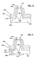
- Figure 8 is a cross-sectional view of yet other embodiments of the present invention that include extended insulating layers and/or electrodes.
- the insulating layer 110' and the second electrode 120' both extend along the substrate face 100a, in addition to extending along the first electrode sidewall 150b. It also will be understood that only one of the insulating layer 110' or the second electrode 120' may extend along the substrate face 100a. Any of the configurations that are described in connection with any of the figures herein may be combined with the extended insulating layer 110' and/or extended second electrode 120' of Figure 8 .
- a second insulating layer 810 also may be provided on the second electrode 120' opposite the insulating layer 110' .
- the second insulating layer 810 may comprise a layer or multiple sublayers comprising silicon dioxide, silicon nitride one or more self-assembled monolayers, one or more polymer films and/or other materials that may be used to protect a device from an outside (ambient) environment.
- the second insulating layer 810 may be a specialized layer that may depend upon the ambient in which a chemically-gated single-electron transistor is being used.
- the second insulating layer 810 may be used with or without the extended layers 110' and 120' of Figure 8 , and/or with any other embodiments that are described in connection with any of the figures herein.
- Figure 9 is a cross-sectional view of other embodiments of the present invention.
- external electrical contacts are provided using a conductive via 910 that electrically connects the second electrode 120' to a pad 920 on the back face of the substrate 100.
- the first electrode 150 also may contact the back face of the substrate 100 at a second pad 930 using internal doped regions of the substrate and/or other conventional techniques.
- Appropriate insulating regions may be provided to electrically insulate the first and second pads 920 and 930 from one another and/or to insulate the conductive via 910 from other regions, using techniques well known to those having skill in the art.
- Solder bumps and/or other interconnect techniques may be used to electrically and/or mechanically connect the first and second contact pads 920 and 930 to an external device. These and other external contact schemes also may be used with any of the described embodiments of the invention.
- Figures 10A-10F are cross-sectional views of single-electron transistors according to embodiments of the present invention, during intermediate fabrication steps according to embodiments of the present invention. These method embodiments may be used to fabricate single-electron transistors as illustrated in Figure 1A . However, similar method embodiments may be used to fabricate single-electron transistors of Figures 1B-9 and/or combinations thereof.
- a mask region 1010 is formed on a substrate 1000, for example by forming a conventional mask comprising silicon nitride on a conventional substrate, and then patterning using conventional photolithography. It will be understood that since the width of the mask region 1010 need not determine the spacing between the first and second electrodes that are formed subsequently, conventional photolithography may be used. It also will be understood that the substrate 1000 may be a conventional substrate, as was described in connection with Figure 1A , such as a layer of doped polysilicon and/or other conductive material on a monocrystalline silicon substrate.
- an anisotropic (wet) etch may be performed using the masking region 1010 as an etching mask, to form the first electrode 150 on a substrate 100.
- Other conventional etching techniques and/or other conventional post-forming techniques such as selective epitaxial growth, may be used.
- the insulating layer 110 is formed, for example by performing a conformal deposition, for example using Chemical Vapor Deposition (CVD), such as Plasma-Enhanced Chemical Vapor Deposition (PECVD), which may not form a continuous insulating layer on the mask region. It also will be understood that the insulating layer 110 also may be formed on the mask region 1010.
- CVD Chemical Vapor Deposition
- PECVD Plasma-Enhanced Chemical Vapor Deposition
- the second electrode 120 is formed on the insulating layer 110, for example using a directional (angled) deposition technique, which may not form a continuous layer on the mask region 1010.
- a directional (angled) deposition technique which may not form a continuous layer on the mask region 1010.
- other deposition techniques may be performed which may also form a conformal layer on the mask region 1010 .
- the mask region 1010 is removed, which may also remove any portions of the insulating layer 110 and/or the second electrode 120 thereon, to thereby define the first electrode end 150a, the insulating layer end 110a, and the second electrode end 120a.
- absorption of the anchoring self-assembled monolayer 130 may be performed, for example, using techniques that were described above.
- At least one nanoparticle 140 then is attached to the anchoring self-assembled monolayer 130, for example, using techniques that were described above.
- Figures 11A-11I are cross-sectional views of other single-electron transistors according to embodiments of the present invention, during intermediate fabrication steps according to embodiments of the present invention.
- a mask region 1010 is formed on a substrate, similar to Figure 10A .
- anisotropic etching and/or other techniques are used to create a first (post) electrode 150, similar to Figure 10B .
- the masking region 1010 then is removed.
- a conformal insulating layer 1110 is formed on the first electrode 150, for example, using conventional conformal deposition techniques. In other embodiments, directional deposition may need not be used.
- a conformal second conductive layer 1120 is formed on the conformal insulating layer 1110, for example using conventional conformal deposition techniques. In other embodiments, directional deposition may not need to be used. Layers 1110 and 1120 may comprise materials that were described earlier for layers 110 and 120, respectively.
- a recessed layer 1130 then may be formed between structures of Figure 11B .
- the recessed layer 1130 may include one or more sublayers comprising silicon dioxide, silicon nitride, polyimide and/or other materials that are compatible with a subsequent selective etching and/or chemical-mechanical polishing process.
- the recessed layer 1130 may be recessed from the top of the conductive layer 1120 by at least the thickness of layers 1110 and 1120. However, smaller or larger recesses also may be provided.
- embodiments of the present invention can provide arrays, including large arrays, of dual concentric electrodes.
- a conducting center electrode and an outer ring electrode can allow electrochemical reactions to be monitored at the apexes of each electrode-insulator-electrode tower.
- the electrodes may be derivatized to include chemical specificity to reactions taking place at the surfaces. Enhanced sensitivity can be made possible by attaching nanometer-sized colloidal particles to the insulating regions between the electrodes, which can create single-electron transistors.
- the colloids can be functionalized with chemically-specific receptors and/or molecules, to incorporate specificity to these reactions.
- Single-electron transistors or arrays thereof may be used, for example, as sensing platforms in the wells of microtiter plates, for biological assays.
- Their enhanced sensitivity compared to conventional larger electrodes can benefit drug discovery and/or biochemistry.
- Their small size also can afford direct insertion of the arrays into living cells, which can allow in vivo chemical study and/or direct mapping of chemical pathways and/or concentrations within the cells.
Landscapes
- Engineering & Computer Science (AREA)
- Chemical & Material Sciences (AREA)
- Nanotechnology (AREA)
- Physics & Mathematics (AREA)
- Health & Medical Sciences (AREA)
- Life Sciences & Earth Sciences (AREA)
- Analytical Chemistry (AREA)
- Pathology (AREA)
- Electrochemistry (AREA)
- Molecular Biology (AREA)
- Microelectronics & Electronic Packaging (AREA)
- Biochemistry (AREA)
- General Health & Medical Sciences (AREA)
- General Physics & Mathematics (AREA)
- Immunology (AREA)
- Chemical Kinetics & Catalysis (AREA)
- Mathematical Physics (AREA)
- Theoretical Computer Science (AREA)
- Crystallography & Structural Chemistry (AREA)
- Thin Film Transistor (AREA)
- Insulated Gate Type Field-Effect Transistor (AREA)
- Bipolar Transistors (AREA)
- Metal-Oxide And Bipolar Metal-Oxide Semiconductor Integrated Circuits (AREA)
Applications Claiming Priority (3)
| Application Number | Priority Date | Filing Date | Title |
|---|---|---|---|
| US905319 | 2001-07-13 | ||
| US09/905,319 US6483125B1 (en) | 2001-07-13 | 2001-07-13 | Single electron transistors in which the thickness of an insulating layer defines spacing between electrodes |
| PCT/US2002/022137 WO2003007384A2 (en) | 2001-07-13 | 2002-07-12 | Single-electron transistors and fabrication methods |
Publications (2)
| Publication Number | Publication Date |
|---|---|
| EP1407492A2 EP1407492A2 (en) | 2004-04-14 |
| EP1407492B1 true EP1407492B1 (en) | 2010-05-19 |
Family
ID=25420626
Family Applications (1)
| Application Number | Title | Priority Date | Filing Date |
|---|---|---|---|
| EP02756451A Expired - Lifetime EP1407492B1 (en) | 2001-07-13 | 2002-07-12 | Single-electron transistors and fabrication methods |
Country Status (8)
| Country | Link |
|---|---|
| US (2) | US6483125B1 (enExample) |
| EP (1) | EP1407492B1 (enExample) |
| JP (1) | JP4814487B2 (enExample) |
| AT (1) | ATE468611T1 (enExample) |
| AU (1) | AU2002322459A1 (enExample) |
| DE (1) | DE60236436D1 (enExample) |
| TW (1) | TW557546B (enExample) |
| WO (1) | WO2003007384A2 (enExample) |
Families Citing this family (30)
| Publication number | Priority date | Publication date | Assignee | Title |
|---|---|---|---|---|
| GB9724642D0 (en) * | 1997-11-21 | 1998-01-21 | British Tech Group | Single electron devices |
| US6653653B2 (en) * | 2001-07-13 | 2003-11-25 | Quantum Logic Devices, Inc. | Single-electron transistors and fabrication methods in which a projecting feature defines spacing between electrodes |
| TW531890B (en) * | 2002-02-27 | 2003-05-11 | Ind Tech Res Inst | Single electron device fabricated from nanoparticle derivatives |
| AU2003247950A1 (en) * | 2002-07-08 | 2004-01-23 | The Regents Of The University Of California | Surface nanopatterning |
| US7224039B1 (en) | 2003-09-09 | 2007-05-29 | International Technology Center | Polymer nanocomposite structures for integrated circuits |
| US8070988B2 (en) * | 2003-09-09 | 2011-12-06 | International Technology Center | Nano-carbon hybrid structures |
| WO2005081707A2 (en) | 2003-11-20 | 2005-09-09 | Biowarn, Llc | Methodology and apparatus for the detection of biological substances |
| KR100671813B1 (ko) * | 2004-10-15 | 2007-01-19 | 세이코 엡슨 가부시키가이샤 | 박막 패턴 형성 방법, 반도체 장치, 전기 광학 장치, 및전자 기기 |
| JP4297106B2 (ja) * | 2005-02-23 | 2009-07-15 | セイコーエプソン株式会社 | 膜パターンの形成方法及びデバイスの製造方法、電気光学装置及び電子機器 |
| US7309650B1 (en) | 2005-02-24 | 2007-12-18 | Spansion Llc | Memory device having a nanocrystal charge storage region and method |
| US7378310B1 (en) | 2005-04-27 | 2008-05-27 | Spansion Llc | Method for manufacturing a memory device having a nanocrystal charge storage region |
| US7335594B1 (en) | 2005-04-27 | 2008-02-26 | Spansion Llc | Method for manufacturing a memory device having a nanocrystal charge storage region |
| JP4613314B2 (ja) * | 2005-05-26 | 2011-01-19 | 独立行政法人産業技術総合研究所 | 単結晶の製造方法 |
| US20070202648A1 (en) * | 2006-02-28 | 2007-08-30 | Samsung Electronics Co. Ltd. | Memory device and method of manufacturing the same |
| US8507894B2 (en) * | 2008-02-11 | 2013-08-13 | Qucor Pty Limited | Control and readout of electron or hole spin |
| WO2010025547A1 (en) * | 2008-09-02 | 2010-03-11 | The Governing Council Of The University Of Toronto | Nanostructured microelectrodes and biosensing devices incorporating the same |
| EP3314245A4 (en) | 2015-06-25 | 2019-02-27 | Roswell Biotechnologies, Inc | BIOMOLECULAR SENSORS AND METHOD |
| EP4137808A1 (en) | 2016-01-28 | 2023-02-22 | Roswell Biotechnologies, Inc. | Method of making a sequencing device |
| JP7280590B2 (ja) | 2016-01-28 | 2023-05-24 | ロズウェル バイオテクノロジーズ,インコーポレイテッド | 大スケールの分子電子工学センサアレイを使用する被分析物を測定するための方法および装置 |
| KR102734671B1 (ko) | 2016-02-09 | 2024-11-25 | 로스웰 엠이 아이엔씨. | 전자 비표지 dna 및 게놈 시퀀싱 |
| US10597767B2 (en) | 2016-02-22 | 2020-03-24 | Roswell Biotechnologies, Inc. | Nanoparticle fabrication |
| US9829456B1 (en) * | 2016-07-26 | 2017-11-28 | Roswell Biotechnologies, Inc. | Method of making a multi-electrode structure usable in molecular sensing devices |
| CA3052062A1 (en) | 2017-01-10 | 2018-07-19 | Roswell Biotechnologies, Inc. | Methods and systems for dna data storage |
| WO2018136148A1 (en) | 2017-01-19 | 2018-07-26 | Roswell Biotechnologies, Inc. | Solid state sequencing devices comprising two dimensional layer materials |
| US10508296B2 (en) | 2017-04-25 | 2019-12-17 | Roswell Biotechnologies, Inc. | Enzymatic circuits for molecular sensors |
| EP3615685B1 (en) | 2017-04-25 | 2025-02-19 | Roswell Biotechnologies, Inc | Enzymatic circuits for molecular sensors |
| CA3057155A1 (en) | 2017-05-09 | 2018-11-15 | Roswell Biotechnologies, Inc. | Binding probe circuits for molecular sensors |
| US11371955B2 (en) | 2017-08-30 | 2022-06-28 | Roswell Biotechnologies, Inc. | Processive enzyme molecular electronic sensors for DNA data storage |
| CN111373051A (zh) | 2017-10-10 | 2020-07-03 | 罗斯威尔生命技术公司 | 用于无扩增dna数据存储的方法、装置和系统 |
| US12146852B2 (en) | 2019-09-06 | 2024-11-19 | Roswell Biotechnologies, Inc. | Methods of fabricating nanoscale structures usable in molecular sensors and other devices |
Family Cites Families (35)
| Publication number | Priority date | Publication date | Assignee | Title |
|---|---|---|---|---|
| GB8406955D0 (en) | 1984-03-16 | 1984-04-18 | Serono Diagnostics Ltd | Assay |
| DE3513168A1 (de) | 1985-04-12 | 1986-10-16 | Thomas 8000 München Dandekar | Biosensor bestehend aus einem halbleiter auf silizium oder kohlenstoffbasis (elektronischer teil) und nukleinbasen (od. anderen biol. monomeren) |
| US4894339A (en) | 1985-12-18 | 1990-01-16 | Seitaikinouriyou Kagakuhin Sinseizogijutsu Kenkyu Kumiai | Immobilized enzyme membrane for a semiconductor sensor |
| JPS6350745A (ja) | 1986-08-20 | 1988-03-03 | Fuji Photo Film Co Ltd | 化学センサ− |
| DE3827314C1 (enExample) | 1988-08-11 | 1989-10-19 | Christoff Prof. Dr. Braeuchle | |
| US5219577A (en) | 1990-06-22 | 1993-06-15 | The Regents Of The University Of California | Biologically active composition having a nanocrystalline core |
| WO1993008464A1 (en) | 1991-10-21 | 1993-04-29 | Holm Kennedy James W | Method and device for biochemical sensing |
| US5846708A (en) | 1991-11-19 | 1998-12-08 | Massachusetts Institiute Of Technology | Optical and electrical methods and apparatus for molecule detection |
| US5405454A (en) * | 1992-03-19 | 1995-04-11 | Matsushita Electric Industrial Co., Ltd. | Electrically insulated silicon structure and producing method therefor |
| US5420746A (en) | 1993-04-13 | 1995-05-30 | The United States Of America As Represented By The Secretary Of The Army | Single electron device including clusters of pure carbon atoms |
| DE59502654D1 (de) * | 1994-04-19 | 1998-07-30 | Siemens Ag | Mikroelektronisches bauelement und verfahren zu dessen herstellung |
| JPH0878669A (ja) * | 1994-09-02 | 1996-03-22 | Hitachi Ltd | 半導体装置および半導体装置の製造方法 |
| JP3149718B2 (ja) | 1995-02-03 | 2001-03-26 | 松下電器産業株式会社 | 単電子トランジスタ |
| US5576563A (en) | 1995-04-24 | 1996-11-19 | Motorola Inc. | Chemical probe field effect transistor for measuring the surface potential of a gate electrode in response to chemical exposure |
| DE19522351A1 (de) * | 1995-06-20 | 1997-01-09 | Max Planck Gesellschaft | Verfahren zur Herstellung von Quantenstrukturen, insbesondere von Quantenpunkten und Tunnelbarrieren sowie Bauelemente mit solchen Quantenstrukturen |
| US6057556A (en) | 1996-03-26 | 2000-05-02 | Samsung Electronics Co., Ltd. | Tunneling device and method of producing a tunneling device |
| DE19621994C1 (de) | 1996-05-31 | 1997-06-12 | Siemens Ag | Einzelelektron-Speicherzellenanordnung |
| US6066265A (en) | 1996-06-19 | 2000-05-23 | Kionix, Inc. | Micromachined silicon probe for scanning probe microscopy |
| US5747839A (en) | 1996-09-30 | 1998-05-05 | Motorola, Inc. | Chemical sensing trench field effect transistor |
| US5922537A (en) | 1996-11-08 | 1999-07-13 | N.o slashed.AB Immunoassay, Inc. | Nanoparticles biosensor |
| US6103868A (en) | 1996-12-27 | 2000-08-15 | The Regents Of The University Of California | Organically-functionalized monodisperse nanocrystals of metals |
| EP0865078A1 (en) | 1997-03-13 | 1998-09-16 | Hitachi Europe Limited | Method of depositing nanometre scale particles |
| US5900728A (en) | 1997-03-20 | 1999-05-04 | International Business Machines Corporation | Alternating current magnetic force microscopy system with probe having integrated coil |
| US5900729A (en) | 1997-03-20 | 1999-05-04 | International Business Machines Corporation | Magnetic force microscopy probe with integrated coil |
| US6159620A (en) | 1997-03-31 | 2000-12-12 | The Regents Of The University Of California | Single-electron solid state electronic device |
| EP1154493A3 (en) | 1997-05-30 | 2003-10-15 | Matsushita Electric Industrial Co., Ltd. | Light-emitting semiconductor device having quantum dots |
| KR100223807B1 (ko) * | 1997-06-04 | 1999-10-15 | 구본준 | 반도체 소자의 제조방법 |
| JP3452764B2 (ja) * | 1997-06-11 | 2003-09-29 | 科学技術振興事業団 | 超微細突起構造体の製造方法 |
| US5892252A (en) | 1998-02-05 | 1999-04-06 | Motorola, Inc. | Chemical sensing trench field effect transistor and method for same |
| EP1073902A2 (en) | 1998-04-20 | 2001-02-07 | University Of North Carolina At Chapel Hill | Nanometer particles containing a reactive monolayer |
| US6211530B1 (en) * | 1998-06-12 | 2001-04-03 | Motorola, Inc. | Sparse-carrier devices and method of fabrication |
| US6218175B1 (en) * | 1998-10-30 | 2001-04-17 | International Business Machines Corporation | Nano-devices using block-copolymers |
| JP2000349275A (ja) * | 1999-06-01 | 2000-12-15 | Nec Corp | 単一電子素子とその製造方法 |
| AU7700600A (en) * | 1999-08-18 | 2001-03-13 | North Carolina State University | Sensing devices using chemically-gated single electron transistors |
| US6410934B1 (en) * | 2001-02-09 | 2002-06-25 | The Board Of Trustees Of The University Of Illinois | Silicon nanoparticle electronic switches |
-
2001
- 2001-07-13 US US09/905,319 patent/US6483125B1/en not_active Expired - Fee Related
-
2002
- 2002-07-12 TW TW091115527A patent/TW557546B/zh active
- 2002-07-12 AT AT02756451T patent/ATE468611T1/de not_active IP Right Cessation
- 2002-07-12 EP EP02756451A patent/EP1407492B1/en not_active Expired - Lifetime
- 2002-07-12 WO PCT/US2002/022137 patent/WO2003007384A2/en not_active Ceased
- 2002-07-12 DE DE60236436T patent/DE60236436D1/de not_active Expired - Fee Related
- 2002-07-12 AU AU2002322459A patent/AU2002322459A1/en not_active Abandoned
- 2002-07-12 JP JP2003513046A patent/JP4814487B2/ja not_active Expired - Fee Related
- 2002-09-17 US US10/244,860 patent/US6784082B2/en not_active Expired - Fee Related
Also Published As
| Publication number | Publication date |
|---|---|
| US20030025133A1 (en) | 2003-02-06 |
| JP2005526371A (ja) | 2005-09-02 |
| AU2002322459A1 (en) | 2003-01-29 |
| US6784082B2 (en) | 2004-08-31 |
| ATE468611T1 (de) | 2010-06-15 |
| WO2003007384A2 (en) | 2003-01-23 |
| JP4814487B2 (ja) | 2011-11-16 |
| EP1407492A2 (en) | 2004-04-14 |
| US6483125B1 (en) | 2002-11-19 |
| DE60236436D1 (de) | 2010-07-01 |
| TW557546B (en) | 2003-10-11 |
| WO2003007384A3 (en) | 2003-05-08 |
Similar Documents
| Publication | Publication Date | Title |
|---|---|---|
| EP1407492B1 (en) | Single-electron transistors and fabrication methods | |
| EP1407493B1 (en) | Single-electron transistors and fabrication methods in which a projecting feature defines spacing between electrodes | |
| US6891227B2 (en) | Self-aligned nanotube field effect transistor and method of fabricating same | |
| US7892956B2 (en) | Methods of manufacture of vertical nanowire FET devices | |
| US7922927B2 (en) | Method of forming one or more nanopores for aligning molecules for molecular electronics | |
| JP5511746B2 (ja) | 垂直型ナノチューブ半導体デバイス構造体の形成方法 | |
| KR100992296B1 (ko) | 어레이 배열로 수직 탄소 나노튜브 전계 효과 트랜지스터를 제조하는 방법 및 이에 의해 형성된 전계 효과 트랜지스터와 어레이 | |
| JP2010506735A (ja) | 低次元構造体のカプセル化、転移方法 | |
| US6673717B1 (en) | Methods for fabricating nanopores for single-electron devices | |
| US7208784B2 (en) | Single-electron transistor for detecting biomolecules |
Legal Events
| Date | Code | Title | Description |
|---|---|---|---|
| PUAI | Public reference made under article 153(3) epc to a published international application that has entered the european phase |
Free format text: ORIGINAL CODE: 0009012 |
|
| 17P | Request for examination filed |
Effective date: 20040112 |
|
| AK | Designated contracting states |
Kind code of ref document: A2 Designated state(s): AT BE BG CH CY CZ DE DK EE ES FI FR GB GR IE IT LI LU MC NL PT SE SK TR |
|
| AX | Request for extension of the european patent |
Extension state: AL LT LV MK RO SI |
|
| 17Q | First examination report despatched |
Effective date: 20051207 |
|
| GRAP | Despatch of communication of intention to grant a patent |
Free format text: ORIGINAL CODE: EPIDOSNIGR1 |
|
| GRAS | Grant fee paid |
Free format text: ORIGINAL CODE: EPIDOSNIGR3 |
|
| GRAA | (expected) grant |
Free format text: ORIGINAL CODE: 0009210 |
|
| AK | Designated contracting states |
Kind code of ref document: B1 Designated state(s): AT BE BG CH CY CZ DE DK EE ES FI FR GB GR IE IT LI LU MC NL PT SE SK TR |
|
| REG | Reference to a national code |
Ref country code: GB Ref legal event code: FG4D |
|
| REG | Reference to a national code |
Ref country code: CH Ref legal event code: EP |
|
| REG | Reference to a national code |
Ref country code: IE Ref legal event code: FG4D |
|
| REF | Corresponds to: |
Ref document number: 60236436 Country of ref document: DE Date of ref document: 20100701 Kind code of ref document: P |
|
| REG | Reference to a national code |
Ref country code: NL Ref legal event code: VDEP Effective date: 20100519 |
|
| PG25 | Lapsed in a contracting state [announced via postgrant information from national office to epo] |
Ref country code: SE Free format text: LAPSE BECAUSE OF FAILURE TO SUBMIT A TRANSLATION OF THE DESCRIPTION OR TO PAY THE FEE WITHIN THE PRESCRIBED TIME-LIMIT Effective date: 20100519 Ref country code: ES Free format text: LAPSE BECAUSE OF FAILURE TO SUBMIT A TRANSLATION OF THE DESCRIPTION OR TO PAY THE FEE WITHIN THE PRESCRIBED TIME-LIMIT Effective date: 20100830 |
|
| PG25 | Lapsed in a contracting state [announced via postgrant information from national office to epo] |
Ref country code: AT Free format text: LAPSE BECAUSE OF FAILURE TO SUBMIT A TRANSLATION OF THE DESCRIPTION OR TO PAY THE FEE WITHIN THE PRESCRIBED TIME-LIMIT Effective date: 20100519 Ref country code: FI Free format text: LAPSE BECAUSE OF FAILURE TO SUBMIT A TRANSLATION OF THE DESCRIPTION OR TO PAY THE FEE WITHIN THE PRESCRIBED TIME-LIMIT Effective date: 20100519 |
|
| PG25 | Lapsed in a contracting state [announced via postgrant information from national office to epo] |
Ref country code: GR Free format text: LAPSE BECAUSE OF FAILURE TO SUBMIT A TRANSLATION OF THE DESCRIPTION OR TO PAY THE FEE WITHIN THE PRESCRIBED TIME-LIMIT Effective date: 20100820 Ref country code: CY Free format text: LAPSE BECAUSE OF FAILURE TO SUBMIT A TRANSLATION OF THE DESCRIPTION OR TO PAY THE FEE WITHIN THE PRESCRIBED TIME-LIMIT Effective date: 20100519 |
|
| PG25 | Lapsed in a contracting state [announced via postgrant information from national office to epo] |
Ref country code: DK Free format text: LAPSE BECAUSE OF FAILURE TO SUBMIT A TRANSLATION OF THE DESCRIPTION OR TO PAY THE FEE WITHIN THE PRESCRIBED TIME-LIMIT Effective date: 20100519 Ref country code: PT Free format text: LAPSE BECAUSE OF FAILURE TO SUBMIT A TRANSLATION OF THE DESCRIPTION OR TO PAY THE FEE WITHIN THE PRESCRIBED TIME-LIMIT Effective date: 20100920 Ref country code: NL Free format text: LAPSE BECAUSE OF FAILURE TO SUBMIT A TRANSLATION OF THE DESCRIPTION OR TO PAY THE FEE WITHIN THE PRESCRIBED TIME-LIMIT Effective date: 20100519 Ref country code: EE Free format text: LAPSE BECAUSE OF FAILURE TO SUBMIT A TRANSLATION OF THE DESCRIPTION OR TO PAY THE FEE WITHIN THE PRESCRIBED TIME-LIMIT Effective date: 20100519 |
|
| PG25 | Lapsed in a contracting state [announced via postgrant information from national office to epo] |
Ref country code: SK Free format text: LAPSE BECAUSE OF FAILURE TO SUBMIT A TRANSLATION OF THE DESCRIPTION OR TO PAY THE FEE WITHIN THE PRESCRIBED TIME-LIMIT Effective date: 20100519 Ref country code: CZ Free format text: LAPSE BECAUSE OF FAILURE TO SUBMIT A TRANSLATION OF THE DESCRIPTION OR TO PAY THE FEE WITHIN THE PRESCRIBED TIME-LIMIT Effective date: 20100519 Ref country code: MC Free format text: LAPSE BECAUSE OF NON-PAYMENT OF DUE FEES Effective date: 20100731 Ref country code: BE Free format text: LAPSE BECAUSE OF FAILURE TO SUBMIT A TRANSLATION OF THE DESCRIPTION OR TO PAY THE FEE WITHIN THE PRESCRIBED TIME-LIMIT Effective date: 20100519 |
|
| REG | Reference to a national code |
Ref country code: CH Ref legal event code: PL |
|
| PLBE | No opposition filed within time limit |
Free format text: ORIGINAL CODE: 0009261 |
|
| STAA | Information on the status of an ep patent application or granted ep patent |
Free format text: STATUS: NO OPPOSITION FILED WITHIN TIME LIMIT |
|
| PG25 | Lapsed in a contracting state [announced via postgrant information from national office to epo] |
Ref country code: IT Free format text: LAPSE BECAUSE OF FAILURE TO SUBMIT A TRANSLATION OF THE DESCRIPTION OR TO PAY THE FEE WITHIN THE PRESCRIBED TIME-LIMIT Effective date: 20100519 |
|
| REG | Reference to a national code |
Ref country code: FR Ref legal event code: ST Effective date: 20110331 |
|
| 26N | No opposition filed |
Effective date: 20110222 |
|
| GBPC | Gb: european patent ceased through non-payment of renewal fee |
Effective date: 20100819 |
|
| PG25 | Lapsed in a contracting state [announced via postgrant information from national office to epo] |
Ref country code: LI Free format text: LAPSE BECAUSE OF NON-PAYMENT OF DUE FEES Effective date: 20100731 Ref country code: CH Free format text: LAPSE BECAUSE OF NON-PAYMENT OF DUE FEES Effective date: 20100731 Ref country code: DE Free format text: LAPSE BECAUSE OF NON-PAYMENT OF DUE FEES Effective date: 20110201 |
|
| REG | Reference to a national code |
Ref country code: DE Ref legal event code: R119 Ref document number: 60236436 Country of ref document: DE Effective date: 20110201 |
|
| PG25 | Lapsed in a contracting state [announced via postgrant information from national office to epo] |
Ref country code: FR Free format text: LAPSE BECAUSE OF NON-PAYMENT OF DUE FEES Effective date: 20100802 |
|
| PG25 | Lapsed in a contracting state [announced via postgrant information from national office to epo] |
Ref country code: IE Free format text: LAPSE BECAUSE OF NON-PAYMENT OF DUE FEES Effective date: 20100712 |
|
| PG25 | Lapsed in a contracting state [announced via postgrant information from national office to epo] |
Ref country code: GB Free format text: LAPSE BECAUSE OF NON-PAYMENT OF DUE FEES Effective date: 20100819 |
|
| REG | Reference to a national code |
Ref country code: DE Ref legal event code: R097 Ref document number: 60236436 Country of ref document: DE Effective date: 20110222 |
|
| PG25 | Lapsed in a contracting state [announced via postgrant information from national office to epo] |
Ref country code: LU Free format text: LAPSE BECAUSE OF NON-PAYMENT OF DUE FEES Effective date: 20100712 Ref country code: BG Free format text: LAPSE BECAUSE OF FAILURE TO SUBMIT A TRANSLATION OF THE DESCRIPTION OR TO PAY THE FEE WITHIN THE PRESCRIBED TIME-LIMIT Effective date: 20100519 |
|
| PG25 | Lapsed in a contracting state [announced via postgrant information from national office to epo] |
Ref country code: TR Free format text: LAPSE BECAUSE OF FAILURE TO SUBMIT A TRANSLATION OF THE DESCRIPTION OR TO PAY THE FEE WITHIN THE PRESCRIBED TIME-LIMIT Effective date: 20100519 |
|
| PG25 | Lapsed in a contracting state [announced via postgrant information from national office to epo] |
Ref country code: BG Free format text: LAPSE BECAUSE OF FAILURE TO SUBMIT A TRANSLATION OF THE DESCRIPTION OR TO PAY THE FEE WITHIN THE PRESCRIBED TIME-LIMIT Effective date: 20100819 |