US11371955B2 - Processive enzyme molecular electronic sensors for DNA data storage - Google Patents
Processive enzyme molecular electronic sensors for DNA data storage Download PDFInfo
- Publication number
- US11371955B2 US11371955B2 US16/639,716 US201816639716A US11371955B2 US 11371955 B2 US11371955 B2 US 11371955B2 US 201816639716 A US201816639716 A US 201816639716A US 11371955 B2 US11371955 B2 US 11371955B2
- Authority
- US
- United States
- Prior art keywords
- dna
- electrode
- sensor
- molecule
- processive enzyme
- Prior art date
- Legal status (The legal status is an assumption and is not a legal conclusion. Google has not performed a legal analysis and makes no representation as to the accuracy of the status listed.)
- Active
Links
- 102000004190 Enzymes Human genes 0.000 title claims abstract description 293
- 108090000790 Enzymes Proteins 0.000 title claims abstract description 293
- 238000013500 data storage Methods 0.000 title abstract description 25
- 238000005442 molecular electronic Methods 0.000 title description 32
- 108020004414 DNA Proteins 0.000 claims abstract description 398
- 102000053602 DNA Human genes 0.000 claims abstract description 108
- 108060004795 Methyltransferase Proteins 0.000 claims description 42
- 102000004169 proteins and genes Human genes 0.000 claims description 26
- 108090000623 proteins and genes Proteins 0.000 claims description 26
- 108060002716 Exonuclease Proteins 0.000 claims description 25
- 102000013165 exonuclease Human genes 0.000 claims description 25
- 238000004806 packaging method and process Methods 0.000 claims description 12
- 102100034343 Integrase Human genes 0.000 claims description 7
- 108010092799 RNA-directed DNA polymerase Proteins 0.000 claims description 7
- 108020005202 Viral DNA Proteins 0.000 claims description 6
- 230000037361 pathway Effects 0.000 claims description 5
- 238000000034 method Methods 0.000 abstract description 91
- 230000008569 process Effects 0.000 abstract description 36
- 239000000284 extract Substances 0.000 abstract description 3
- 238000013075 data extraction Methods 0.000 abstract description 2
- 238000002360 preparation method Methods 0.000 abstract description 2
- 229940088598 enzyme Drugs 0.000 description 285
- 108091034117 Oligonucleotide Proteins 0.000 description 97
- JLCPHMBAVCMARE-UHFFFAOYSA-N [3-[[3-[[3-[[3-[[3-[[3-[[3-[[3-[[3-[[3-[[3-[[5-(2-amino-6-oxo-1H-purin-9-yl)-3-[[3-[[3-[[3-[[3-[[3-[[5-(2-amino-6-oxo-1H-purin-9-yl)-3-[[5-(2-amino-6-oxo-1H-purin-9-yl)-3-hydroxyoxolan-2-yl]methoxy-hydroxyphosphoryl]oxyoxolan-2-yl]methoxy-hydroxyphosphoryl]oxy-5-(5-methyl-2,4-dioxopyrimidin-1-yl)oxolan-2-yl]methoxy-hydroxyphosphoryl]oxy-5-(6-aminopurin-9-yl)oxolan-2-yl]methoxy-hydroxyphosphoryl]oxy-5-(6-aminopurin-9-yl)oxolan-2-yl]methoxy-hydroxyphosphoryl]oxy-5-(6-aminopurin-9-yl)oxolan-2-yl]methoxy-hydroxyphosphoryl]oxy-5-(6-aminopurin-9-yl)oxolan-2-yl]methoxy-hydroxyphosphoryl]oxyoxolan-2-yl]methoxy-hydroxyphosphoryl]oxy-5-(5-methyl-2,4-dioxopyrimidin-1-yl)oxolan-2-yl]methoxy-hydroxyphosphoryl]oxy-5-(4-amino-2-oxopyrimidin-1-yl)oxolan-2-yl]methoxy-hydroxyphosphoryl]oxy-5-(5-methyl-2,4-dioxopyrimidin-1-yl)oxolan-2-yl]methoxy-hydroxyphosphoryl]oxy-5-(5-methyl-2,4-dioxopyrimidin-1-yl)oxolan-2-yl]methoxy-hydroxyphosphoryl]oxy-5-(6-aminopurin-9-yl)oxolan-2-yl]methoxy-hydroxyphosphoryl]oxy-5-(6-aminopurin-9-yl)oxolan-2-yl]methoxy-hydroxyphosphoryl]oxy-5-(4-amino-2-oxopyrimidin-1-yl)oxolan-2-yl]methoxy-hydroxyphosphoryl]oxy-5-(4-amino-2-oxopyrimidin-1-yl)oxolan-2-yl]methoxy-hydroxyphosphoryl]oxy-5-(4-amino-2-oxopyrimidin-1-yl)oxolan-2-yl]methoxy-hydroxyphosphoryl]oxy-5-(6-aminopurin-9-yl)oxolan-2-yl]methoxy-hydroxyphosphoryl]oxy-5-(4-amino-2-oxopyrimidin-1-yl)oxolan-2-yl]methyl [5-(6-aminopurin-9-yl)-2-(hydroxymethyl)oxolan-3-yl] hydrogen phosphate Polymers Cc1cn(C2CC(OP(O)(=O)OCC3OC(CC3OP(O)(=O)OCC3OC(CC3O)n3cnc4c3nc(N)[nH]c4=O)n3cnc4c3nc(N)[nH]c4=O)C(COP(O)(=O)OC3CC(OC3COP(O)(=O)OC3CC(OC3COP(O)(=O)OC3CC(OC3COP(O)(=O)OC3CC(OC3COP(O)(=O)OC3CC(OC3COP(O)(=O)OC3CC(OC3COP(O)(=O)OC3CC(OC3COP(O)(=O)OC3CC(OC3COP(O)(=O)OC3CC(OC3COP(O)(=O)OC3CC(OC3COP(O)(=O)OC3CC(OC3COP(O)(=O)OC3CC(OC3COP(O)(=O)OC3CC(OC3COP(O)(=O)OC3CC(OC3COP(O)(=O)OC3CC(OC3COP(O)(=O)OC3CC(OC3COP(O)(=O)OC3CC(OC3CO)n3cnc4c(N)ncnc34)n3ccc(N)nc3=O)n3cnc4c(N)ncnc34)n3ccc(N)nc3=O)n3ccc(N)nc3=O)n3ccc(N)nc3=O)n3cnc4c(N)ncnc34)n3cnc4c(N)ncnc34)n3cc(C)c(=O)[nH]c3=O)n3cc(C)c(=O)[nH]c3=O)n3ccc(N)nc3=O)n3cc(C)c(=O)[nH]c3=O)n3cnc4c3nc(N)[nH]c4=O)n3cnc4c(N)ncnc34)n3cnc4c(N)ncnc34)n3cnc4c(N)ncnc34)n3cnc4c(N)ncnc34)O2)c(=O)[nH]c1=O JLCPHMBAVCMARE-UHFFFAOYSA-N 0.000 description 70
- 230000011664 signaling Effects 0.000 description 57
- 230000021615 conjugation Effects 0.000 description 49
- 238000005259 measurement Methods 0.000 description 34
- 239000000872 buffer Substances 0.000 description 27
- 230000003094 perturbing effect Effects 0.000 description 26
- 239000000243 solution Substances 0.000 description 24
- OKTJSMMVPCPJKN-UHFFFAOYSA-N Carbon Chemical compound [C] OKTJSMMVPCPJKN-UHFFFAOYSA-N 0.000 description 23
- 230000027455 binding Effects 0.000 description 23
- 238000003860 storage Methods 0.000 description 23
- 235000018102 proteins Nutrition 0.000 description 22
- 239000000758 substrate Substances 0.000 description 22
- 238000012545 processing Methods 0.000 description 20
- 230000000694 effects Effects 0.000 description 19
- 239000011148 porous material Substances 0.000 description 18
- 238000006073 displacement reaction Methods 0.000 description 17
- 230000000295 complement effect Effects 0.000 description 16
- 238000012986 modification Methods 0.000 description 16
- 239000002041 carbon nanotube Substances 0.000 description 15
- 229910021393 carbon nanotube Inorganic materials 0.000 description 15
- 230000004048 modification Effects 0.000 description 15
- 125000003636 chemical group Chemical group 0.000 description 13
- 230000008878 coupling Effects 0.000 description 13
- 238000010168 coupling process Methods 0.000 description 13
- 238000005859 coupling reaction Methods 0.000 description 13
- PCHJSUWPFVWCPO-UHFFFAOYSA-N gold Chemical compound [Au] PCHJSUWPFVWCPO-UHFFFAOYSA-N 0.000 description 13
- 150000002500 ions Chemical class 0.000 description 13
- 238000004519 manufacturing process Methods 0.000 description 13
- 229910052737 gold Inorganic materials 0.000 description 12
- 239000010931 gold Substances 0.000 description 12
- 230000003993 interaction Effects 0.000 description 12
- 239000012528 membrane Substances 0.000 description 12
- 229920000642 polymer Polymers 0.000 description 12
- 108020004682 Single-Stranded DNA Proteins 0.000 description 11
- 108090000765 processed proteins & peptides Proteins 0.000 description 11
- 230000008901 benefit Effects 0.000 description 10
- 239000003153 chemical reaction reagent Substances 0.000 description 10
- 239000000126 substance Substances 0.000 description 10
- 230000003287 optical effect Effects 0.000 description 9
- 102000004196 processed proteins & peptides Human genes 0.000 description 9
- 229910019142 PO4 Inorganic materials 0.000 description 8
- 108091028043 Nucleic acid sequence Proteins 0.000 description 7
- 230000015572 biosynthetic process Effects 0.000 description 7
- 239000000463 material Substances 0.000 description 7
- -1 nucleotide phosphoramidite Chemical class 0.000 description 7
- 235000021317 phosphate Nutrition 0.000 description 7
- 238000003786 synthesis reaction Methods 0.000 description 7
- 230000003682 DNA packaging effect Effects 0.000 description 6
- 238000009396 hybridization Methods 0.000 description 6
- 125000002467 phosphate group Chemical group [H]OP(=O)(O[H])O[*] 0.000 description 6
- BASFCYQUMIYNBI-UHFFFAOYSA-N platinum Chemical compound [Pt] BASFCYQUMIYNBI-UHFFFAOYSA-N 0.000 description 6
- 238000011084 recovery Methods 0.000 description 6
- 238000006243 chemical reaction Methods 0.000 description 5
- 229910052804 chromium Inorganic materials 0.000 description 5
- 239000011651 chromium Substances 0.000 description 5
- 238000012937 correction Methods 0.000 description 5
- 238000013461 design Methods 0.000 description 5
- 230000006870 function Effects 0.000 description 5
- 229910021389 graphene Inorganic materials 0.000 description 5
- 239000000203 mixture Substances 0.000 description 5
- 239000002074 nanoribbon Substances 0.000 description 5
- 239000002071 nanotube Substances 0.000 description 5
- 102000039446 nucleic acids Human genes 0.000 description 5
- 108020004707 nucleic acids Proteins 0.000 description 5
- 150000003013 phosphoric acid derivatives Chemical class 0.000 description 5
- 230000006820 DNA synthesis Effects 0.000 description 4
- 239000002202 Polyethylene glycol Substances 0.000 description 4
- 230000009471 action Effects 0.000 description 4
- 230000003321 amplification Effects 0.000 description 4
- 210000003484 anatomy Anatomy 0.000 description 4
- 239000007853 buffer solution Substances 0.000 description 4
- 239000003990 capacitor Substances 0.000 description 4
- 239000010410 layer Substances 0.000 description 4
- 229910052751 metal Inorganic materials 0.000 description 4
- 239000002184 metal Substances 0.000 description 4
- 239000002070 nanowire Substances 0.000 description 4
- 238000003199 nucleic acid amplification method Methods 0.000 description 4
- 150000007523 nucleic acids Chemical class 0.000 description 4
- 229920001223 polyethylene glycol Polymers 0.000 description 4
- 239000004065 semiconductor Substances 0.000 description 4
- 238000013519 translation Methods 0.000 description 4
- 230000005945 translocation Effects 0.000 description 4
- 102100027447 ATP-dependent DNA helicase Q1 Human genes 0.000 description 3
- VYZAMTAEIAYCRO-UHFFFAOYSA-N Chromium Chemical compound [Cr] VYZAMTAEIAYCRO-UHFFFAOYSA-N 0.000 description 3
- 102000004594 DNA Polymerase I Human genes 0.000 description 3
- 108010017826 DNA Polymerase I Proteins 0.000 description 3
- IAZDPXIOMUYVGZ-UHFFFAOYSA-N Dimethylsulphoxide Chemical compound CS(C)=O IAZDPXIOMUYVGZ-UHFFFAOYSA-N 0.000 description 3
- 101000580659 Homo sapiens ATP-dependent DNA helicase Q1 Proteins 0.000 description 3
- 102000016943 Muramidase Human genes 0.000 description 3
- 108010014251 Muramidase Proteins 0.000 description 3
- MSFSPUZXLOGKHJ-UHFFFAOYSA-N Muraminsaeure Natural products OC(=O)C(C)OC1C(N)C(O)OC(CO)C1O MSFSPUZXLOGKHJ-UHFFFAOYSA-N 0.000 description 3
- 108010062010 N-Acetylmuramoyl-L-alanine Amidase Proteins 0.000 description 3
- 108091093037 Peptide nucleic acid Proteins 0.000 description 3
- 108010013639 Peptidoglycan Proteins 0.000 description 3
- XUIMIQQOPSSXEZ-UHFFFAOYSA-N Silicon Chemical compound [Si] XUIMIQQOPSSXEZ-UHFFFAOYSA-N 0.000 description 3
- HEMHJVSKTPXQMS-UHFFFAOYSA-M Sodium hydroxide Chemical compound [OH-].[Na+] HEMHJVSKTPXQMS-UHFFFAOYSA-M 0.000 description 3
- 108010090804 Streptavidin Proteins 0.000 description 3
- 150000001413 amino acids Chemical class 0.000 description 3
- BBEAQIROQSPTKN-UHFFFAOYSA-N antipyrene Natural products C1=CC=C2C=CC3=CC=CC4=CC=C1C2=C43 BBEAQIROQSPTKN-UHFFFAOYSA-N 0.000 description 3
- 230000009286 beneficial effect Effects 0.000 description 3
- 230000001268 conjugating effect Effects 0.000 description 3
- 230000029087 digestion Effects 0.000 description 3
- 230000002708 enhancing effect Effects 0.000 description 3
- 230000002255 enzymatic effect Effects 0.000 description 3
- 230000005284 excitation Effects 0.000 description 3
- 230000002068 genetic effect Effects 0.000 description 3
- 230000000977 initiatory effect Effects 0.000 description 3
- 230000033001 locomotion Effects 0.000 description 3
- 239000010452 phosphate Substances 0.000 description 3
- 229910052697 platinum Inorganic materials 0.000 description 3
- 150000003839 salts Chemical class 0.000 description 3
- 238000001338 self-assembly Methods 0.000 description 3
- 239000010703 silicon Substances 0.000 description 3
- 229910052710 silicon Inorganic materials 0.000 description 3
- 239000007787 solid Substances 0.000 description 3
- 241000894007 species Species 0.000 description 3
- 238000001228 spectrum Methods 0.000 description 3
- 238000012546 transfer Methods 0.000 description 3
- 235000011178 triphosphate Nutrition 0.000 description 3
- 239000001226 triphosphate Substances 0.000 description 3
- YBJHBAHKTGYVGT-ZKWXMUAHSA-N (+)-Biotin Chemical compound N1C(=O)N[C@@H]2[C@H](CCCCC(=O)O)SC[C@@H]21 YBJHBAHKTGYVGT-ZKWXMUAHSA-N 0.000 description 2
- 108090000133 DNA helicases Proteins 0.000 description 2
- 102000003844 DNA helicases Human genes 0.000 description 2
- 108010007577 Exodeoxyribonuclease I Proteins 0.000 description 2
- XZWYTXMRWQJBGX-VXBMVYAYSA-N FLAG peptide Chemical compound NCCCC[C@@H](C(O)=O)NC(=O)[C@H](CC(O)=O)NC(=O)[C@H](CC(O)=O)NC(=O)[C@H](CC(O)=O)NC(=O)[C@H](CC(O)=O)NC(=O)[C@H](CCCCN)NC(=O)[C@@H](NC(=O)[C@@H](N)CC(O)=O)CC1=CC=C(O)C=C1 XZWYTXMRWQJBGX-VXBMVYAYSA-N 0.000 description 2
- 108010020195 FLAG peptide Proteins 0.000 description 2
- 108091093094 Glycol nucleic acid Proteins 0.000 description 2
- ZRALSGWEFCBTJO-UHFFFAOYSA-N Guanidine Chemical compound NC(N)=N ZRALSGWEFCBTJO-UHFFFAOYSA-N 0.000 description 2
- UGQMRVRMYYASKQ-KQYNXXCUSA-N Inosine Chemical compound O[C@@H]1[C@H](O)[C@@H](CO)O[C@H]1N1C2=NC=NC(O)=C2N=C1 UGQMRVRMYYASKQ-KQYNXXCUSA-N 0.000 description 2
- 229930010555 Inosine Natural products 0.000 description 2
- KDLHZDBZIXYQEI-UHFFFAOYSA-N Palladium Chemical compound [Pd] KDLHZDBZIXYQEI-UHFFFAOYSA-N 0.000 description 2
- VYPSYNLAJGMNEJ-UHFFFAOYSA-N Silicium dioxide Chemical compound O=[Si]=O VYPSYNLAJGMNEJ-UHFFFAOYSA-N 0.000 description 2
- 229910021607 Silver chloride Inorganic materials 0.000 description 2
- FAPWRFPIFSIZLT-UHFFFAOYSA-M Sodium chloride Chemical compound [Na+].[Cl-] FAPWRFPIFSIZLT-UHFFFAOYSA-M 0.000 description 2
- RTAQQCXQSZGOHL-UHFFFAOYSA-N Titanium Chemical compound [Ti] RTAQQCXQSZGOHL-UHFFFAOYSA-N 0.000 description 2
- 241000700605 Viruses Species 0.000 description 2
- 230000004931 aggregating effect Effects 0.000 description 2
- 235000001014 amino acid Nutrition 0.000 description 2
- 125000003277 amino group Chemical group 0.000 description 2
- 239000000427 antigen Substances 0.000 description 2
- 239000007864 aqueous solution Substances 0.000 description 2
- 230000003190 augmentative effect Effects 0.000 description 2
- 150000001540 azides Chemical class 0.000 description 2
- 230000001580 bacterial effect Effects 0.000 description 2
- 150000001768 cations Chemical class 0.000 description 2
- 239000003795 chemical substances by application Substances 0.000 description 2
- 239000013078 crystal Substances 0.000 description 2
- SUYVUBYJARFZHO-RRKCRQDMSA-N dATP Chemical compound C1=NC=2C(N)=NC=NC=2N1[C@H]1C[C@H](O)[C@@H](COP(O)(=O)OP(O)(=O)OP(O)(O)=O)O1 SUYVUBYJARFZHO-RRKCRQDMSA-N 0.000 description 2
- SUYVUBYJARFZHO-UHFFFAOYSA-N dATP Natural products C1=NC=2C(N)=NC=NC=2N1C1CC(O)C(COP(O)(=O)OP(O)(=O)OP(O)(O)=O)O1 SUYVUBYJARFZHO-UHFFFAOYSA-N 0.000 description 2
- RGWHQCVHVJXOKC-SHYZEUOFSA-J dCTP(4-) Chemical compound O=C1N=C(N)C=CN1[C@@H]1O[C@H](COP([O-])(=O)OP([O-])(=O)OP([O-])([O-])=O)[C@@H](O)C1 RGWHQCVHVJXOKC-SHYZEUOFSA-J 0.000 description 2
- HAAZLUGHYHWQIW-KVQBGUIXSA-N dGTP Chemical compound C1=NC=2C(=O)NC(N)=NC=2N1[C@H]1C[C@H](O)[C@@H](COP(O)(=O)OP(O)(=O)OP(O)(O)=O)O1 HAAZLUGHYHWQIW-KVQBGUIXSA-N 0.000 description 2
- 238000001212 derivatisation Methods 0.000 description 2
- 238000013400 design of experiment Methods 0.000 description 2
- 238000001514 detection method Methods 0.000 description 2
- 238000000609 electron-beam lithography Methods 0.000 description 2
- 238000005516 engineering process Methods 0.000 description 2
- 238000000605 extraction Methods 0.000 description 2
- GVEPBJHOBDJJJI-UHFFFAOYSA-N fluoranthrene Natural products C1=CC(C2=CC=CC=C22)=C3C2=CC=CC3=C1 GVEPBJHOBDJJJI-UHFFFAOYSA-N 0.000 description 2
- 239000012634 fragment Substances 0.000 description 2
- 230000007274 generation of a signal involved in cell-cell signaling Effects 0.000 description 2
- KWIUHFFTVRNATP-UHFFFAOYSA-N glycine betaine Chemical compound C[N+](C)(C)CC([O-])=O KWIUHFFTVRNATP-UHFFFAOYSA-N 0.000 description 2
- 238000010348 incorporation Methods 0.000 description 2
- 229960003786 inosine Drugs 0.000 description 2
- 238000003780 insertion Methods 0.000 description 2
- 230000037431 insertion Effects 0.000 description 2
- 239000007788 liquid Substances 0.000 description 2
- 238000001459 lithography Methods 0.000 description 2
- 150000002739 metals Chemical class 0.000 description 2
- 239000002777 nucleoside Substances 0.000 description 2
- 238000000879 optical micrograph Methods 0.000 description 2
- 239000006174 pH buffer Substances 0.000 description 2
- 230000006916 protein interaction Effects 0.000 description 2
- 230000010076 replication Effects 0.000 description 2
- 238000005070 sampling Methods 0.000 description 2
- 239000002094 self assembled monolayer Substances 0.000 description 2
- HKZLPVFGJNLROG-UHFFFAOYSA-M silver monochloride Chemical compound [Cl-].[Ag+] HKZLPVFGJNLROG-UHFFFAOYSA-M 0.000 description 2
- 239000002904 solvent Substances 0.000 description 2
- 125000006850 spacer group Chemical group 0.000 description 2
- 239000012536 storage buffer Substances 0.000 description 2
- 239000004094 surface-active agent Substances 0.000 description 2
- 229910052719 titanium Inorganic materials 0.000 description 2
- 239000010936 titanium Substances 0.000 description 2
- ZXSBHXZKWRIEIA-JTQLQIEISA-N (2s)-3-(4-acetylphenyl)-2-azaniumylpropanoate Chemical compound CC(=O)C1=CC=C(C[C@H](N)C(O)=O)C=C1 ZXSBHXZKWRIEIA-JTQLQIEISA-N 0.000 description 1
- QKNYBSVHEMOAJP-UHFFFAOYSA-N 2-amino-2-(hydroxymethyl)propane-1,3-diol;hydron;chloride Chemical compound Cl.OCC(N)(CO)CO QKNYBSVHEMOAJP-UHFFFAOYSA-N 0.000 description 1
- LOJNBPNACKZWAI-UHFFFAOYSA-N 3-nitro-1h-pyrrole Chemical compound [O-][N+](=O)C=1C=CNC=1 LOJNBPNACKZWAI-UHFFFAOYSA-N 0.000 description 1
- FWMNVWWHGCHHJJ-SKKKGAJSSA-N 4-amino-1-[(2r)-6-amino-2-[[(2r)-2-[[(2r)-2-[[(2r)-2-amino-3-phenylpropanoyl]amino]-3-phenylpropanoyl]amino]-4-methylpentanoyl]amino]hexanoyl]piperidine-4-carboxylic acid Chemical compound C([C@H](C(=O)N[C@H](CC(C)C)C(=O)N[C@H](CCCCN)C(=O)N1CCC(N)(CC1)C(O)=O)NC(=O)[C@H](N)CC=1C=CC=CC=1)C1=CC=CC=C1 FWMNVWWHGCHHJJ-SKKKGAJSSA-N 0.000 description 1
- AGFIRQJZCNVMCW-UAKXSSHOSA-N 5-bromouridine Chemical compound O[C@@H]1[C@H](O)[C@@H](CO)O[C@H]1N1C(=O)NC(=O)C(Br)=C1 AGFIRQJZCNVMCW-UAKXSSHOSA-N 0.000 description 1
- OZFPSOBLQZPIAV-UHFFFAOYSA-N 5-nitro-1h-indole Chemical compound [O-][N+](=O)C1=CC=C2NC=CC2=C1 OZFPSOBLQZPIAV-UHFFFAOYSA-N 0.000 description 1
- 208000035657 Abasia Diseases 0.000 description 1
- 101100058739 Arabidopsis thaliana BZR2 gene Proteins 0.000 description 1
- 238000012935 Averaging Methods 0.000 description 1
- 108090001008 Avidin Proteins 0.000 description 1
- 101710104895 DNA replication protein 17 Proteins 0.000 description 1
- 101000874471 Dictyostelium discoideum Secreted protein A Proteins 0.000 description 1
- KCXVZYZYPLLWCC-UHFFFAOYSA-N EDTA Chemical compound OC(=O)CN(CC(O)=O)CCN(CC(O)=O)CC(O)=O KCXVZYZYPLLWCC-UHFFFAOYSA-N 0.000 description 1
- 108010067770 Endopeptidase K Proteins 0.000 description 1
- 241000588724 Escherichia coli Species 0.000 description 1
- 241000701533 Escherichia virus T4 Species 0.000 description 1
- 102100029075 Exonuclease 1 Human genes 0.000 description 1
- 102000004310 Ion Channels Human genes 0.000 description 1
- PEEHTFAAVSWFBL-UHFFFAOYSA-N Maleimide Chemical compound O=C1NC(=O)C=C1 PEEHTFAAVSWFBL-UHFFFAOYSA-N 0.000 description 1
- 238000007476 Maximum Likelihood Methods 0.000 description 1
- NQTADLQHYWFPDB-UHFFFAOYSA-N N-Hydroxysuccinimide Chemical compound ON1C(=O)CCC1=O NQTADLQHYWFPDB-UHFFFAOYSA-N 0.000 description 1
- CHJJGSNFBQVOTG-UHFFFAOYSA-N N-methyl-guanidine Natural products CNC(N)=N CHJJGSNFBQVOTG-UHFFFAOYSA-N 0.000 description 1
- 238000012408 PCR amplification Methods 0.000 description 1
- 108091005804 Peptidases Proteins 0.000 description 1
- 102000035195 Peptidases Human genes 0.000 description 1
- 101710152616 Probable major capsid protein gp17 Proteins 0.000 description 1
- 102100030350 Prolactin-inducible protein Human genes 0.000 description 1
- 239000004365 Protease Substances 0.000 description 1
- 101000668225 Salmonella phage P22 Superinfection exclusion protein Proteins 0.000 description 1
- BQCADISMDOOEFD-UHFFFAOYSA-N Silver Chemical compound [Ag] BQCADISMDOOEFD-UHFFFAOYSA-N 0.000 description 1
- PZBFGYYEXUXCOF-UHFFFAOYSA-N TCEP Chemical compound OC(=O)CCP(CCC(O)=O)CCC(O)=O PZBFGYYEXUXCOF-UHFFFAOYSA-N 0.000 description 1
- 239000004809 Teflon Substances 0.000 description 1
- 229920006362 Teflon® Polymers 0.000 description 1
- XSQUKJJJFZCRTK-UHFFFAOYSA-N Urea Chemical compound NC(N)=O XSQUKJJJFZCRTK-UHFFFAOYSA-N 0.000 description 1
- 239000002253 acid Substances 0.000 description 1
- 150000007513 acids Chemical class 0.000 description 1
- 230000002776 aggregation Effects 0.000 description 1
- 238000004220 aggregation Methods 0.000 description 1
- 230000004075 alteration Effects 0.000 description 1
- 229910052782 aluminium Inorganic materials 0.000 description 1
- XAGFODPZIPBFFR-UHFFFAOYSA-N aluminium Chemical compound [Al] XAGFODPZIPBFFR-UHFFFAOYSA-N 0.000 description 1
- 125000000539 amino acid group Chemical group 0.000 description 1
- 230000003466 anti-cipated effect Effects 0.000 description 1
- 239000012062 aqueous buffer Substances 0.000 description 1
- 238000013528 artificial neural network Methods 0.000 description 1
- 229960003237 betaine Drugs 0.000 description 1
- 230000003851 biochemical process Effects 0.000 description 1
- 230000008827 biological function Effects 0.000 description 1
- 230000005540 biological transmission Effects 0.000 description 1
- 229960002685 biotin Drugs 0.000 description 1
- 235000020958 biotin Nutrition 0.000 description 1
- 239000011616 biotin Substances 0.000 description 1
- 230000006287 biotinylation Effects 0.000 description 1
- 238000007413 biotinylation Methods 0.000 description 1
- 239000002981 blocking agent Substances 0.000 description 1
- 238000011094 buffer selection Methods 0.000 description 1
- 230000003139 buffering effect Effects 0.000 description 1
- 239000002775 capsule Substances 0.000 description 1
- 239000004202 carbamide Substances 0.000 description 1
- 150000001720 carbohydrates Chemical class 0.000 description 1
- 229910052799 carbon Inorganic materials 0.000 description 1
- 230000008859 change Effects 0.000 description 1
- 230000003196 chaotropic effect Effects 0.000 description 1
- 239000002738 chelating agent Substances 0.000 description 1
- 238000007385 chemical modification Methods 0.000 description 1
- 239000003638 chemical reducing agent Substances 0.000 description 1
- 239000013626 chemical specie Substances 0.000 description 1
- 229910052681 coesite Inorganic materials 0.000 description 1
- 230000006835 compression Effects 0.000 description 1
- 238000007906 compression Methods 0.000 description 1
- 239000004020 conductor Substances 0.000 description 1
- 229910052802 copper Inorganic materials 0.000 description 1
- 229910052906 cristobalite Inorganic materials 0.000 description 1
- 235000018417 cysteine Nutrition 0.000 description 1
- XUJNEKJLAYXESH-UHFFFAOYSA-N cysteine Natural products SCC(N)C(O)=O XUJNEKJLAYXESH-UHFFFAOYSA-N 0.000 description 1
- GDPJWJXLKPPEKK-SJAYXVESSA-N dT4 Chemical compound O=C1NC(=O)C(C)=CN1[C@@H]1O[C@H](COP(O)(=O)O[C@@H]2[C@H](O[C@H](C2)N2C(NC(=O)C(C)=C2)=O)COP(O)(=O)O[C@@H]2[C@H](O[C@H](C2)N2C(NC(=O)C(C)=C2)=O)COP(O)(=O)O[C@@H]2[C@H](O[C@H](C2)N2C(NC(=O)C(C)=C2)=O)CO)[C@@H](O)C1 GDPJWJXLKPPEKK-SJAYXVESSA-N 0.000 description 1
- NHVNXKFIZYSCEB-XLPZGREQSA-N dTTP Chemical compound O=C1NC(=O)C(C)=CN1[C@@H]1O[C@H](COP(O)(=O)OP(O)(=O)OP(O)(O)=O)[C@@H](O)C1 NHVNXKFIZYSCEB-XLPZGREQSA-N 0.000 description 1
- 238000013135 deep learning Methods 0.000 description 1
- 238000000276 deep-ultraviolet lithography Methods 0.000 description 1
- 230000007547 defect Effects 0.000 description 1
- SWSQBOPZIKWTGO-UHFFFAOYSA-N dimethylaminoamidine Natural products CN(C)C(N)=N SWSQBOPZIKWTGO-UHFFFAOYSA-N 0.000 description 1
- 238000009826 distribution Methods 0.000 description 1
- 238000009429 electrical wiring Methods 0.000 description 1
- 230000002349 favourable effect Effects 0.000 description 1
- 239000000945 filler Substances 0.000 description 1
- 125000002485 formyl group Chemical class [H]C(*)=O 0.000 description 1
- 125000000524 functional group Chemical group 0.000 description 1
- 229910052732 germanium Inorganic materials 0.000 description 1
- GNPVGFCGXDBREM-UHFFFAOYSA-N germanium atom Chemical compound [Ge] GNPVGFCGXDBREM-UHFFFAOYSA-N 0.000 description 1
- 230000002209 hydrophobic effect Effects 0.000 description 1
- 238000011065 in-situ storage Methods 0.000 description 1
- 238000002164 ion-beam lithography Methods 0.000 description 1
- 229910052742 iron Inorganic materials 0.000 description 1
- 230000002045 lasting effect Effects 0.000 description 1
- 150000002632 lipids Chemical class 0.000 description 1
- 229960000274 lysozyme Drugs 0.000 description 1
- 239000004325 lysozyme Substances 0.000 description 1
- 235000010335 lysozyme Nutrition 0.000 description 1
- 238000012423 maintenance Methods 0.000 description 1
- 229910052748 manganese Inorganic materials 0.000 description 1
- 239000011159 matrix material Substances 0.000 description 1
- 238000002844 melting Methods 0.000 description 1
- 230000008018 melting Effects 0.000 description 1
- 229910021645 metal ion Inorganic materials 0.000 description 1
- 230000011987 methylation Effects 0.000 description 1
- 238000007069 methylation reaction Methods 0.000 description 1
- 238000001000 micrograph Methods 0.000 description 1
- 230000004001 molecular interaction Effects 0.000 description 1
- 238000005232 molecular self-assembly Methods 0.000 description 1
- 239000000178 monomer Substances 0.000 description 1
- 239000002048 multi walled nanotube Substances 0.000 description 1
- 238000001127 nanoimprint lithography Methods 0.000 description 1
- 229910052759 nickel Inorganic materials 0.000 description 1
- 239000002773 nucleotide Substances 0.000 description 1
- 125000003729 nucleotide group Chemical group 0.000 description 1
- 238000002515 oligonucleotide synthesis Methods 0.000 description 1
- 238000005457 optimization Methods 0.000 description 1
- 229910052763 palladium Inorganic materials 0.000 description 1
- 239000002245 particle Substances 0.000 description 1
- 238000002161 passivation Methods 0.000 description 1
- 238000000059 patterning Methods 0.000 description 1
- NBIIXXVUZAFLBC-UHFFFAOYSA-K phosphate Chemical compound [O-]P([O-])([O-])=O NBIIXXVUZAFLBC-UHFFFAOYSA-K 0.000 description 1
- 238000000206 photolithography Methods 0.000 description 1
- 239000013612 plasmid Substances 0.000 description 1
- 238000006116 polymerization reaction Methods 0.000 description 1
- 229920000136 polysorbate Polymers 0.000 description 1
- 238000012805 post-processing Methods 0.000 description 1
- 239000001103 potassium chloride Substances 0.000 description 1
- 230000037452 priming Effects 0.000 description 1
- 235000004252 protein component Nutrition 0.000 description 1
- 150000003220 pyrenes Chemical class 0.000 description 1
- 238000010188 recombinant method Methods 0.000 description 1
- 230000003362 replicative effect Effects 0.000 description 1
- 230000004044 response Effects 0.000 description 1
- 238000005096 rolling process Methods 0.000 description 1
- 238000001878 scanning electron micrograph Methods 0.000 description 1
- 238000012216 screening Methods 0.000 description 1
- 238000000926 separation method Methods 0.000 description 1
- 238000012163 sequencing technique Methods 0.000 description 1
- 239000000377 silicon dioxide Substances 0.000 description 1
- 229910052709 silver Inorganic materials 0.000 description 1
- 239000004332 silver Substances 0.000 description 1
- 238000004088 simulation Methods 0.000 description 1
- 239000002109 single walled nanotube Substances 0.000 description 1
- 239000011780 sodium chloride Substances 0.000 description 1
- 239000011343 solid material Substances 0.000 description 1
- 230000009870 specific binding Effects 0.000 description 1
- 238000004611 spectroscopical analysis Methods 0.000 description 1
- 229910052682 stishovite Inorganic materials 0.000 description 1
- 125000000446 sulfanediyl group Chemical group *S* 0.000 description 1
- 230000001629 suppression Effects 0.000 description 1
- 230000004083 survival effect Effects 0.000 description 1
- 230000008685 targeting Effects 0.000 description 1
- 238000012360 testing method Methods 0.000 description 1
- 125000003396 thiol group Chemical group [H]S* 0.000 description 1
- 230000001131 transforming effect Effects 0.000 description 1
- 229910052905 tridymite Inorganic materials 0.000 description 1
- 125000002264 triphosphate group Chemical class [H]OP(=O)(O[H])OP(=O)(O[H])OP(=O)(O[H])O* 0.000 description 1
- UNXRWKVEANCORM-UHFFFAOYSA-N triphosphoric acid Chemical compound OP(O)(=O)OP(O)(=O)OP(O)(O)=O UNXRWKVEANCORM-UHFFFAOYSA-N 0.000 description 1
- 241001515965 unidentified phage Species 0.000 description 1
- 229910052720 vanadium Inorganic materials 0.000 description 1
- 230000029812 viral genome replication Effects 0.000 description 1
- 230000003612 virological effect Effects 0.000 description 1
- 229910052725 zinc Inorganic materials 0.000 description 1
Images


Classifications
-
- G—PHYSICS
- G01—MEASURING; TESTING
- G01N—INVESTIGATING OR ANALYSING MATERIALS BY DETERMINING THEIR CHEMICAL OR PHYSICAL PROPERTIES
- G01N27/00—Investigating or analysing materials by the use of electric, electrochemical, or magnetic means
- G01N27/26—Investigating or analysing materials by the use of electric, electrochemical, or magnetic means by investigating electrochemical variables; by using electrolysis or electrophoresis
- G01N27/28—Electrolytic cell components
- G01N27/30—Electrodes, e.g. test electrodes; Half-cells
-
- C—CHEMISTRY; METALLURGY
- C12—BIOCHEMISTRY; BEER; SPIRITS; WINE; VINEGAR; MICROBIOLOGY; ENZYMOLOGY; MUTATION OR GENETIC ENGINEERING
- C12Q—MEASURING OR TESTING PROCESSES INVOLVING ENZYMES, NUCLEIC ACIDS OR MICROORGANISMS; COMPOSITIONS OR TEST PAPERS THEREFOR; PROCESSES OF PREPARING SUCH COMPOSITIONS; CONDITION-RESPONSIVE CONTROL IN MICROBIOLOGICAL OR ENZYMOLOGICAL PROCESSES
- C12Q1/00—Measuring or testing processes involving enzymes, nucleic acids or microorganisms; Compositions therefor; Processes of preparing such compositions
- C12Q1/007—Measuring or testing processes involving enzymes, nucleic acids or microorganisms; Compositions therefor; Processes of preparing such compositions involving isoenzyme profiles
-
- C—CHEMISTRY; METALLURGY
- C12—BIOCHEMISTRY; BEER; SPIRITS; WINE; VINEGAR; MICROBIOLOGY; ENZYMOLOGY; MUTATION OR GENETIC ENGINEERING
- C12Q—MEASURING OR TESTING PROCESSES INVOLVING ENZYMES, NUCLEIC ACIDS OR MICROORGANISMS; COMPOSITIONS OR TEST PAPERS THEREFOR; PROCESSES OF PREPARING SUCH COMPOSITIONS; CONDITION-RESPONSIVE CONTROL IN MICROBIOLOGICAL OR ENZYMOLOGICAL PROCESSES
- C12Q1/00—Measuring or testing processes involving enzymes, nucleic acids or microorganisms; Compositions therefor; Processes of preparing such compositions
- C12Q1/001—Enzyme electrodes
-
- C—CHEMISTRY; METALLURGY
- C12—BIOCHEMISTRY; BEER; SPIRITS; WINE; VINEGAR; MICROBIOLOGY; ENZYMOLOGY; MUTATION OR GENETIC ENGINEERING
- C12Q—MEASURING OR TESTING PROCESSES INVOLVING ENZYMES, NUCLEIC ACIDS OR MICROORGANISMS; COMPOSITIONS OR TEST PAPERS THEREFOR; PROCESSES OF PREPARING SUCH COMPOSITIONS; CONDITION-RESPONSIVE CONTROL IN MICROBIOLOGICAL OR ENZYMOLOGICAL PROCESSES
- C12Q1/00—Measuring or testing processes involving enzymes, nucleic acids or microorganisms; Compositions therefor; Processes of preparing such compositions
- C12Q1/68—Measuring or testing processes involving enzymes, nucleic acids or microorganisms; Compositions therefor; Processes of preparing such compositions involving nucleic acids
- C12Q1/6869—Methods for sequencing
-
- G—PHYSICS
- G01—MEASURING; TESTING
- G01N—INVESTIGATING OR ANALYSING MATERIALS BY DETERMINING THEIR CHEMICAL OR PHYSICAL PROPERTIES
- G01N33/00—Investigating or analysing materials by specific methods not covered by groups G01N1/00 - G01N31/00
- G01N33/48—Biological material, e.g. blood, urine; Haemocytometers
- G01N33/483—Physical analysis of biological material
- G01N33/487—Physical analysis of biological material of liquid biological material
- G01N33/48707—Physical analysis of biological material of liquid biological material by electrical means
- G01N33/48721—Investigating individual macromolecules, e.g. by translocation through nanopores
-
- H—ELECTRICITY
- H03—ELECTRONIC CIRCUITRY
- H03M—CODING; DECODING; CODE CONVERSION IN GENERAL
- H03M13/00—Coding, decoding or code conversion, for error detection or error correction; Coding theory basic assumptions; Coding bounds; Error probability evaluation methods; Channel models; Simulation or testing of codes
- H03M13/03—Error detection or forward error correction by redundancy in data representation, i.e. code words containing more digits than the source words
- H03M13/05—Error detection or forward error correction by redundancy in data representation, i.e. code words containing more digits than the source words using block codes, i.e. a predetermined number of check bits joined to a predetermined number of information bits
- H03M13/07—Arithmetic codes
-
- B—PERFORMING OPERATIONS; TRANSPORTING
- B82—NANOTECHNOLOGY
- B82Y—SPECIFIC USES OR APPLICATIONS OF NANOSTRUCTURES; MEASUREMENT OR ANALYSIS OF NANOSTRUCTURES; MANUFACTURE OR TREATMENT OF NANOSTRUCTURES
- B82Y15/00—Nanotechnology for interacting, sensing or actuating, e.g. quantum dots as markers in protein assays or molecular motors
-
- G—PHYSICS
- G01—MEASURING; TESTING
- G01N—INVESTIGATING OR ANALYSING MATERIALS BY DETERMINING THEIR CHEMICAL OR PHYSICAL PROPERTIES
- G01N27/00—Investigating or analysing materials by the use of electric, electrochemical, or magnetic means
- G01N27/26—Investigating or analysing materials by the use of electric, electrochemical, or magnetic means by investigating electrochemical variables; by using electrolysis or electrophoresis
- G01N27/403—Cells and electrode assemblies
- G01N27/414—Ion-sensitive or chemical field-effect transistors, i.e. ISFETS or CHEMFETS
- G01N27/4145—Ion-sensitive or chemical field-effect transistors, i.e. ISFETS or CHEMFETS specially adapted for biomolecules, e.g. gate electrode with immobilised receptors
Definitions
- the present disclosure generally relates to electronic data storage and retrieval, and more particularly to DNA information and retrieval systems comprising molecular electronic sensors for reading information stored as DNA molecules.
- Archival storage is intended to house large amounts of data for long periods of time, e.g., years, decades or longer, in a way that is very low cost, and that supports the rare need to re-access the data.
- an archival storage system may feature the ability to hold unlimited amounts of data at very low cost, such as through a physical storage medium able to remain dormant for long periods of time, the data writing and recovery processes in such a system can be relatively slow or otherwise costly.
- the dominant forms of archival digital data storage developed to date include magnetic tape, and, more recently, compact optical disc (CD).
- CD compact optical disc
- DNA is also a very stable molecule, which can readily last for thousands of years without substantial damage, and which could potentially last far longer, for tens of thousands of years, or even millions of years, such as observed naturally with DNA frozen in permafrost or encased in amber.
- a data reader for use in a DNA data storage system is provided.
- a sensor is disclosed that can extract the digital information synthetically encoded into a single DNA molecule.
- sensors for use as DNA encoded data readers are processive enzyme molecular sensors.
- a plurality of such sensors are provided in an array in a high-density chip-based format that can provide the high throughput, low-cost and fast data extraction capability required for large scale DNA data storage systems.
- the sensor for reading the digital data stored in DNA molecules processes individual encoded DNA molecules directly, so that there is no need for complicated sample preparation such as making copies of DNA or clonal populations of such molecules.
- the fundamental time required to extract information encoded in a DNA molecule is short, on the order of seconds, which fundamentally enables short turn-around times for data recovery.
- Information extraction from a DNA molecule is at the rate of a processive enzyme acting on DNA, which can be very fast, as short as fractions of a second.
- information can be encoded in native DNA, without modifications, which can be replicated, copied or amplified as needed. Further, simple means to enhance the signal-to-noise ratio are disclosed.
- the sensor can be deployed in a highly scalable, low cost, CMOS chip format, providing for efficient mass manufacturing, and low cost systems and instruments, and overall low costs for reading digital data stored in DNA.
- the systems and instruments required to read Exabyte-scale digital data from DNA data can be highly compact and energy efficient, to support practical, robust deployment both locally at on-site data centers, and for highly scalable cloud-based archival data storage services.
- Sensors for information extraction herein provide for systems that read data stored in DNA that can exceed the performance, in speed, throughput and cost, of the respective reader systems for data archived in conventional archival storage formats such as magnetic tape or optical discs.
- the present disclosure provides enabling technology for DNA digital data storage systems capable of practical Exabyte scale storage, and Zettabyte scale storage.
- a sensor comprises a processive enzyme molecular electronics sensor.
- the sensor comprises: a first electrode; a second electrode spaced apart from the first electrode by an electrode gap; a processive enzyme conjugated to the first and second electrodes, the processive enzyme comprising a native or genetically engineered polymerase, reverse transcriptase, helicase, exonuclease, or molecular motor for packaging of viral DNA; and a trans-impedance amplifier electrically connected to at least one of the first electrode and second electrode, the trans-impedance amplifier providing an output comprising a measurable electrical parameter; wherein the measurable electrical parameter comprises distinguishable signals corresponding to enzymatic activity of the processive enzyme.
- the trans-impedance amplifier provides a biasable voltage across the first and second electrodes, and the measurable electrical parameter comprises a current output.
- the senor may further comprise a gate electrode capacitively coupled to the electrode gap.
- the trans-impedance amplifier may further provide a biasable voltage to the gate electrode when a gate electrode is utilized in the sensor.
- the processive enzyme is directly wired between first and second electrodes to provide a conductive pathway between the first and second electrodes, through the processive enzyme.
- two sites on the enzyme molecule such as two amino acid residues, may be modified to promote direct chemical bonding of each site to the first and second electrodes.
- the processive enzyme is conjugated to the first and second electrodes via a bridge molecule spanning the electrode gap, the bridge molecule having first and second ends, the first end conjugated to the first electrode and the second end conjugated to the second electrode, wherein the processive enzyme is conjugated to the bridge molecule.
- the processive enzyme is conjugated to the first and second electrodes via at least one intervening arm molecule, the arm molecule conjugated to at least one of the first and second electrodes and conjugated to the processive enzyme.
- bridge or arm molecules may comprise a double stranded DNA, a protein alpha helix, a graphene nanoribbon, a carbon nanotube, an antibody, or a Fab arm of an antibody.
- the first and second electrodes comprise source and drain electrodes, respectively, and wherein the measurable electrical parameter is the source-drain current between the electrodes.
- the trans-impedance amplifier further provides for voltage-biasable source, drain and gate electrodes.
- a method of reading encoded information comprises: translocating a synthetic DNA molecule through a processive enzyme, where the processive enzyme is electrically connected in a molecular sensor circuit; and generating signals in a measureable electrical parameter of the circuit, wherein the signals correspond to the encoded information.
- the processive enzyme comprises a native or genetically engineered polymerase, reverse transcriptase, helicase, exonuclease, or molecular motor for packaging of viral DNA.
- the encoded information comprises binary data.
- the synthetic DNA molecule comprises a DNA template strand with distinguishable signaling features bonded thereon.
- the distinguishable signaling features comprise a sequence of oligonucleotides.
- the oligonucleotides are bonded to the DNA template strand by complementary base pairing and the oligonucleotides are displaced from the DNA template strand by the processive enzyme as the synthetic DNA molecule processively translocates through the processive enzyme, encountering the oligonucleotides.
- a signal in the measureable electrical parameter of the circuit corresponds to displacement of an oligonucleotide from the DNA template strand.
- each of the oligonucleotides further comprises at least one chemical group bonded thereon.
- the oligonucleotides are covalently bonded to the DNA template strand, wherein a distinguishable signal in the measurable electrical parameter of the circuit corresponds to interaction of an oligonucleotide with the processive enzyme without displacement of the oligonucleotide from the DNA template strand.
- each of the oligonucleotides further comprises at least one chemical group bonded thereon.
- the distinguishable signaling features comprise chemical groups conjugated to the DNA template strand.
- a DNA information system comprising: a synthetic DNA molecule comprising a DNA template strand and distinguishable signaling features bonded thereon, the distinguishable signaling features encoding information in the synthetic DNA molecule; a buffer solution in contact with the synthetic DNA molecule, the first and second electrodes, and the processive enzyme; and a sensor capable of reading the information encoded in the synthetic DNA molecule, the sensor comprising: a first electrode; a second electrode spaced apart from the first electrode by an electrode gap; a processive enzyme conjugated to both the first and second electrodes; and a trans-impedance amplifier electrically connected to at least one of the first and second electrodes, the trans-impedance amplifier providing an output comprising a measurable electrical parameter, wherein the measurable electrical parameter comprises distinguishable signals corresponding to the encoded information.
- the processive enzyme comprises a native or genetically engineered polymerase, reverse transcriptase, helicase, exonuclease, or molecular motor for packaging of viral DNA.
- the encoded information comprises binary data.
- the distinguishable signaling features comprise a sequence of oligonucleotides.
- the oligonucleotides are bonded to the DNA template strand by complementary base pairing, or the oligonucleotides are covalently bonded to the DNA template strand.
- combinations of base-paired oligonucleotides and covalently bound oligonucleotides encode the information in the synthetic DNA molecule.
- base-paired oligonucleotides are displaced from the DNA template strand by the processive enzyme, whereas covalently bonded oligonucleotides are not displaced when the processive enzyme encounters them.
- each of the oligonucleotides further comprises at least one chemical group bonded thereon.
- at least one oligonucleotide in a sequence of oligonucleotides bonded to the DNA template strand comprise a chemical group bonded thereon.
- the distinguishable signaling features comprise chemical groups conjugated to the DNA template strand.
- the system further comprises a reference electrode submerged in the buffer solution.
- the reference may be, for example, a Ag/AgCl electrode.
- the system further comprises a gate electrode capacitively coupled to the electrode gap.
- the processive enzyme is directly wired between first and second electrodes to provide a conductive pathway between first and second electrodes, through the processive enzyme.
- the processive enzyme is conjugated to the first and second electrodes via a bridge molecule spanning the electrode gap, the bridge molecule having first and second ends, the first end conjugated to the first electrode and the second end conjugated to the second electrode, wherein the processive enzyme is conjugated to the bridge molecule.
- the processive enzyme is conjugated to the first and second electrodes via at least one intervening arm molecule, the arm molecule conjugated to at least one of the first and second electrodes and conjugated to the processive enzyme.
- bridge or arm molecules may comprise a double stranded DNA, a protein alpha helix, a graphene nanoribbon, a carbon nanotube, an antibody, or a Fab arm of an antibody.
- the system further comprises a CMOS sensor array chip comprising an array of the sensors and supporting pixel circuitry that performs measurement of the measurable electrical parameter.
- the system comprises at least two of the CMOS sensor array chips; an electronic hardware system for controlling and managing electrical inputs and data outputs of the chips; a fluidic system for introducing the synthetic DNA molecule in the buffer solution to the chips; and a signal processing and data recording system for capturing the distinguishable signals and for converting the distinguishable signals back to the information.
- the synthetic DNA molecule comprises a circular, hairpin, or tandem repeat architecture that allows repeat reading of the information encoded in the synthetic DNA molecule.
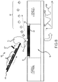
- FIG. 1 -A shows an embodiment of a molecular electronic sensing circuit, in which a molecule completes an electrical circuit, an electrical circuit parameter is measured versus time for signals, where the recorded signals correspond to interactions of the molecule with interacting molecules in the surrounding environment;
- FIG. 1 -B shows an embodiment of a processive enzyme molecular electronics sensor that can be used to read data encoded into synthetic DNA molecules.
- the sensor produces distinguishable signals corresponding to distinct signaling features structurally present on a template DNA molecule; such feature elements can be used to encode information into synthetic template DNA molecules, which can in turn be read via the sensor;
- FIG. 2 shows representative processive enzymes that can be used in a molecular sensor to act on various forms of DNA, including specific examples of a polymerase, a helicase, an exonuclease, and a DNA packaging molecular motor. Illustrated are: Klenow+DNA, Protein DataBase (PDB) structure ID 1KLN; Exonuclease I E Coli , PDB ID 1FXX; PDB ID 1G8Y; the crystal structure of the hexameric replicative helicase REPA; PDB ID 3EZK, Bacteriophage T4 gp17 motor assembly based on crystal structures and cryo-EM reconstructions; PDB ID 2WWY; and the structure of human RECQ-like helicase in complex with a DNA substrate;
- PDB Protein DataBase
- FIG. 2 shows representative processive enzymes that can be used in a molecular sensor to act on various forms of DNA, including specific examples of a polymerase, a helicase, an exonu
- FIG. 3 -A shows an embodiment of a processive enzyme molecular sensor in the process of reading DNA, in which groups bound to the template DNA are displaced by the action of the processive enzyme, with the displacement events resulting in distinguishable signal features;
- FIG. 3 -B shows an embodiment of a processive enzyme molecular sensor in the process of reading DNA, in which the template DNA has modifying groups attached, and as the processive enzyme translocates past these features, it results in the production of distinguishable signal features;
- FIG. 4 -A shows an embodiment of a processive enzyme molecular sensor comprising a processive enzyme molecule conjugated to a bridge molecule that spans the gap between two electrodes, conjugated to each electrode;
- FIG. 4 -B shows an embodiment of a processive enzyme molecular sensor comprising a processive enzyme molecule wired directly into the current path of the sensor by way of two arm molecules providing the connections to the electrodes;
- FIG. 4 -C shows an embodiment of a processive enzyme molecular sensor, wherein the processive enzyme molecule is directly conjugated to the electrodes without any intervening arm molecules or a bridge molecule in the circuit;
- FIG. 5 illustrates embodiments of a processive enzyme molecular sensor, wherein the processive enzyme comprises a polymerase having strand displacing activity
- FIG. 6 illustrates embodiments of a processive enzyme molecular sensor, wherein the processive enzyme comprises a helicase having strand displacing activity
- FIG. 7 illustrates embodiments of a processive enzyme molecular sensor, wherein the processive enzyme comprises a DNA packaging molecular motor having the ability to displace bound oligonucleotides sufficiently sterically bulky so as not to fit through the motor inlet;
- FIG. 8 illustrates embodiments of a processive enzyme molecular sensor, wherein the processive enzyme comprises an exonuclease having strand displacing activity
- FIG. 9 illustrates embodiments of a processive enzyme molecular sensor, wherein the processive enzyme comprises a helicase
- FIG. 10 illustrates embodiments of a processive enzyme molecular sensor, wherein the processive enzyme comprises a DNA packaging molecular motor;
- FIG. 11 illustrates embodiments of a processive enzyme molecular sensor, wherein the processive enzyme comprises an exonuclease
- FIG. 12 -A shows the detailed protein structure of one specific processive enzyme molecule, a polymerase comprising the Klenow Fragment of E. Coli . Polymerase I, with (A) and without (B) a DNA substrate interacting with the polymerase;
- FIG. 12 -B shows the detailed protein structure of one specific processive enzyme molecule, a helicase comprising the human RECQ-like DNA helicase while interacting with a DNA substrate molecule;
- FIG. 13 -A shows embodiments of a processive enzyme molecular electronic sensor, wherein the polymerase processive enzyme molecule is conjugated to a bridge molecule bonded between the electrodes;
- FIG. 13 -B shows an embodiment of the processive enzyme molecular electronic sensor of FIG. 13 -A, wherein the bridge molecule comprises a double stranded DNA, the polymerase-bridge conjugation comprises biotin-streptavidin binding, and the electrodes comprise gold-on-chromium to support thiol-gold binding of first and second ends of the bridge molecule to the electrodes;
- FIG. 13 -C shows embodiments of a processive enzyme molecular electronic sensor, wherein the polymerase processive enzyme is conjugated directly into the current path by use of two arm molecules between the enzyme and each of the two electrodes;
- FIG. 13 -D shows embodiments of a processive enzyme molecular electronic sensor, wherein the polymerase processive enzyme is conjugated directly into the current path, and directly to the metal electrodes, without use of arm or bridge molecules;
- FIG. 13 -E shows embodiments of a processive enzyme molecular electronic sensor, wherein the processive enzyme comprises a helicase (human RECQ-like helicase) and is conjugated to a bridge molecule that spans the gap between the spaced-apart electrodes;
- the processive enzyme comprises a helicase (human RECQ-like helicase) and is conjugated to a bridge molecule that spans the gap between the spaced-apart electrodes;
- FIG. 14 -A shows the physical structure of various embodiments of different DNA data encoding template molecules, wherein the signaling features are: (A) bound DNA oligonucleotides, (B) bound DNA oligonucleotides further comprising additional modifying groups, (C) single stranded DNA further comprising modifying groups, and (D) double stranded DNA further comprising modifying groups;
- FIG. 14 -B shows template structures (strand architectures) that allow a data payload from a single DNA molecule to be read multiple times by the same processive enzyme molecular sensor;
- FIG. 15 shows various embodiments of the logical structure for DNA data storage molecules, comprising handling adapters, a start site for the processive enzyme to engage, buffer segments, and a data payload segment encoding the primary binary data payload;
- FIG. 16 shows examples of Binary Data Encoding Schemes (“BES”) that can be used to encode digital information into the DNA data payload segment of a synthetic DNA molecule, for later reading by a processive enzyme molecular electronic sensor;
- BES Binary Data Encoding Schemes
- FIG. 17 -A shows an embodiment of a fabrication stack usable to put a plurality of DNA reader sensors on a chip for massively parallel, low-cost deployment of a DNA reading system
- FIG. 17 -B shows an embodiment of CMOS chip and pixel architecture for a chip-based array of processive enzyme molecular sensors.
- the sensor is formatted into scalable CMOS chip sensor array architecture, with molecular electronic sensor and source, gate and drain terminals;
- FIG. 18 shows an embodiment of a circuit schematic and the resulting measurement for the pixel circuit of FIG. 17 -B, comprising sensing of a 10 pA current, for one possible choice of circuit parameters (transistor properties, resistors and capacitors);
- FIG. 19 shows the completed, annotated chip design, and a drawing of an optical microscope image of the fabricated chip, for an embodiment of the pixel array chip of FIG. 17 -B having an array of 256 pixels;
- FIG. 20 shows a drawing of an electron microscope image of the fabricated chip of FIG. 19 , including insets of the nano-electrode with a polymerase processive enzyme molecular complex in place;
- FIG. 21 shows a schematic of a complete system for reading DNA data with chip-based DNA reader comprising processive enzyme molecular electronic sensors
- FIG. 22 shows a schematic of a cloud-based DNA data archival storage system, in which a multiplicity of the DNA reading system of FIG. 21 are aggregated to provide the data reader server;
- FIG. 23 shows an alternate embodiment of a DNA data reader sensor in which a processive enzyme is complexed with a different electronic sensor configuration than in FIG. 1 , here a nanopore ion current sensor, and which produces distinguishable signal features in the nanopore ion current when processing a DNA template molecule having signaling features;
- FIG. 24 shows an embodiment of DNA data reader sensor of FIG. 23 , in which the Helicase is directly conjugated to the nanopore, and in which the signaling groups are oligonucleotides bound to the DNA template, which further carry groups that alter the current in the nanopore sensor as they are translated past the pore by the action of the Helicase;
- FIG. 25 shows the concept of a DNA data reader sensor which a processive enzyme molecule is complexed with a carbon nanotube molecular wire spanning positive and negative electrodes, and produces distinguishable signal features in the measured current passing through the carbon nanotube;
- FIG. 26 shows an embodiment of a Zero Mode Waveguide sensor complexed with a processive enzyme molecule, shown in cross section, which produces distinguishable optical signals corresponding to DNA features, here due to dye molecules attached to oligonucleotides bound to the template DNA;
- FIG. 27 shows embodiments of a processive enzyme molecular electronic sensor, capable of reading information stored in a polymer other than DNA, comprising a lysozyme enzyme that produces distinguishable signals from signaling groups attached to a peptidoglycan polymer that is digested by the enzyme.
- a molecular electronics sensor comprising a processive enzyme that extracts information from DNA molecules by reading digital data stored as DNA.
- the present disclosure further provides a means of deploying such sensors in a chip-based format, and a resulting data reading system that supports such a chip-based sensor device.
- Reading information encoded into DNA molecules by use of the processive enzyme molecular sensors of the present disclosure is fundamental to overall methods and systems for DNA data storage.
- Various aspects of these methods and systems for DNA data storage including aspects of molecular sensors for reading DNA molecules encoded with digital information, is disclosed in PCT Application Serial No. PCT/US2018/013140, filed Jan. 10, 2018 and entitled “METHODS AND SYSTEMS FOR DNA DATA STORAGE,” the disclosure of which is incorporated herein by reference in its entirety for all purposes.
- DNA may refer not only to the biological DNA molecule, but also to fully synthetic versions, made by the methods of synthetic chemistry, such as nucleotide phosphoramidite chemistry, or by serial ligation of DNA oligomers, and also to forms made with chemical modifications present on the bases, sugar, or backbone, of which many are known to those skilled in nucleic acid biochemistry, including methylated bases, adenylated bases, other epigenetically marked bases, or also including non-standard or universal bases, such as inosine or 3-nitropyrrole, or other nucleotide analogues, or ribobases, or abasic sites, or damaged sites, and also including such DNA analogues as Peptide Nucleic Acids (PNA), Locked Nucleic Acids (LNA), Xeno Nucleic Acids (XNA) (a family of sugar-modified forms of DNA, including Hexitol Nucleic Acid (HNA)), Glycol Nucleic
- PNA Peptide Nu
- DNA in the context of referring to the data storage molecule used in a DNA storage system, including a template single strand, a single strand with oligomers bound thereon, double stranded DNA, and double strands with bound groups such as groups to modify various bases.
- DNA may refer to the single stranded forms of such molecules, as well as double helix or double-stranded forms, including hybrid duplex forms, including forms that containing mismatched or non-standard base pairings, or non-standard helical forms such as triplex forms, as well as molecules that are partially double stranded, such as a single-stranded DNA bound to an oligonucleotide primer, or a molecule with a hairpin secondary structure.
- DNA refers to a molecule comprising a single-stranded DNA component having bound oligonucleotide segments and/or perturbing groups that can act as the substrate for a processive enzyme to process, and in doing so, generate distinguishable signals in a monitored electrical parameter of a molecular sensor comprising the processive enzyme.
- GATTACA SEQ ID NO: 1
- GATTACA SEQ ID NO: 1
- SEQ ID NO: 1 represents the single stranded DNA molecule 5′-G-A-T-T-A-C-A-3′ (SEQ ID NO: 1).
- the convention used herein follows the standard convention for written DNA sequences used in the field of molecular biology.
- dNTP may refer not only to the standard, naturally occurring nucleoside triphosphates used in biosynthesis of DNA—i.e. dATP, dCTP, dGTP, and dTTP—but also to natural or synthetic analogues or modified forms of these, include those that carry base modifications, sugar modifications, or phosphate group modifications, such as an alpha-thiol modification or gamma phosphate modifications, or the tetra-, penta-, hexa- or longer phosphate chain forms, or possibly with additional groups conjugated to any of the phosphates, particularly the beta, gamma or higher order phosphates in the chain.
- dNTP may mean any nucleoside triphosphate analogue or modified form that can be incorporated by a polymerase enzyme as it extends a primer, or that would enter the active pocket of such an enzyme and engage transiently as a trial candidate for incorporation.
- oligonucleotide or “binding oligonucleotide” refers to a short segment of DNA, or analog forms described above, having a length in the range of 3-100 bases, or 5-40 bases, or 10-30 bases, which can hybridize with complementary sequence contain in a template strand. Such hybridization may be through perfect Watson-Crock base-paring matches, or may involve mismatches or nonstandard base pairings.
- hybridization refers to the process of complementary strand binding as it occurs in the DNA double helix, or in similar duplex formation for DNA analogs.
- buffer refers to a solution which provides the environment in which the processive enzyme sensor can operate and produce signals from supplied DNA templates.
- the solution is an aqueous solution, which may comprise dissolved, suspended or emulsified components such as salts, pH buffers, divalent cations, surfactants, blocking agents, solvents, template primer oligonucleotides, other proteins that complex with the polymerase, and also possibly including the polymerase substrates, i.e. dNTPs, analogues or modified forms of dNTPs, and DNA molecule substrates or templates.
- binary data or “digital data” refers to data encoded using the standard binary code, or a base 2 ⁇ 0,1 ⁇ alphabet, data encoded using a hexadecimal base 16 alphabet, data encoded using the base 10 ⁇ 0-9 ⁇ alphabet, data encoded using ASCII characters, or data encoded using any other discrete alphabet of symbols or characters in a linear encoding fashion.
- digital data encoded format refers to the series of binary digits, or other symbolic digits or characters that come from the primary translation of the DNA sequence features used to encode information in DNA, or the equivalent logical string of such classified DNA features.
- information to be archived as DNA may be translated into binary, or exist initially as binary data, and then this data may be further encoded with error correction and assembly information, into the format that is directly translated into the code provided by the distinguishable DNA signaling features. This latter association is the primary encoding format of the information.
- Application of the assembly and error correction procedures is a further, secondary level of decoding, back towards recovering the source information.
- the term “signaling feature” refers to a characteristic of a data-encoding DNA molecule that, when encountered and processed by the processive enzyme of a processive enzyme molecular sensor, produces a signal in a monitored electrical parameter of the sensor circuit, such as current (i).
- Arrangements of signaling features on a DNA molecule are used to encode information in a synthetic DNA molecule.
- the broader group of signaling features herein further comprise both “bound groups” capable of displacement by a processive enzyme of a sensor and “perturbing groups” that are not displaced from the DNA molecule by the processive enzyme. Both types of signaling features on a DNA molecule provide distinct signals in a monitored electrical parameter of the sensor circuit when encountered by the processive enzyme of the sensor.
- Signaling features comprise, for example, hybridization-bound oligonucleotides, chemical groups conjugated to the DNA, or combinations of such to achieve arrangements of features that produce distinguishable signals when processed by the sensor processive enzyme.
- DNA data encoding molecule refers to a DNA molecule synthesized to encode data, such as binary information, in its molecular structure, including copies of information containing DNA molecules or other DNA molecules derived from such molecules, such as complementary sequences.
- reading data from DNA refers to any method of measuring distinguishable events, such as electrical signals or other perturbations in a monitored electrical parameter of a circuit, which correspond to molecular features in a synthetic DNA molecule that were used to encode information into the DNA molecule.
- electrodes refer to nano-scale electrical conductors (more simply, “nano-electrodes”), disposed in pairs and spaced apart by a nanoscale-sized electrode gap between the two electrodes in any pair of electrodes.
- the term “electrode” may refer to a source, drain or gate.
- a gate electrode may be capacitively coupled to the gap region, and may be a “buried gate,” “back gate,” or “side gate.”
- the electrodes in a pair of spaced-apart electrodes may be referred to specifically (and labeled as such in various drawing figures) as the “source” and “drain” electrodes, “positive” and “negative” electrodes, or “first” and “second” electrodes.
- Nano-scale electrodes in a pair of electrodes are spaced apart by an electrode gap measuring about 1 nm to 100 nm, and may have other critical dimensions, such as their width, height, and length, also in this same nanoscale range.
- Such nano-electrodes may be composed of a variety of materials that provide conductivity and mechanical stability. They may be comprised of metals, or semiconductors, for example, or of a combination of such materials. Pairs of spaced-apart electrodes may be disposed on a substrate by nano-scale lithographic techniques.
- enzyme refers to any molecule or molecular complex that acts on a substrate molecule to alter its state. Such enzymes are often proteins or comprise a protein component.
- a “processive enzyme” refers to any enzyme having “processivity,” which is the ability to catalyze consecutive reactions without the enzyme releasing its substrate.
- a processive enzyme may process a DNA molecule by engaging the DNA molecule at one end of the molecule or at an internal initiation site and translocating along the DNA molecule. This translocative movement is, of course, relative, and it may be the substrate that moves through a processive enzyme if the enzyme is physically anchored in a molecular sensor.
- Processive enzymes include, but are not limited to, polymerases, helicases, exonucleases, and molecular motors for packaging virus DNA.
- a “bridge molecule” refers to a molecule bound between two spaced-apart electrodes in a pair of electrodes, to span the electrode gap there between, and complete an electrical circuit.
- a bridge molecule has roughly the same length as an electrode gap, such as 1 nm to 100 nm, or in some cases, about 10 nm.
- Bridge molecules for use herein may comprise double stranded DNA, other analog DNA duplex structures, such as DNA-RNA, DNA-PNA or DNA-LNA or DNA-XNA duplex hybrids, peptides, protein alpha-helix structures, antibodies or antibody Fab domains, graphene nanoribbons or carbon nanotubes, silicon nanowires, or any other of a wide array of molecular wires or conducting molecules known to those skilled in the art of molecular electronics.
- a bridge molecule herein may be described as having a “first” and “second” end, such as a base at or near the 3′ end and a base at or near the 5′ end of a DNA molecule acting as a bridge molecule.
- each end may be chemically modified such that the first end of a bridge molecule bonds to a first electrode and the second end of a bridge molecule bonds to a second electrode in a pair of spaced-apart electrodes.
- This nomenclature aids in visualizing a bridge molecule spanning an electrode gap and bonding to each electrode in a pair of spaced-apart electrodes.
- the first and second ends of a bridge molecule may be chemically modified so as to provide for self-assembly between the bridge molecule and a processive enzyme and/or between the bridge molecule and one or both electrodes in a pair of electrodes.
- an “arm” molecule has many of the same characteristics as a bridge molecule, and may comprise the same chemical species, e.g., DNA, although an arm molecule may be of shorter molecular length so that it may assist bonding a processive enzyme to only one electrode in a pair of spaced-apart electrodes.
- at least two arm molecules may be used to electrically connect a processive enzyme to both electrodes in a pair of spaced-apart electrodes, thereby suspending it between electrodes without directly bonding the enzyme to either electrode.
- conjugation refers to a chemical linkage, (i.e., bond), of any type known in the chemical arts, e.g., covalent, ionic, Van der Waals, etc.
- the conjugations of a processive enzyme to bridge and/or arm molecules, or conjugations between bridge or arm molecules to an electrode may be accomplished by a diverse array of conjugation methods known to those skilled in the art of conjugation chemistry, such as biotin-avidin couplings, thiol-gold couplings, cysteine-maleimide couplings, gold binding peptides or material binding peptides, click chemistry coupling, Spy-SpyCatcher protein interaction coupling, or antibody-antigen binding (such as the FLAG peptide tag/anti-FLAG antibody system), and the like.
- Conjugation of a processive enzyme to each electrode in a pair of spaced-apart electrodes comprises an “electrical connection” or the “electrical wiring” of the enzyme into a circuit that includes the enzyme and the pair of electrodes.
- the enzyme is conjugated to each electrode in a pair of electrodes to provide a conductive pathway between the electrodes that would be otherwise be insulated from one another by the electrode gap separating them.
- a conductive pathway is provided by electron delocalization/movement through the chemical bonds of the enzyme, such as through C—C bonds.
- FIG. 1 -A shows an embodiment of a molecular electronic sensing circuit in which a molecule completes an electrical circuit and an electrical circuit parameter is measured versus time to provide a signal, wherein variations in signal reflect interactions of the molecule with other molecules in the environment.
- a molecular electronics sensor 1 comprises a circuit in which a single sensor molecule 2 , (or alternatively, a sensor complex comprising a small number of molecules), forms a completed electrical circuit by spanning the electrode gap 9 between a pair of spaced-apart nano-scale electrodes 3 and 4 , comprising for example positive and negative electrodes, respectively, disposed on a support layer 5 .
- the sensor molecule may be electrically conjugated in place to each of the electrodes by specific attachment points 6 and 7 .
- an electronic parameter 100 of the circuit is measured as the sensor molecule 2 interacts with various interacting molecules 8 to provide signals 101 in the measured electronic parameter.
- the measured parameter 100 may comprise current (i) passing between the electrodes and through the sensor molecule 2 versus time, with the electrical signals 101 in the measured parameter indicative of molecular interactions between the interacting molecules 8 and the sensor molecule 2 , as illustrated by the plot of (i) versus (t) in FIG. 1 -A.
- a processive enzyme molecular electronics sensor 10 provides a reader for reading digital data encoded into a DNA molecule 18 .
- a molecular complex 12 comprises a molecular bridge 13 and a processive enzyme 14 bonded thereto for reading the digital data.
- the single enzyme molecule 14 processively engages with a target DNA molecule 18 , translocating along the DNA as it acts on it, and by doing so produces electrical signals 102 in the measured electronic parameter of the circuit as it processes along the DNA template, as shown in the plot of (i) versus (t) at the left of the figure.
- the DNA template molecule 18 is augmented with “signaling features” 17 , each of which results in a distinguishable electrical signal 102 in the (i) versus (t) plot when the processive enzyme 14 encounters the signaling feature.
- the processive enzyme sensor 10 produces a series of distinguishable electrical signals (e.g., 103 and 104 shown in the inset plot of (i) versus (t)), corresponding to the specific distinct signaling features 17 provided in predetermine patterns on the template DNA molecule 18 .
- the inset in FIG. 1 -B shows the alignment between the signaling features on the DNA molecule (indicated as “Feat. 1 ” and “Feat.
- distinguishable signal features 17 can therefore encode information in a synthetic DNA molecule, and may be incorporated into DNA through a variety of encoding schemes, (e.g., discussed below in reference to FIG. 16 ).
- the processive enzyme is a critical element within a processive enzyme molecular sensor that is capable of reading DNA molecules.
- processive enzymes capable of processively engaging with DNA, such as to perform various biological functions in various organisms.
- the important feature here is that the enzyme translocates along the DNA molecule in the course of its function.
- Such enzymes typically have a specific recognition structure that may occur at one end of a DNA strand, and they engage at that site, and initiate a process in which they translocate along the DNA molecule in one direction, perhaps performing some further function as they move along the molecule.
- Such translocation can in some cases be entirely unidirectional or can in other cases be predominantly in one direction, but with the possibility of reverse motions.
- Such translocation may process the entire DNA molecule from one end to the other, or may halt or disengage before reaching the other end.
- FIG. 2 illustrates non-limiting representatives of some major categories of processive enzymes that act on DNA templates. Shown from left to right are examples of a polymerase 21 , an exonuclease 22 , a helicase 23 , a molecular motor 24 for packaging DNA, and another helicase 25 . Each of these types of processive enzymes find use in a processive enzyme molecular sensor herein, and each perform a different major function in regards to processing DNA.
- the polymerase 21 illustrated in FIG. 2 is the E. Coli Klenow fragment polymerase (shown is structure 1KLN of the Protein Database (PDB)).
- a polymerase synthesizes a complementary strand as it translates along single-stranded template DNA.
- polymerases having strand-displacing activity meaning that, as they translocate along single-stranded DNA they displace the complementary strand to expose the template for the strand being synthesized if they encounter a double stranded segment.
- the exonuclease 22 illustrated in FIG. 2 is the E. Coli exonuclease I (PDB structure 1FXX).
- an exonuclease digests a DNA strand as it translocates along it, one base at a time, starting from one end.
- Various forms act on single or double stranded DNA, and may digest one or both strands.
- Exonucleases may have a chemical polarity in the direction they digest the strand (i.e., 3′ to 5′ or 5′ to 3′), and may require different types of initiation. Exonucleases may behave in different ways when they encounter various alterations in the strands they are processing, such as a change between single and double stranded forms, or the presence of chemically modified bases, or adducts, or attached groups.
- helicase 23 is the bacterial Helicase REPA, (PDB ID 1G8Y), which is a hexameric protein complex.
- the helicase 25 illustrated in FIG. 2 is the human RECQ-like DNA helicase.
- a helicase unzips the complementary strands as it translocates along double stranded DNA.
- Various types of helicases may also purely translocate along single-stranded DNA, performing no other activity.
- the packaging motor protein 24 illustrated in FIG. 2 is the motor protein gp17 from the T4 bacteriophage (PDB ID 3EZK).
- a DNA packaging motor translocates a DNA strand into the capsule of a viral particle as part of the process of viral replication. Such motors may translocate along a single or double stranded DNA molecule.
- FIG. 2 illustrates only non-limiting examples of enzymes that processively engage with DNA. There are many other specific proteins from these categories, as well as other forms of processive enzymes well known to those in the field of molecular biology that find use in the processive enzyme molecular sensors of the present disclosure. Further, the enzymes illustrated in FIG. 2 comprise the native forms of these enzymes. It is understood that for the processive enzyme molecular sensors of the present disclosure, native enzymes may be used, or enzymes that have been genetically modified to provide conjugation groups at specific sites, such as to modify or augment their activity, rate of translocation, or tolerance for modifications on a DNA molecule.
- FIG. 3 -A illustrates various embodiments of a processive enzyme molecular electronics sensor 30 capable of reading digital information encoded and stored in DNA.
- the processive enzyme molecular sensor 30 comprises a molecular sensor complex 32 spanning electrode gap 39 and further comprising a bridge molecule 33 and a processive enzyme 34 bound thereto.
- the DNA template molecule 38 comprises bound groups 37 , capable of displacement from the DNA as the processive enzyme 34 translocates along the DNA molecule 38 .
- a displacement event comprising displacement of a bound group 37 from the DNA molecule 38 to an unbound group 37 ′, generates a corresponding signal feature in a monitored electrical parameter such as current (i) through the sensor circuit versus time (t).
- a monitored electrical parameter such as current (i) through the sensor circuit versus time (t).
- the displacement events may appear as peaks 301 , 302 , 303 and so forth, or other distinguishable electrical signals, corresponding to each of the displacement events, in the (i) versus (t) plot.
- bound groups 37 comprise encoded digital information, encoded in DNA molecules such as, for example, by the encoding schemes of FIG. 16 .
- bound groups 37 may comprise DNA oligonucleotides hybridized to single stranded DNA, or oligonucleotides further comprising a signal enhancing modification such as an attached charged group or structural group. Such constructs are illustrated in the upper two structures of FIG. 14 , discussed herein.
- FIG. 3 -B illustrates another series of embodiments of a processive enzyme molecular electronics sensor 31 for reading digital information stored in DNA.
- the molecular sensors 31 comprise a molecular sensor complex 312 spanning the electrode gap 319 and further comprising a bridge molecule 313 and a processive enzyme 314 bonded thereto.
- a DNA template molecule 318 further comprises perturbing groups 317 integrated into the molecule, wherein such groups 317 remain on the DNA template molecule as the DNA molecule translocates through the processive enzyme 314 , and where in so doing the local perturbations present in the molecule result in distinguishable perturbation signals 304 , 305 , and 306 in the monitored electrical parameter, such as (i) versus (t).
- perturbing groups 317 may comprise modifications to the bases of the DNA, including modification to the nucleobase, the sugar residue, or the phosphate backbone. A very large number of such base modifications are well known to those in the field of molecular biology. Modifications may further comprise groups conjugated to modified bases, such as by any standard means of conjugation, including click chemistry coupling, biotin-based coupling, N-hydroxysuccinimide (NHS) conjugation, maleimide conjugation, or any of many other methods known for conjugating groups to DNA.
- the processive enzyme molecular sensor embodiments illustrated in FIGS. 3 -A and 3 -B comprise a molecular complex.
- the molecular complex is illustrated generically as comprising a bridge molecule (oval shape) and a processive enzyme (globular shape) bonded thereto.
- the molecular complex is electrically connected between a pair of spaced-apart electrodes to span the electrode gap and complete an electronic circuit.
- the processive enzyme may be integrated as part of the molecular complex in various ways.
- FIGS. 4 -A, 4 -B, and 4 -C illustrate various non-limiting embodiments for this complex and how the enzyme is integrated into an electronic circuit that comprises the molecular complex.
- FIG. 4 -A shows an embodiment of a processive enzyme molecular sensor 40 in which the processive enzyme 44 is conjugated, via a one or more conjugations points 46 , to a bridge molecule 43 that spans the electrode gap 49 .
- the bridge molecule 43 comprises first and second ends capable of attachment to each of the electrodes at attachment points 47 and 48 .
- the bridge molecule is electrically connected to each electrode in a pair of spaced-apart electrodes, such as the positive and negative electrodes shown, to span the electrode gap 49 between electrodes and complete the sensor circuit.
- FIG. 4 -B shows an embodiment of a processive enzyme molecular sensor 410 in which the processive enzyme 412 is conjugated directly into the current path between the electrodes, spanning the electrode gap 419 , by conjugation to two separate “arm” molecules 413 and 414 , which in turn are conjugated at one of their ends to each of the two electrodes via attachment points 416 and 417 , and to bonding sites on the enzyme 412 at conjugation points 415 and 418 , as shown.
- FIG. 4 -C shows an embodiment of a processive enzyme molecular sensor 420 in which the processive enzyme 422 is conjugated directly to the electrodes to span the electrode gap 430 via the conjugation points 428 and 425 , without any intervening arm or bridge molecules to assist in conjugating the enzyme to the electrodes. In this way, the processive enzyme 422 is directly wired into and functions as an element of the sensor circuit.
- the enzyme may be a native or mutant form of a polymerase, a reverse transcriptase, a helicase, an exonuclease, or a molecular motor for packaging DNA into a virus.
- the mutated enzyme forms enable site specific conjugation of the enzyme to a bridge molecule, to one or more arm molecules, or to each of the electrodes in a pair of spaced-apart electrodes, through introduction of specific conjugation sites in the enzyme.
- Such conjugation sites engineered into the protein by recombinant methods or methods of synthetic biology may in various embodiments comprise any one of a cysteine, an aldehyde tag site (e.g. the peptide motif CxPxR), a tetracysteine motif (e.g. the peptide motif CCPGCC (SEQ ID NO: 2)), and an unnatural or non-standard amino acid (NSAA) site, such as through the use of an expanded genetic code to introduce a p-acetylphenylalanine, or an unnatural crosslinkable amino acid, such as through the use of RNA- or DNA-protein cross-link using 5-bromouridine, (see Gott, J. M., et al., Biochemistry, 30 (25), 6290-6295 (1991)).
- an aldehyde tag site e.g. the peptide motif CxPxR
- a tetracysteine motif e.g. the peptide motif CCPGCC (SEQ ID
- the bridge molecules or arm molecules may comprise double stranded DNA, other analog DNA duplex structures, such as DNA-RNA, DNA-PNA or DNA-LNA or DNA-XNA duplex hybrids, peptides, protein alpha-helix structures, antibodies or antibody Fab domains, graphene nanoribbons or carbon nanotubes, silicon nanowires, or any other of a wide array of molecular wires or conducting molecules known to those skilled in the art of molecular electronics.
- DNA-RNA DNA-PNA or DNA-LNA or DNA-XNA duplex hybrids
- peptides protein alpha-helix structures
- antibodies or antibody Fab domains graphene nanoribbons or carbon nanotubes
- silicon nanowires or any other of a wide array of molecular wires or conducting molecules known to those skilled in the art of molecular electronics.
- conjugation of a processive enzyme to such molecules, or of such molecules to the electrodes may be accomplished by a diverse array of conjugation methods known to those skilled in the art of conjugation chemistry, such as biotin-avidin couplings, thiol-gold couplings, cysteine-maleimide couplings, gold binding peptides or material binding peptides, click chemistry coupling, Spy-SpyCatcher protein interaction coupling, or antibody-antigen binding (such as the FLAG peptide tag/anti-FLAG antibody system) etc.
- conjugation chemistry such as biotin-avidin couplings, thiol-gold couplings, cysteine-maleimide couplings, gold binding peptides or material binding peptides, click chemistry coupling, Spy-SpyCatcher protein interaction coupling, or antibody-antigen binding (such as the FLAG peptide tag/anti-FLAG antibody system) etc.
- Coupling of molecules to electrodes may be done via material binding peptides, or through the use of a SAM (Self-Assembling-Monolayer) or other surface derivatization on the electrode surface to present suitable functional groups for conjugation, such as azide or amine groups.
- the electrodes herein comprise electrically conducting nanoscale-dimensioned structures, which may comprise a metal, such as gold, silver, platinum, palladium, aluminum, chromium, or titanium, layers of such metals, such as gold on chromium, or semiconductors, such as doped silicon, or doped germanium.
- a contact point of a first material may be disposed on a supporting second material, such that the contact point is a site that directs chemical self-assembly of the molecular complex to the electrode.
- a sensor may comprise spaced-apart pairs of titanium or platinum electrodes having a gold dot contact point deposited on each one of the electrodes to direct self-assembly of bridge molecules to the contact points such that only one bridge molecule spans each electrode gap between a pair of spaced-apart electrodes.
- FIG. 5 shows embodiments of a processive enzyme molecular sensor 50 wherein the processive enzyme comprises a polymerase 54 having strand displacing activity.
- sensor 50 comprises processive enzyme 54 conjugated at one or more attachment points 55 to a bridge molecule 53 bonded between electrode pairs and spanning the electrode gap 59 .
- the bridge molecule 53 comprises first and second ends functionalized to bond to the electrode pair at conjugation points 51 and 52 .
- the processive translocation occurs as the polymerase 54 extends the 3′ end of the primed strand 58 , and synthesizes the complementary strand 58 ′ of the underlying template strata. This takes place in a suitable buffer that also supplies dNTPs 56 for the synthesis of the complementary strand, as indicated.
- the signaling features 57 are DNA oligonucleotides hybridized to the template strand 58 .
- the strand displacing polymerase 54 will displace and remove these oligonucleotides (as exemplified by the displacement of oligonucleotide 57 ′) as it translocates in the course of synthesis.
- Each strand displacement event may generate a signal in the measured current of the circuit, as indicated by perturbations 501 , 502 and 503 in the (i) versus (t) plot.
- the hybridizing oligonucleotides 57 may be DNA or DNA analogs, and may have further groups attached to enhance signaling, such as described further below in the context of FIG. 14 .
- FIG. 6 shows further embodiments of a processive enzyme molecular sensor 60 wherein the processive enzyme 64 comprises a helicase also having strand displacing activity.
- sensor 60 comprises processive enzyme 64 conjugated at one or more attachment points 65 to a bridge molecule 63 bonded between electrode pairs and spanning the electrode gap 69 .
- the bridge molecule 63 comprises first and second ends functionalized to bond to the electrode pair at conjugation points 61 and 62 .
- the signaling features 67 are DNA oligonucleotides hybridized to the template strand 68 .
- the strand displacing helicase 64 will displace and remove these oligonucleotides (such as illustrated by displacement of oligonucleotide 67 ′) as it translocates.
- Each strand displacement event may generate a signal in the measured current of the circuit, as indicated by the perturbations 601 , 602 , and 603 in the (i) versus (t) plot.
- the hybridizing oligonucleotides 67 in question comprise DNA or DNA analogs, and may have further groups attached to enhance signaling, such as described further below in the context of FIG. 14 .
- FIG. 7 shows further embodiments of a processive enzyme molecular sensor 70 wherein the processive enzyme 74 comprises a DNA packaging molecular motor also having the ability to displace a bound oligonucleotide 77 ′ that is sufficiently sterically bulky to not fit through the motor inlet.
- sensor 70 comprises processive enzyme 74 conjugated at one or more attachment points 75 to a bridge molecule 73 bonded between electrode pairs and spanning the electrode gap 79 .
- the bridge molecule 73 comprises first and second ends functionalized to bond to the electrode pair at conjugation points 71 and 72 .
- the signaling features comprise DNA oligonucleotides 77 hybridized to the template strand 78 .
- the strand displacing motor 74 will displace and remove these oligonucleotides (such as 74 ′ thus displaced) as it translocates the DNA.
- Each strand displacement event may generate a signal in the measured current of the circuit, as indicated by perturbations 701 , 702 , and 703 in the (i) versus (t) plot.
- the hybridizing oligonucleotides 77 in question may comprise DNA or DNA analogs, and may have further groups attached to enhance signaling, such as described further below in the context of FIG. 14 .
- the oligonucleotides 77 may include a sterically hindering group that makes them too large to fit through the motor inlet, such as a polyethylene glycol (PEG) group, an Avidin protein group, or any other bulky group that can be readily attached to a DNA oligonucleotide.
- a sterically hindering group that makes them too large to fit through the motor inlet
- PEG polyethylene glycol
- Avidin protein group an Avidin protein group
- Many such groups are known and readily available to those skilled in molecular biology.
- FIG. 8 shows embodiments of a processive enzyme molecular sensor wherein the processive enzyme 84 comprises an exonuclease also having strand displacing activity.
- sensor 80 comprises processive enzyme 84 conjugated at one or more attachment points 85 to a bridge molecule 83 bonded between electrode pairs and spanning the electrode gap 89 .
- the bridge molecule 83 comprises first and second ends functionalized to bond to the electrode pair at conjugation points 81 and 82 .
- the signaling features comprise DNA oligonucleotides 87 hybridized to the template strand 88 .
- the strand displacing exonuclease 84 will displace and remove these oligonucleotides (such as illustrated by the displacement of 87 ′) as it translocates and digests the primary strand 88 .
- Each strand displacement event may generate a signal in the measured current of the circuit, as indicated by the perturbations 801 , 802 , and 803 in the (i) versus (t) plot.
- the hybridizing oligonucleotides 87 may comprise DNA or DNA analogs, and may further comprise groups attached to enhance signaling, such as described further below in the context of FIG. 14 .
- some exonucleases may displace oligonucleotides 87 from the primary strand 88 by digesting entirely through the double stranded region of the paired segment, or by digesting only partially through it, at which point the remainder of the oligonucleotide dissociates from the primary strand.
- FIG. 9 shows embodiments of a processive enzyme molecular sensor 90 wherein the processive enzyme 94 comprises a helicase.
- sensor 90 comprises processive enzyme 94 conjugated at one or more attachment points 95 to a bridge molecule 93 bonded between electrode pairs and spanning the electrode gap 99 .
- the bridge molecule 93 comprises first and second ends functionalized to bond to the electrode pair at conjugation points 91 and 92 .
- the signaling features 96 , 97 are perturbing groups on the DNA strand 98 . As each perturbing group 96 , 97 passes by the helicase, it generates a signal in the measured current of the circuit, as indicated by 901 , 902 and 903 in the (i) versus (t) plot.
- the various perturbing groups 96 , 97 may be arranged in patterns that encode information.
- the illustration of this particular sequence of 96, 97, 97, 96, 96, and so forth is not intended to be limiting, and any number of different perturbing groups arranged in any pattern may be used in order to encode information.
- the DNA molecule may be single stranded, with the perturbing groups 96 , 97 on the single strand, and the helicase 94 may be purely translating along the single strand.
- the DNA may be double stranded, and the perturbing groups may be positioned on either strand, the one that goes “through” the helicase, to which it is bound, or the one that is displaced “around” the helicase.
- such perturbing groups may be positioned on both strands within the same double stranded DNA molecule. Such groups are described further below in the context of FIG. 14 .
- FIG. 10 shows embodiments of a processive enzyme molecular sensor 120 wherein the processive enzyme 124 comprises a DNA packaging motor.
- sensor 120 comprises processive enzyme 124 conjugated at one or more attachment points 125 to a bridge molecule 123 bonded between electrode pairs and spanning the electrode gap 129 .
- the bridge molecule 123 comprises first and second ends functionalized to bond to the electrode pair at conjugation points 121 and 122 .
- the signaling features 126 , 127 are perturbing groups on the DNA strand 128 .
- each perturbing group 126 , 127 passes by the motor 124 , it generates a corresponding signal in a monitored electrical parameter of the circuit, such as indicated by the changes 105 , 106 , and 107 seen in the (i) versus (t) plot.
- the various perturbing groups 126 , 127 may be arranged in patterns that encode information. The illustration of this particular sequence of 126 , 127 , 127 , 126 , 126 , and so forth is not intended to be limiting, and any number of different perturbing groups arranged in any pattern may be used in order to encode information.
- the DNA molecule may be single stranded, with the perturbing groups on the single strand, such as for a motor that translates a single strand. In other embodiments, the DNA may be double stranded, and the perturbing groups may be positioned on either strand, in the case of a motor that translocates double stranded DNA. Such groups are described further in the context of FIG. 14 .
- FIG. 11 shows embodiments of processive enzyme molecular sensors 110 wherein the processive enzyme 114 comprises an exonuclease.
- sensor 110 comprises processive enzyme 114 conjugated at one or more attachment points 115 to a bridge molecule 113 bonded between electrode pairs and spanning the electrode gap 119 .
- the bridge molecule 113 comprises first and second ends functionalized to bond to the electrode pair at conjugation points 111 and 112 .
- the signaling features 117 are perturbing groups on the DNA strand 118 .
- each perturbing group 117 As each perturbing group 117 passes near the exonuclease, it generates a signal in a monitored electrical parameter of the circuit, such as indicated by the perturbations 108 , 108 ′, and 108 ′′ in the (i) versus (t) plot.
- the action of the exonuclease 114 on the functionalized DNA 118 produces digestion products 116 as the DNA is digested by the enzyme.
- the digestion products comprise a mixture of bases and functionalized bases that retain a perturbation group, as shown.
- the illustration of this particular sequence of perturbing groups 117 is not intended to be limiting, and any number of different perturbing groups arranged in any pattern may be used in order to encode information.
- the DNA molecule 118 may be single stranded, with the perturbing groups 117 positioned on the single strand, for an exonuclease that digests a single strand, or the DNA may be double stranded, for an exonuclease that processes double stranded DNA, and the perturbing groups may be on either strand, and in the case where only one strand of a double stranded DNA is digested, the perturbing groups 117 may reside on the digested or on the non-digested strand, or both. Such groups are described further below in the context of FIG. 14 .
- FIG. 12 -A shows the detailed protein anatomy and DNA engagement of one of the exemplary processive enzymes for use herein, in this case a polymerase, and specifically the E. Coli Klenow fragment.
- the structure shown is PDB ID 1KLN.
- the detailed structure and how it engages the template DNA inform the choice of how to best conjugate the enzyme into the circuit, so as not to interfere with its interaction with DNA, and to position the signaling portions of the protein or DNA near to the molecular bridge for enhanced signal generation via proximity.
- the structure A at left is the polymerase engaged with a DNA substrate molecule whereas the structure B at right is the polymerase in its conformation absent engagement with a DNA substrate.
- the helix, sheet and loop portions of the enzyme are pointed out in both the engaged conformation and the conformation absent DNA engagement.
- FIG. 12 -B shows the detailed protein anatomy and DNA engagement of one of the exemplary processive enzymes for use herein, in this case a helicase, and specifically the human RECQ-like helicase.
- the structure shown is PDB ID 2WWY.
- the detailed structure and how it engages the template DNA inform the choice of how to best conjugate the enzyme into the circuit, so as not to interfere with its interaction with DNA, and to position the signaling portions of the protein or DNA near to the molecular bridge for enhanced signal generation via proximity.
- the structure shows the helicase engaged with a DNA substrate molecule. The helix, sheet and loop portions of the helicase are pointed out in the illustrated structure.
- FIG. 13 -A shows embodiments of a processive enzyme molecular sensor 130 A wherein the polymerase enzyme 134 A is conjugated to a molecular bridge molecule 133 A, at a conjugation point 135 A comprising a specific site on the enzyme 134 A bonded to a specific site on the bridge molecule 133 A.
- the bridge molecule 133 A is bonded to each of the spaced-apart electrodes to span the electrode gap 139 A.
- the bridge molecule 133 A comprises first and second ends functionalized to bond to the electrode pair at conjugation points 131 A and 132 A.
- the sensor 130 B further comprises a pair of spaced apart chromium electrodes 138 B and 139 B, disposed on a substrate layer, such as SiO 2 , and spaced apart at about 10 nm. On each electrode 138 B and 139 B are deposits of gold 131 B that participate in the bonding of the bridge molecule to each of the electrodes.
- the DNA bridge molecule 133 B shown is conjugated to the gold-on-chromium electrodes through thiol groups on first and second ends of the DNA bridge, binding to gold via sulfur-gold bonds 132 B, and wherein the polymerase 134 B is conjugated to the DNA bridge molecule 133 B at a centrally located biotinylated base on the DNA bridge 135 B, bound to a streptavidin molecule 136 B, in turn bound to the polymerase 134 B via a specific biotinylated site 135 B on the polymerase 134 B.
- the streptavidin 136 B links the polymerase 134 B to the DNA bridge molecule 133 B by way of two biotin-streptavidin linkages 135 B.
- the processive enzyme molecular sensor 130 B is illustrated translocating a DNA substrate molecule 137 B.
- the DNA substrate molecule 137 B may be encoded with information comprising arrangements of signaling features such as bound DNA oligonucleotide segments or perturbing groups.
- FIG. 13 -C shows embodiments of a processive enzyme molecular sensor 130 C wherein the polymerase molecule 134 C (also shown in FIG. 12 -A) is conjugated directly into the current path between the electrodes, spanning the electrode gap 139 C, by conjugation to two separate “arm” molecules 133 C and 134 C, which in turn are conjugated at one of their ends to each of the two electrodes via attachment points 136 C and 137 C, and to bonding sites on the enzyme 132 C at conjugation points 135 C and 138 C, as shown.
- the polymerase molecule 134 C also shown in FIG. 12 -A
- conjugations of the arm molecules may be to the ends of an alpha-helix spanning the enzyme, to loop or sheet portions, or to other such protein anatomical structures (e.g., pointed out in FIG. 12 -A) that preferentially channel the current through or near the active site of the enzyme or through or near portions of the enzyme that experience changes in conformation when interacting with a substrate molecule such as DNA molecule 131 C shown.
- a substrate molecule such as DNA molecule 131 C shown.
- FIG. 13 -D shows embodiments of a processive enzyme molecular sensor 130 D wherein the polymerase molecule 132 D (also shown in FIG. 12 -A) is conjugated directly to the each of the electrodes in a pair of spaced-apart electrodes to span the electrode gap 139 D without any intervening arm or bridge molecules, in accordance with the general sensor structure of FIG. 4 -C.
- the polymerase 132 D is conjugated directly to the electrodes at attachment points 136 D and 137 D, wherein the attachment points may comprise thiol-gold bonds.
- These embodiments illustrate how the conjugations may be to the ends of an alpha-helix spanning the enzyme, to loop or sheet portions, or to other such protein anatomical structures (e.g., pointed out in FIG. 12 -A) that preferentially channel the current through or near the active site of the enzyme or through or near portions of the enzyme that experience changes in conformation when interacting with a substrate molecule such as DNA molecule 131 D shown.
- FIG. 13 -E shows embodiments of a processive enzyme molecular sensor 130 E wherein the helicase enzyme molecule 132 E (also shown in FIG. 12 -B) is conjugated to a molecular bridge molecule 133 E, at a specific conjugation point 135 E comprising a specific binding site on both the helicase and the bridge molecule, in accordance to the general sensor structure shown in FIG. 4 -A.
- the bridge molecule 133 E comprises first and second ends, each bonded to the pair of electrodes at attachment points 136 E and 137 E.
- the conjugation point 135 E between the helicase 132 E and the bridge molecule 133 E is chosen to bring the most active or variable parts of the helicase 132 E, or the signaling groups bonded on the DNA substrate molecule 131 E to be processively processed by the helicase 132 E, in close proximity to the bridge molecule 133 E for enhanced current modulation and enhanced signaling.
- the electrical parameter measured in the processive enzyme molecular sensors described herein for distinguishable signals can in general be any electrical property of the circuit measurable while the sensor is active.
- the parameter is the current passing between the two electrodes in a pair of spaced-apart and bridged electrodes versus time, either continuously or sampled at discrete times, when a voltage, fixed or varying, is applied between the electrodes.
- the measured parameter may be the resistance, conductance, or impedance between the two electrodes, measured continuously versus time or sampled periodically.
- the measured parameter could be the voltage between the electrodes. If there is a gate electrode, the measured parameter could be the gate voltage. The measured parameter could also be a capacitance, or the amount of charge or voltage accumulated on a capacitor coupled to the circuit.
- the measurement could be a voltage spectroscopy measurement, such that the measurement process comprises capturing an I-V or C-V curve.
- the measurement could be a frequency response measurement.
- a gate electrode applies a gate voltage, fixed or variable, near the molecular complex during the measurement. Such a gate will typically be physically located within a micron distance, and in some cases within a 200 nm distance, of the molecular complex bridging the pair of spaced-apart electrodes.
- a reference electrode such as a Ag/AgCl reference electrode, or a platinum electrode, in the solution placed in contact with the sensor, and maintained at an external potential, such as ground, to maintain the solution at a stable or observed potential, and thereby make the electrical measurements more well defined or controlled.
- various other electrical parameters may be held fixed at prescribed values, or varied in a prescribed pattern, such as, for example, the source-drain electrode voltage, the gate voltage if there is a gate electrode, or the source-drain current.
- the use of the present processive enzyme molecular sensors to measure distinguishable features of a DNA molecule requires the processive enzyme to be maintained in the appropriate physical and chemical conditions to be enzymatically active, to process DNA templates, and produce strong, distinguishable signals above the background noise (i.e, for a high signal-to-noise ratio, or SNR).
- the enzyme should reside in aqueous buffer solution, which, in various embodiments, will comprise salts, such as NaCl or KCl, pH buffers, such as Tris-HCl, multivalent cation cofactors, such as Mg, Mn, Ca, Co, Zn, Ni, other ions, such as Fe or Cu, surfactants, such as tween, chelating agents such as EDTA, reducing agents such as DTT or TCEP, solvents, such as betaine or DMSO, volume concentrating agents, such as PEG, and/or other components for enzyme buffers.
- the sensor signals may also be enhanced by maintenance of a buffer in a certain range of pH or temperature, or at a certain ionic strength.
- the ionic strength may be selected to obtain a Debye length (electrical charge screening distance) in the solution favorable for electrical signal production, which may be in the range of 0.3 nm-100 nm, or in the range of 1 nm-10 nm.
- a Debye length electrical charge screening distance
- Such buffers formulated to have larger Debye lengths may be more dilute or have lower ionic strength by a factor of 10, 100, 1000, 100,000 or 1 million relative to the buffer concentrations routinely used in standard molecular biology procedures such as PCR.
- Buffer compositions, concentrations and conditions may also be also selected or optimized to alter the enzyme kinetics to favorably increase the signal-to-noise ratio (SNR) of the sensor, the overall rate of signal production, or overall rate of information decoding in the context of reading data stored in DNA molecules. This may include slowing down or speeding up the processive enzyme activity by any combination of these variables.
- SNR signal-to-noise ratio
- Optimal buffer selection process consists of selecting trial conditions from the matrix of all such parameter variations, empirically measuring a figure of merit, such as related to the discrimination of the distinguishable features, or to the overall speed of feature discrimination when processing a template, and using various search strategies, such as those applied in statistical Design Of Experiment (DOE) methods, to infer optimal parameter combinations.
- DOE Design Of Experiment
- the processing of the template DNA also requires that the polymerase be provided with a supply of dNTPs (deoxynucleoside triphosphates) so that it can act processively on a single-stranded DNA template molecule to synthesize a complementary strand.
- dNTPs deoxynucleoside triphosphates
- the standard or native dNTPs are dATP, dCTP, dGTP, and dTTP, which provide the A, C, G, and T base monomers for polymerization into a DNA strand, in the form required for the enzyme to act on them as substrates.
- Polymerase enzymes, native or mutant may also accept analogues of these natural dNTPs or modified forms that may enhance or enable the generation of the distinguishable signals in accordance to the present disclosure.
- DNTPs are known to those skilled in the field of nucleic acid biochemistry, and all such forms may be enabling for signal production in various embodiments of the processive enzyme molecular sensor.
- common forms include deaza-, thio-, bromo- and iodo-modifications at various sites on the molecule, or the inclusion of metal ions or different isotopes at various sites, the inclusion of a diverse variety of dye molecules at various sites, or methylation of various sites, or biotinylation of various sites.
- modifications include forms that have an extended phosphate chain beyond the native tri-phosphate, such as to tetra-, penta-, hexa-, hepta- or more (4 or more, up to 11 or more) phosphates. Further, modifications may comprise addition of a chemical group to the terminal phosphate of this chain of phosphates, or any of the phosphates, except the alpha-phosphate or first in the chain, which are cleaved off during incorporation of the dNTPs into a complementary strand.
- Polymerases are highly tolerant of such derivatization, and retain a high level of activity in their presence.
- such modifying groups may provide different charge states, or different sizes, or different degrees of hydrophobicity to the dNTPs, which may aid in producing distinguishable signals.
- groups added to dNTPs may interact selectively with sites on the bridge molecule or on the polymerase or the template DNA to produce distinguishable signals.
- the dNTPs may be modified to include a group that interacts directly with the signal generating features indicated in FIG. 3 -A or FIG. 3 -B.
- the dNTPs may be modified to comprise a group that interacts with the oligonucleotide being displaced, for example via hybridization to a complimentary portion of the oligonucleotide, or via interaction with a cognate group on the oligonucleotide.
- the binding oligonucleotides and dNPTs may comprise complimentary oligonucleotides, or comprise other cognate binding partners such as biotin-avidin, or pyrenes that engage by pi-stacking, or many other such pairs, with one such partner in the pair being attached to the binding oligonucleotide, and the other cognate partner on a dNTP.
- the binding group on the binding oligonucleotide feature of FIG. 3 -A is only exposed for binding to its partner when the oligonucleotide is the next strand to be displaced by the polymerase, so that such interactions are preferentially occurring during the signaling process of FIG. 3 -A.
- DNA structure (A) comprises a series of oligonucleotides 142 , 144 , and so forth, bound to a template strand 140 .
- Such oligonucleotides may be contiguous on the template strand, or have one or more bases such as 141 , 143 , and so forth separating them.
- Such oligonucleotides may be native DNA, or may comprise DNA analogues, such as RNA, PNA, LNA, XNA, or modified or analog bases or universal bases such as inosine or 5-nitroindole), or extended genetic code bases such as iso-dC and iso-dG.
- DNA analogues such as RNA, PNA, LNA, XNA, or modified or analog bases or universal bases such as inosine or 5-nitroindole
- extended genetic code bases such as iso-dC and iso-dG.
- Such oligonucleotides 142 , 144 , and so forth may pair in a fully complementary fashion with the template 140 , or may include mismatched base pairings.
- Such oligonucleotides may be selected to have substantially different melting point temperatures (Tm), such as near 30° C., near 40° C., near 50° C., near 60° C. or up to about 100° C.
- Tm melting point temperatures
- FIG. 14 -A structure (B) is an information encoded DNA molecule in which the signaling features comprise bound oligonucleotides on the primary strand 140 B, such as in structure (A), further comprising signal enhancing groups 145 , 146 , and so forth bound to the oligonucleotides.
- Such groups 145 , 146 , and so forth may be conjugated to the oligonucleotides in many ways, including, but not limited to, biotin-avidin binding, click chemistry, or conjugation to a free azide or amine group on the oligonucleotide.
- Such signal enhancing groups may comprise molecules carrying a formal charge in typical solutions, such as peptides or proteins including streptavidin, or molecules that are sterically bulky or have steric interactions with the processive enzyme, such as a PEG polymer, or molecules that are hydrophobic or hydrophilic, such as various peptides, or molecules that have specific interactions with the processive enzyme, native or genetically modified, or interactions with any of the other components of the molecular complex.
- Such interactions may be provided by one member of cognate binding partners bonded on the oligonucleotide and the other on the enzyme, the molecular bridge molecule, or the molecular complex
- binding partners bonded on the oligonucleotide and the other on the enzyme, the molecular bridge molecule, or the molecular complex
- complementary oligonucleotides may be attached to the bound oligonucleotide and the processive enzyme or bridge molecule.
- Structures (C) and (D) shown in FIG. 14 -A represent further embodiments of DNA molecules encoded with information, such as discussed in the context of FIGS. 3 -A and 3 -B.
- signaling features 145 ′, 146 ′, and so forth such as described for structure (B), are bound to a single stranded DNA template strand 140 C.
- structure (D) the signaling features 145 ′′, 146 ′′, and so forth are bound to a double-stranded DNA template 140 D.
- FIG. 14 -B illustrates template structure embodiments (or strand architectures) that allow the data payload from a single molecule to be read multiple times by the same processive enzyme sensor.
- Various molecular biology methods enable a processive enzyme sensor to interrogate the same DNA molecule repeatedly.
- Three such embodiments of encoding template structural schematics are shown in FIG. 14 -B.
- the first structural schematic, (A) is a circularized template molecule.
- processive enzymes that can engage a circular template without damaging the template (such as a polymerase, helicase or packaging motors that do not have to “thread” their template but instead clamp on from the side), are able to process around the circular template multiple times, and thus process the same signaling features multiple times.
- Such features capable of being processed multiple times include, for example, the permanently bound groups of FIGS. 14 -A (C) and (D), or, in the case of displaceable oligonucleotide features, as in FIGS. 14 -A (A) and (B), so long as such oligonucleotides are rapidly re-bound to the template after displacement.
- oligonucleotides to re-bind to the template they may be replenished from a local concentration in solution and multiply read.
- the second structural schematic (B) of FIG. 14 -B is a hair pinned single strand forming a double stranded region.
- Suitable processive enzymes that will process one strand of a double stranded molecule such as strand displacing polymerases, some helicases, some packaging motors, and some exonucleases, go around the hairpin and process the other complementary strand, and thus can in effect read twice the information that is doubly represented as permanently bound groups on both strands.
- the third structural schematic (C) of FIG. 14 -B is a DNA encoding molecule wherein the data payload is simply repeated in tandem, one or more times, so that the processive enzyme will trivially process through these multiple copies of the same DNA data payload, thus reading it multiple times.
- the DNA molecules comprising encoded information for reading by the cognate processive enzyme molecular sensor may be prepared with an architecture that facilities the reading process as well as the encoding (its synthesis) and decoding (the reading) processes.
- Such architectures are illustrated in FIG. 15 by structural embodiments (A) and (B).
- FIG. 15 illustrates structures of information carrying DNA fragments.
- the START SITE segment is a primer segment containing primer target/structure where the processive enzyme will bind and initiate the processing of the rest of the strand.
- the L-BUFFER segment may contain signal calibration sequence for the reader, or buffering sequence prior to the DATA PAYLOAD segment, which contains information storing encoded sequence, and related error correction sequence such as parity bits.
- the R-BUFFER segment may contain additional calibration sequence, as well as buffer sequence allowing for the enzyme to avoid getting too close to the end of the template when reading data.
- Left and/or Right buffer regions may comprise DNA segments required to support the polymerase binding footprint, or various calibration or initiation sequences used to help interpret the signals coming from the DATA PAYLOAD region.
- These buffer segments could also contain molecular barcode sequences that are used to uniquely distinguish molecules, or identity replicate molecules that are derived from the same originating single molecule.
- One such method of barcoding known to those skilled in DNA oligonucleotide synthesis, comprises addition of a short random N-mer sequence, typically 1 to 20 bases long, as is commonly made by carrying out synthesis steps with degenerate mixtures of bases instead of specific bases.
- DATA PAYLOAD segment where the specific data is encoded, which may include primary digital data being stored, as well as data related to proper assembly of such information fragments into longer strings, and also data related to error detection and correction, such as parity bits, check sums, or other such information overhead.
- L-ADAPTER and R-ADAPTER segments may be sequence elements related to the storage or manipulation of the associated DNA segment, such as adapters for outer priming cites for PCR amplification, or hybridization based selection, or representing a surrounding carrier DNA for this insert, including insertion into a host organism genome as a carrier.
- These right and left adapters may comprise primers for universal amplification processes, used to copy the stored data, or may comprise hybridization capture sites or other selective binding targets, for targeted selection of molecules from a pool, for example.
- Such adapters may comprise surrounding or carrier DNA, for example in the case of DNA data molecules stored in live host genomes, such as in bacterial plasmids or other genome components of living organisms.
- the DATA PAYLOAD in general may include the actual primary data being archived, as well as metadata for the storage method, such as related to the assembly of this information into larger strings, or error detection and correction.
- the DATA PAYLOAD DNA structure results from a sensor-specific information encoding scheme applied to a source digital data payload, such as binary data, as illustrated in FIG. 16 .
- a source digital data payload such as binary data
- FIG. 16 the originating digital data that is being stored as DNA will typically have a prior representation as electronic binary data.
- This originating data will then be divided into segments, and be augmented by re-assembly data, and also transformed by error correcting encodings appropriate for DNA data storage, to produce actual binary data payload segments, such as in FIG. 16 , that then require translation to DNA payload sequences for subsequent DNA synthesis to produce the physical storage molecules.
- This primary translation is what, in various embodiments, is performed by Binary Encoding Schemes (BES) such as those exemplified in FIG. 16 .
- BES Binary Encoding Schemes
- FIG. 16 illustrates several such primary encodings, beginning with an exemplary binary data payload, a particular 16-bit word “1010100110011100,” and converting the binary data to one or more distinguishable signal features for the encoded DNA molecule.
- exemplary binary encoding schemes include: BES1, encoding 1 bit into 2 distinguishable signaling features F1 and F2, for use with a DNA reading sensor that can distinguish these features; BES2, encoding combinations of two binary bits 00, 01, 10 and 11 into four features, F1, F2, F3 and F4, for use with a DNA reading sensor that distinguishes these features; and BES3, encoding the binary strings 0, 1 and 00 into 3 distinguishable features F1, F2 and F3.
- FIG. 16 illustrates the encoding of the binary data payload for these BES, in terms of conversion of the binary string into a feature string, which must then be realized in DNA. Codes that produce shorter sequences are preferred if reducing the length of synthesized DNA information encoding molecules is preferred, which may exist for example, due to practical limitations on oligonucleotide length for the writing technology.
- the BES exemplified in FIG. 16 are non-limiting, and many variations or similar encoding schemes to those shown in FIG. 16 are also implicit in these examples, such as by permuting the features used. It is also understood that all such encoding schemes must have a cognate sensor that is capable of distinguishing the signals of the encoding features, so that the choices of BES are directly related to the properties of the sensor in distinguishing features. It is understood that digital data formats or alphabets other than binary, such as hexadecimal, decimal, ASCII, etc., can equally well be encoded into DNA signaling features by similar schemes as those of FIG. 16 . Such methods are well known to those skilled in the field of computer science.
- the conversion to a feature sequence would be F1F2F3F1.
- This could be directly converted to a DNA data payload segment of the DNA encoding molecule with architecture as in FIG. 15 , as 5′-GGGGCCCCTTTTGGGG-3′ (SEQ ID NO: 7).
- punctuation sequences or filler sequences may be part of the process of translating from a digital data payload to the encoding DNA sequence to be synthesized.
- a DNA data payload of interest may be processed by a processive enzyme sensor multiple times, or, for a collection of such payloads, they on average may be processed some expected number of multiple times.
- This repetition has the benefit of providing a more accurate estimation of the encoding distinguishable features by aggregating such multiple observations.
- This also has the benefit of overcoming fundamental Poisson sampling statistical variability to ensure that, with high confidence, a data payload of interest is sampled and observed at least once, or at least some desirable minimal number of times.
- the desired number or expected number of such repeat interrogations may be in the range of 1 to 1000. In other embodiments, the number or expected number may be in the range of 3 to 30.
- Such multiple observations may be via either of or a combination of: repeated observations of the same physical DNA molecule by the processive enzyme sensor, or by one or more processive enzyme sensors processing multiple, physically distinct DNA molecules that carry the same data payload.
- such multiple, physically distinct DNA molecules with the same data payload may be the DNA molecules produced by the same bulk synthesis reaction, or may be molecules from distinct such synthesis reactions targeting the same data payload, or may be replicate molecules produced by applying amplification or replication methods such as PCR, T7 amplification, rolling circle amplification, or other forms of replication known to those skilled in molecular biology.
- the aggregation of such multiple observations may be done through many methods, such as averaging or voting, maximum likelihood estimation, Bayesian estimation, hidden Markov methods, graph theoretic or optimization methods, or deep learning neural network methods.
- the digital data stored in DNA is read at a high rate, such as approaching 1 Gigabyte per second for recovering the digital data, as is possible with large scale magnetic tape storage systems.
- a processive enzyme such as a polymerase
- the bit recovery rate of one sensor is limited to a comparable speed, and so it is highly desirable to deploy millions of sensors in a cost effective format to achieve the desired data reading capacity.
- the sensors can be deployed as a large scale sensor array on a CMOS chip, which is the most cost-effective, semiconductor chip manufacturing process.
- FIG. 17 -A shows an embodiment of the fabrication stack in which the sensor measurement circuitry is deployed as a scalable pixel array as a CMOS chip, a nano-scale lithography process is used to fabricate the nano-electrodes, and molecular self-assembly chemical reactions, in solution, are used to establish the molecular complex on each nano-electrode in the sensor array.
- the result of this fabrication stack is the finished DNA reader sensor array chip indicated at the bottom of FIG. 17 -A.
- the nanoscale lithography is done using a high resolution CMOS node, such as a 28 nm, 22 nm, 20 nm, 16 nm, 14 nm, 10 nm, 7 nm or 5 nm nodes, to leverage the economics of CMOS chip manufacturing.
- the pixel electronics may be done at a coarser node better suited to mixed signal devices, such as 180 nm, 130 nm, 90 nm, 65 nm, 40 nm, 32 nm or 28 nm.
- the nano-electrodes may be fabricated by any of a variety of other means known to those skilled in the art of nanofabrication, such as e-Beam Lithography or Nano-imprint lithography, or ion beam lithography, or advanced methods of photolithography such any combinations of Extreme UV or Deep UV lithography, multiple patterning or phase shifting masks.
- FIG. 17 -B illustrates an embodiment of a high-level CMOS chip pixel array architecture for a DNA reader in more detail at the left of the drawing figure.
- the CMOS chip pixel array architecture comprises a scalable array of sensor pixels, with associated power and control circuitry and major blocks such as Bias, Analog-to-Digital convertors, and timing.
- the inset in the figure shows an individual sensor pixel as a small bridged structure representing a single processive enzyme molecular sensor, and where this individual electronic sensor is located in the pixel array.
- FIG. 17 -B also illustrates (at the right side of the figure) the details of an embodiment of a processive enzyme molecular electronics sensor circuit pixel in the array.
- a complete sensor circuit comprises a trans-impedance amplifier, voltage-biasable source, drain, and (optionally) gate electrodes, and a reset switch, along with a processive enzyme electrically connected between the source and drain electrodes (with or without bridge and/or arm molecules).
- the feedback capacitor illustrated is optional to improve stability of the amplifier.
- the output of the pixel circuit (the measurable electronic parameter) in this embodiment is current, which is monitored for perturbations relating to the activity of the processive enzyme. That is, the current output from the trans-impedance amplifier is the measurable electrical parameter for this sensor pixel that is monitored for perturbations. It should be noted that one of the two electrodes can be grounded, in which case a biasable voltage is supplied across the electrodes.
- FIG. 18 shows an embodiment of a circuit schematic of the pixel amplifier in detail at the left side of the figure, along with simulation results at the right side of the figure showing the voltage signal vs time when used to measure a 10 pA current, and with a reset applied periodically as indicated in the plot.
- This embodiment exemplifies one non-limiting selection of circuit components and parameters (transistor, resistors, capacitors, etc.).
- FIG. 19 illustrates an embodiment of an annotated chip design layout file and the corresponding finished chip for comparison.
- (A) at left, is the finished design of an embodiment of the CMOS pixel array of FIG. 17 -B with 256 pixels, annotated to show the location of the Bias 190 , Array 191 and Decoder 192 regions of the chip.
- the design layout also comprises a test structures 193 region.
- (B) at right, is a drawing of an optical microscope image of the corresponding finished chip based on the final design, produced at TSMC, Inc. semiconductor foundry (San Jose, Calif.) with the TSMC 180 nm CMOS process, with no passivation layer.
- FIG. 20 shows illustrations of scanning electron microscope (SEM) images of the finished CMOS chip 200 of FIG. 19 (256 pixel array, 2 mm ⁇ 2 mm), which clearly shows the sub-optical surface features of the 80 ⁇ m pixel 201 , and notably the exposed vias (the source, gate, and drain) where the nano-electrodes can be deposited by post-processing and electrically connected into the amplifier circuit as shown in FIG. 17 -B, at right.
- the furthest right drawing of a 100 nm SEM image 202 in FIG. 20 shows an e-beam lithography fabricated pair of spaced apart nanoelectrodes with a molecular complex in place.
- FIG. 20 is an illustration of the processive enzyme molecular electronics sensor comprising a polymerase molecular complex 207 , spaced apart electrodes 204 and 205 , each labeled by a gold dot contact, wherein the electrode gap 206 is about 10 nm.
- a DNA reader chip for use herein comprises at least 1 million sensors, at least 10 million sensors, at least 100 million sensors, or at least 1 billion sensors. Recognizing that a typical sensor data sampling rate may be 10 kHz, and recording 1 byte per measurement, a 100 million sensor chip produces raw signal data at a rate of 1 Terabyte (TB) per second. In considering how many sensors are desirable on a single chip, one critical consideration is the rate at which such a chip can decode digital data stored in DNA, compared to the desirable digital data reading rates. It is, for example, desirable to have digital data read out at a rate of up to 1 Gigabyte per second.
- each bit of digital data encoded as DNA will require multiple signal measurements to recover, given that a feature of the signal use used to store this information, so this raw signal data production rate for the measured signal will be much higher that the recovery rate of encoded digital data. For example, if 10 signal measurements are required to recover 1 bit of stored digital data, as might be the case for signal features such as in FIG. 2 , and each measurement is an 8-bit byte, that is a factor of 80 bits of signal data to recover 1 bit of stored digital data.
- digital data reading rates are anticipated to be on the order of 100 times slower than the sensor raw signal data acquisition rate. For this reason, achieving desirable digital data reading rate of 1 Gigabyte/second would require nearly 0.1 TB/second of usable raw signal data.
- a complete digital data reading system comprises a motherboard with a staging area for an array of multiple chips, in order to provide data reading throughput beyond that of the limitations of a single chip.
- Such chips are individually housed in flow cells, with a fluidics liquid handling system that controls the additional and removal of the sensor system liquid reagents.
- the fluidics system receives DNA encoding data in solution form, originating from a data repository source.
- the motherboard would also comprise a suitable first stage data processing unit, capable of receiving and reducing raw signal data at very high rates, such as exceeding 1 TB per second, or exceeding 10 TB per second, or exceeding 100 TB per second, indicated as a primary signal processor.
- This primary processor may comprise one, multiple, or combinations of a FPGA, GPU, or DSP device, or a custom signal processing chip, and this may optionally be followed by stages of similar such signal processors, for a processing pipeline.
- Data output of this primary pipeline is typically transferred to a fast data storage buffer, such as a solid state drive, with data from here undergoing further processing or decoding in a CPU-based sub-system, from which data is buffered into a lower speed mass storage buffer, such as a hard drive or solid state drive or array of such drives. From there it is transferred to an auxiliary data transfer computer sub-system that handles the subsequent transfer of decoded data to a destination. All these system operations are under the high-level control of an auxiliary control computer that monitors, coordinates and controls the interplay of these functional units and processes.
- a fast data storage buffer such as a solid state drive
- a lower speed mass storage buffer such as a hard drive or solid state drive or array of such drives.
- auxiliary data transfer computer sub-system that handles the subsequent transfer of decoded data to a destination. All these system operations are under the high-level control of an auxiliary control computer that monitors, coordinates and controls the interplay of these functional units and processes.
- chips within the reader system may be disposable, and replaced after a certain duty cycle, such as 24 hours to 48 hours.
- the chips may be reconditioned in place after such a usage period, whereby the molecular complex, and possibly conjugating groups, are removed, and then replaced with new such components through a serious of chemical solution exposures.
- the removal process may comprise using voltages applied to the electrodes to drive removal, such as an elevated violated applied to the electrodes, or an alternating voltage applied to the electrodes, or a voltage sweep.
- the process may also comprise the use chemicals that denature, dissolve or dissociate or otherwise eliminate such groups, such as high molarity Urea, or Guanidine or other chaotropic salts, proteases such as Proteinase K, acids such as HCl, bases such as KOH or NaOH, or other agents well known in molecular biology and biochemistry for such purposes.
- This process may also include the use of applied temperature or light to drive the removal, such as elevated temperature or light in conjunction with photo-cleavable groups in the molecular complex or conjugation groups.
- FIG. 22 illustrates n embodiment of a cloud based DNA data archival storage system, in which the complete reader system such as outlined in FIG. 21 is deployed in aggregated format to provide the cloud DNA reader server of the overall archival storage and retrieval system.
- FIG. 22 shows a cloud computing system, with a standard storage format (upper left). Such a standard cloud computing system is provided with DNA archival data storage capability as indicated.
- Some cloud-based DNA synthesis system can accept binary data from the cloud computer, and produce the physical data encoding DNA molecules.
- This server stored the output molecules in a DNA data storage archive, lower right, where typically the physical DNA molecules that encode data could be stored in dried or lyophilized format, or in solution, at ambient temperature or cooled or frozen.
- a DNA sample from the archive is provided to the DNA data reader server, which outputs decoded binary data back to the primary cloud computer system.
- This DNA data reader server may be powered by a multiplicity of DNA reader chip-based systems of the kind indicated in FIG. 21 , in combination with additional computers that perform the final decoding of the DNA derived data back to the original data format of the primary cloud storage system.
- the processive enzyme molecular sensor 230 comprises a membrane 231 disposed between positive and negative electrodes.
- the electronic measurement is made by a nanopore ionic current sensor comprising the electrodes on either side of the membrane 231 , a pore 232 localized in the membrane 231 that regulates the passage of ionic current (shown as “CURRENT (i)” passing through the pore), and aqueous solution residing on both sides of the pore 232 .
- the sensor 230 further comprises a processive enzyme 234 bonded to another molecule 235 embedded in the membrane 231 , or bonded directly to the membrane 231 .
- a processive enzyme 234 processes the DNA substrate 233 having distinguishable signaling features bonded thereto, ions generated on the processing side of the membrane 231 pass through the pore 232 due to the ion gradient.
- Such nanopore current sensors are well known to those skilled in the art of biological ion channels, or biophysics.
- the pore 232 comprises a biological protein nanopore, native or mutated
- the membrane 231 comprises a lipid membrane, or synthetic analogue thereof.
- Various pores may comprise a solid state pore, and the membrane a thinned membrane composed of a solid material, such as SiN or Teflon.
- the positive and negative electrodes may be reversed from what is illustrated, such as depending on the formal charge of the ions in the ion gradient.
- the changes in the ionic current are seen as perturbations 236 , 237 , 238 , and so forth in the (i) versus (t) plot shown in the inset in the figure. As shown in FIG.
- the processive enzyme 234 is further complexed with the pore 232 by a variety of ways, such as being part of a molecular complex involving a small number of molecules 235 embedded in the membrane 231 and associated with the pore 232 .
- the enzyme 234 processes a DNA template 233 , with signaling groups or features shown bonded thereon, the ionic current through the pore is modulated by this activity, producing distinguishable signal perturbations 236 , 237 , 238 , and so forth that correspond to the distinct template signaling features on the DNA template.
- the processive enzyme molecular sensor 240 comprises a processive enzyme 244 directly conjugated to the pore 242 in the membrane 241 at a specific conjugation point 245 .
- the processive enzyme 244 may comprise a helicase.
- the oligonucleotides 246 bonded to the primary strand 243 may comprise attached groups 247 capable of occluding the pore 242 while the oligonucleotides 246 engage with the enzyme 244 , thereby resulting in current suppression features.
- group 247 ′ is capable of occluding the pore 242 when adjacent to, or processed by, the processive enzyme 244 .
- an oligonucleotide with its attached group, such as 246 ′ shown is displaced from the primary strand 143 .
- the enzyme conjugation 245 to the pore 242 may comprise any of many possible conjugation chemistries, such as the Spy-SpyCatcher protein-based conjugation system.
- the conjugation may comprise a molecular tether.
- the nanopore sensor embodiments illustrated in FIG. 23 and FIG. 24 various aspects put forth above in the context of FIG. 1 -B also apply, providing a nanopore ion current sensor-based sensor for reading digital data stored in DNA molecules, and the related beneficial aspects, encoding schemes, chip formats, systems and cloud based DNA digital data storage systems.
- the sensor comprises a carbon nanotube as the bridge molecule, as illustrated in FIG. 25 .
- the processive enzyme molecular sensor 250 comprises a carbon nanotube 251 connected at each of its ends to spaced apart electrodes to span the electrode gap 256 .
- the carbon nanotube 251 comprises a single or multi-walled nanotube, conjugated to the processive enzyme 252 at a specific conjugation site 255 , using any of many possible conjugation chemistries.
- Such a conjugation 255 may, for example, comprise a pyrene linker attached to the nanotube via pi-stacking of the pyrene on the nanotube, or may comprise an attachment to a defect site residing in the carbon nanotube.
- the processive enzyme 252 processes a DNA template comprising a primary strand 253 with bonded oligonucleotides 254 functioning as distinguishable signaling features that result in perturbations 257 , 258 , 259 , and so forth in the (i) versus (t) plot as shown in the inset of the figure.
- oligonucleotides such as 254 ′ shown are displaced.
- the current passing through the carbon nanotube 251 acting as a molecular wire, is known to be highly sensitive to the molecules in the environment around the nanotube (e.g. as indicated in FIG. 1 -B). It is further known to be sensitive to the activity of an enzyme molecule properly conjugated to the nanotube, including polymerase enzymes.
- an enzyme molecule properly conjugated to the nanotube, including polymerase enzymes.
- all the aspects of the invention put forth above apply in this instance, to provide a carbon nanotube based sensor for reading digital data stored in DNA molecules, including the related beneficial aspects, encoding schemes, chip formats, systems and cloud based DNA digital data storage systems.
- a processive enzyme molecular sensor provides optical signals via an internal Zero Mode Waveguide sensor, as shown in FIG. 26 .
- a sensor 260 comprises a single processive enzyme 262 conjugated at conjugation site 265 to the bottom of a metallic well 268 , in the evanescent zone of the excitation field applied to the thin substrate, in a Total Internal Reflection mode.
- the processive enzyme 262 is provided with an encoded DNA template having a primary strand 263 with dye labels 266 on the bound oligonucleotides 264 on the template.
- the dye label 266 When such a dye label 266 is translocated to the enzyme 262 , the dye label 266 is held in the evanescent field, and is stimulated by the excitation beam 261 to emit photons 267 of the corresponding dye energy spectrum or color.
- a sensor produces distinguishable optical signals 269 , 269 ′, 269 ′′ and so forth, as indicated in a percent (%) transmission (T) versus time (t) plot, which can be used to encode digital information into DNA molecules.
- the distinguishable signals here may be photon emissions of a different energy distribution, or color, or emissions with different distinguishable spectra, or different duration or intensity or shape of the spectra versus time, or any combination of such elements that result in distinguishable features.
- a molecular sensor used for reading encoded information may comprise an enzyme molecule capable of processing a non-DNA polymer template, as long as such a polymer allowed for bound, displaceable groups, or for permanently bound signaling features, as discussed above in the context of DNA molecules with oligonucleotides or perturbation groups bonded to a primary strand.
- Various embodiments of non-DNA data reading sensors is shown in FIG. 27 , wherein a lysozyme enzyme 272 is attached to a molecular bridge 274 at specific conjugation point 275 .
- the bridge molecule comprises first and second ends for bonding to each electrode in a pair of spaced apart electrodes at contact points 276 and 277 .
- the lysozyme 272 sequentially digests a peptidoglycan polymer 271 having amino acid side chains into digestion products 278 comprising various saccharides.
- Digital data may be encoded into the peptidoglycan 217 , by bound groups 273 , which are read in a fashion similar to the sensor of FIG. 11 .
- polymers other than DNA can be used to store digital data, with readers as outlined herein, and with a cognate processive enzyme that translocates along such a polymer as all or part of its enzyme activity.
- a DNA data reading sensor usable in a DNA data storage system.
- the molecular sensor comprises: (a) a pair of spaced-apart nano-electrodes; (b) a single processive enzyme complexed between the nano-electrodes to form a molecular electronic circuit; (c) a measurable electronic parameter of the circuit, modulated by the enzyme activity; (d) a measurement buffer and reagent solution and electrical operating parameters for making such measurements of the parameter of (c); and a feature of a DNA template molecule to be processed by the enzyme, with at least two possible states, that, when processed by enzyme of (b), said states produce distinguishable electrical signals in the measurable parameter of (c), when performed in the conditions provided by buffer and settings of (d).
- the DNA data reading sensor may further comprise a gate electrode.
- the processive enzyme of the DNA data reading sensor may be conjugated in place using a bridge molecule, or any number of arm or linker molecules to assist bonding the enzyme into the sensor circuit, such as shown in the drawing figures, and in particular where such bridge or arm molecules comprise a double stranded DNA, a protein alpha helix, a graphene nanoribbon, a carbon nanotube, an antibody, or Fab arm of an antibody.
- the processive enzyme of the DNA data reading sensor may comprise a native or genetically engineered form of one of: a polymerase, a reverse transcriptase, a helicase, an exonuclease, and a molecular motor for packaging of viral DNA.
- the measurable electronic parameter of the DNA data reading sensor is the source-drain current between the electrodes.
- the signaling features may comprise oligonucleotides bound to a DNA template, which are displaced by the processive enzyme as the enzyme translocates along the DNA.
- the signaling features can also comprise chemical groups strongly bound to the DNA template such that they are not displaced from the DNA template strand as the enzyme translocates along the DNA.
- the signaling features can also comprise oligonucleotides bound to the DNA template, wherein the oligonucleotides each have an additional chemical group attached, and wherein the oligonucleotides are displaced by the processive enzyme as it translocates along the DNA.
- the DNA segments that produce distinguishable electrical signals may comprise any combination of binding sites for oligonucleotides and chemical groups conjugated to the DNA.
- CMOS sensor array chip may comprise an array of the DNA data reading sensor described along with supporting pixel circuitry that performs measurement of the measurable electrical parameter.
- a method of reading data encoded in a DNA molecule comprises: obtaining a DNA molecule that uses distinguishable signals of the DNA data reading sensor described to encode digital data; applying the molecule to the sensor within the buffer and reagent solution described; measuring the measurable electronic parameter; recording or extracting or capturing the distinguishable signals; and converting the measured distinguishable signals into the encoded data format.
- a method of reading data encoded in DNA with enhanced accuracy comprises: obtaining a DNA molecule that uses the distinguishable signals of the DNA data reading sensor described above to encode digital data; applying the molecule to the sensor of claim within the buffer and reagent solution described; measuring the measurable electronic parameter as described; repeating these steps multiple times for the same data payload of the DNA, through any combination of the following: distinct sensors capturing and processing distinct DNA molecules containing the same data payload; the same sensor processing the same DNA molecule multiple times, by using such molecules with a circular or hairpin or tandem repeat architecture that enables multiple processing; and the same sensor capturing and processing distinct DNA molecules that contain the same data payload; recording or extracting or capturing the distinguishable signals from all such reads of the same data payload; and converting the measured distinguishable signals from the multiple reads for the data payload into the encoded data format, by algorithmically aggregating the multiple readings to produce a most accurate, inferred encoded data format of the data payload.
- a method of encoding data into a DNA molecule uses the distinguishable signal features of DNA from a DNA data reading sensor.
- a method of encoding data into a DNA molecule uses a series of hybridized oligonucleotides, wherein such oligonucleotides may be with or without added chemical groups.
- a method of encoding data into a DNA molecule uses encoding schemes in accordance with those described in FIG. 16 and related text, wherein said features produce distinguishable signal features in a DNA data reading sensor as described, and wherein such encoding comprises use of a bound oligonucleotide and/or use of a conjugated chemical group.
- a method for reading data encoded in DNA in parallel comprises: applying a multiplicity of DNA molecules that use the distinguishable signal DNA features of a DNA data reading sensor as described to encode digital data; applying said molecules to a sensor array chip as described within a buffer and reagent solution; measuring the measurable electronic parameter of for each sensor within the array using the pixel circuitry mentioned; recording or extracting or capturing the distinguishable signals from each pixel for each DNA molecule; and converting the measured distinguishable signals from each pixel into the encoded data format for each DNA molecule.
- a method for reading data stored in DNA at very high throughput comprises: supplying one or more chips to a motherboard that controls and transfers data from said chips; introducing DNA molecules encoding information utilizing the distinguishable signal features of the chip, and the related measurement buffer, to the sequencing chips; and capturing the resulting distinguishable signal features for the molecules of (b) and converting them back to the digital data encoded format.
- a DNA data reading system comprises one or more such reading sensor array chips as described; an electronic hardware system for controlling and managing the electrical inputs and data outputs of such chips; a fluidic system for introducing the data encoding DNA molecules and measurement buffer to the chips; and a signal processing and data recording system for capturing the measured distinguishable signals, and converting these distinguishable signal feature measurements back to the digital data encoded format.
- the chips can be reconditioned or reset in situ, for repeated or continuous use to provide reading capacity over time.
- a cloud based DNA data storage system comprises: a data reader server cloud, which in turn comprises a DNA data reading system as described.
- a molecular electronics DNA data reading sensor comprises: a nanopore ion current sensor; a single processive enzyme complexed with the nanopore as part of a molecular complex; a measurement buffer and reagent solution and electrical operating parameters for making such measurements of the ion current through the pore; and a feature of the DNA template molecule, with at least two possible states, that, when processed by enzyme of (b), said states produced distinguishable electrical signals in the nanopore ion current sensor of (a), when performed in the conditions provided by buffer and settings of (c).
- the signaling features may comprise oligonucleotides with attached groups that alter power ion current by directly engaging with the pore.
- a molecular electronics DNA data reading sensor comprises: a pair of nano-electrodes; a carbon nanotube spanning the electrodes and in electrical contact; a single processive enzyme conjugated to the carbon nanotube; and a measurement buffer and reagent solution and electrical operating parameters for making measurements of the current passing through the nanotube between the electrodes.
- a DNA data reading sensor comprises: (a) a Zero Mode Waveguide; (b) a single processive enzyme conjugated to the bottom of the zero mode waveguide; (c) a measurement buffer and reagent solution and optical excitation operating parameters for making a measurements of optical emissions form the Zero Mode Waveguide; and (d) a feature of the DNA template molecule, with at least two possible states, that, when processed by enzyme of (b), said states produced distinguishable optical signals when performed in the conditions provided by buffer and settings of (c).
- the above sensor may be used to read data encoded in DNA, in accordance with the methods described.
- a molecular electronics sensor for reading digital data encoded in a polymer.
- the sensor comprises: a pair of nano-electrodes; a non-DNA polymer; a single processive enzyme complexed between the nano-electrodes as part of a molecular electronic circuit, where said enzyme acts processively on the polymer; a measurable electronic parameter of the circuit, modulated by the enzyme activity; a measurement buffer and reagent solution and electrical operating parameters for making such measurements of the measurable electronic parameter; and a feature of the polymer molecule, with at least two possible states, that, when processed by processive enzyme, said states produced distinguishable electrical signals in the measurable electronic parameter when performed in the conditions provided by the buffer and settings.
- This sensor may be used to read data encoded in the polymer in accordance with the methods described, wherein DNA in the prior embodiments is replaced by the polymer.
Abstract
Description
Claims (10)
Priority Applications (1)
| Application Number | Priority Date | Filing Date | Title |
|---|---|---|---|
| US16/639,716 US11371955B2 (en) | 2017-08-30 | 2018-08-30 | Processive enzyme molecular electronic sensors for DNA data storage |
Applications Claiming Priority (3)
| Application Number | Priority Date | Filing Date | Title |
|---|---|---|---|
| US201762551977P | 2017-08-30 | 2017-08-30 | |
| US16/639,716 US11371955B2 (en) | 2017-08-30 | 2018-08-30 | Processive enzyme molecular electronic sensors for DNA data storage |
| PCT/US2018/048873 WO2019046589A1 (en) | 2017-08-30 | 2018-08-30 | Processive enzyme molecular electronic sensors for dna data storage |
Related Parent Applications (1)
| Application Number | Title | Priority Date | Filing Date |
|---|---|---|---|
| USPCT/US0018/048873 A-371-Of-International | 2018-08-30 |
Related Child Applications (1)
| Application Number | Title | Priority Date | Filing Date |
|---|---|---|---|
| US17/839,177 Continuation US20220390407A1 (en) | 2017-08-30 | 2022-06-13 | Processive enzyme molecular electronic sensors for dna data storage |
Publications (2)
| Publication Number | Publication Date |
|---|---|
| US20200217813A1 US20200217813A1 (en) | 2020-07-09 |
| US11371955B2 true US11371955B2 (en) | 2022-06-28 |
Family
ID=65527897
Family Applications (2)
| Application Number | Title | Priority Date | Filing Date |
|---|---|---|---|
| US16/639,716 Active US11371955B2 (en) | 2017-08-30 | 2018-08-30 | Processive enzyme molecular electronic sensors for DNA data storage |
| US17/839,177 Pending US20220390407A1 (en) | 2017-08-30 | 2022-06-13 | Processive enzyme molecular electronic sensors for dna data storage |
Family Applications After (1)
| Application Number | Title | Priority Date | Filing Date |
|---|---|---|---|
| US17/839,177 Pending US20220390407A1 (en) | 2017-08-30 | 2022-06-13 | Processive enzyme molecular electronic sensors for dna data storage |
Country Status (5)
| Country | Link |
|---|---|
| US (2) | US11371955B2 (en) |
| EP (1) | EP3676389A4 (en) |
| KR (1) | KR20200039795A (en) |
| CN (1) | CN111373049A (en) |
| WO (1) | WO2019046589A1 (en) |
Families Citing this family (14)
| Publication number | Priority date | Publication date | Assignee | Title |
|---|---|---|---|---|
| KR20180105699A (en) | 2016-01-28 | 2018-09-28 | 로스웰 바이오테크놀로지스 인코포레이티드 | Methods and apparatus for measuring analytes using large scale molecular electronic device sensor arrays |
| EP4137808A1 (en) | 2016-01-28 | 2023-02-22 | Roswell Biotechnologies, Inc. | Method of making a sequencing device |
| WO2017139493A2 (en) | 2016-02-09 | 2017-08-17 | Roswell Biotechnologies, Inc. | Electronic label-free dna and genome sequencing |
| WO2018039938A1 (en) * | 2016-08-30 | 2018-03-08 | 清华大学 | Method for biologically storing and restoring data |
| US10902939B2 (en) | 2017-01-10 | 2021-01-26 | Roswell Biotechnologies, Inc. | Methods and systems for DNA data storage |
| EP3571286A4 (en) | 2017-01-19 | 2020-10-28 | Roswell Biotechnologies, Inc | Solid state sequencing devices comprising two dimensional layer materials |
| US10508296B2 (en) | 2017-04-25 | 2019-12-17 | Roswell Biotechnologies, Inc. | Enzymatic circuits for molecular sensors |
| CN110546276A (en) | 2017-04-25 | 2019-12-06 | 罗斯威尔生命技术公司 | Enzyme circuit for molecular sensors |
| CN110651182B (en) | 2017-05-09 | 2022-12-30 | 罗斯威尔生命技术公司 | Bonded probe circuit for molecular sensors |
| EP3676389A4 (en) | 2017-08-30 | 2021-06-02 | Roswell Biotechnologies, Inc | Processive enzyme molecular electronic sensors for dna data storage |
| CN111373051A (en) | 2017-10-10 | 2020-07-03 | 罗斯威尔生命技术公司 | Method, apparatus and system for amplitionless DNA data storage |
| JP2022526665A (en) * | 2019-04-12 | 2022-05-25 | ロズウェル バイオテクノロジーズ,インコーポレイテッド | Polycyclic aromatic crosslinks for molecular electronic sensors |
| US20220316002A1 (en) * | 2019-06-20 | 2022-10-06 | Arizona Board Of Regents On Behalf Of Arizona State University | Direct electrical readout of nucleic acid sequences |
| CA3169029A1 (en) | 2020-02-28 | 2021-09-02 | Stuart Lindsay | Methods for sequencing biopolymers |
Citations (284)
| Publication number | Priority date | Publication date | Assignee | Title |
|---|---|---|---|---|
| US4923586A (en) * | 1987-03-31 | 1990-05-08 | Daikin Industries, Ltd. | Enzyme electrode unit |
| JPH0233981Y2 (en) | 1986-05-13 | 1990-09-12 | ||
| US5082627A (en) | 1987-05-01 | 1992-01-21 | Biotronic Systems Corporation | Three dimensional binding site array for interfering with an electrical field |
| US5194133A (en) | 1990-05-04 | 1993-03-16 | The General Electric Company, P.L.C. | Sensor devices |
| US5366140A (en) | 1993-09-30 | 1994-11-22 | Minnesota Mining And Manufacturing Company | Patterned array of uniform metal microbeads |
| US5414588A (en) | 1993-09-20 | 1995-05-09 | The Regents Of The University Of California | High performance capacitors using nano-structure multilayer materials fabrication |
| US5486449A (en) | 1989-02-07 | 1996-01-23 | Rohm Co., Ltd. | Photomask, photoresist and photolithography for a monolithic IC |
| US5532128A (en) | 1991-11-19 | 1996-07-02 | Houston Advanced Research Center | Multi-site detection apparatus |
| US5583359A (en) | 1995-03-03 | 1996-12-10 | Northern Telecom Limited | Capacitor structure for an integrated circuit |
| US5639507A (en) | 1995-05-03 | 1997-06-17 | Avx Corporation | Method of making a planar multi-layer capacitor |
| US5646420A (en) | 1995-02-03 | 1997-07-08 | Matsushita Electric Industrial Co., Ltd. | Single electron transistor using protein |
| US5767687A (en) | 1996-11-29 | 1998-06-16 | Geist; Jon | Surface-capacitor type condensable-vapor sensor |
| US5871918A (en) | 1996-06-20 | 1999-02-16 | The University Of North Carolina At Chapel Hill | Electrochemical detection of nucleic acid hybridization |
| US5881184A (en) | 1996-05-22 | 1999-03-09 | Eastman Kodak Company | Active pixel sensor with single pixel reset |
| US5965452A (en) | 1996-07-09 | 1999-10-12 | Nanogen, Inc. | Multiplexed active biologic array |
| US5982018A (en) | 1997-05-23 | 1999-11-09 | Micron Technology, Inc. | Thin film capacitor coupons for memory modules and multi-chip modules |
| US6051380A (en) | 1993-11-01 | 2000-04-18 | Nanogen, Inc. | Methods and procedures for molecular biological analysis and diagnostics |
| US6060023A (en) | 1998-03-31 | 2000-05-09 | Motorola, Inc. | Molecular sensing apparatus |
| US6094335A (en) | 1998-10-09 | 2000-07-25 | Advanced Micro Devices, Inc. | Vertical parallel plate capacitor |
| US6110354A (en) | 1996-11-01 | 2000-08-29 | University Of Washington | Microband electrode arrays |
| US6123819A (en) | 1997-11-12 | 2000-09-26 | Protiveris, Inc. | Nanoelectrode arrays |
| US6144023A (en) | 1997-06-06 | 2000-11-07 | Commissariat A L'energie Atomique | Electrode support comprising at least one electrode covered by a deposit and system for reading this support |
| US6238927B1 (en) | 1998-10-05 | 2001-05-29 | Mosaic Technologies, Incorporated | Reverse displacement assay for detection of nucleic acid sequences |
| WO2001044501A2 (en) | 1999-12-13 | 2001-06-21 | november Aktiengesellschaft Gesellschaft für Molekulare Medizin | Method and device for detecting and quantifying biomolecules |
| US20020022223A1 (en) | 1999-04-07 | 2002-02-21 | Connolly Dennis Michael | High resolution DNA detection methods and devices |
| WO2002049980A1 (en) | 2000-12-21 | 2002-06-27 | Ferro Gmbh | Substrates with a self-cleaning surface, a process for their production and their use |
| US20020090649A1 (en) | 1999-12-15 | 2002-07-11 | Tony Chan | High density column and row addressable electrode arrays |
| US6440662B1 (en) | 1995-12-01 | 2002-08-27 | Innogenetics N.V. | Impedimetric detection system and method of production thereof |
| US20020138049A1 (en) | 1998-06-10 | 2002-09-26 | Allen Mark G. | Microneedle devices and methods of manufacture and use thereof |
| WO2002074985A2 (en) | 2001-03-20 | 2002-09-26 | Infineon Technologies Ag | Method of detecting macromolecular biopolymers by means of an electrode arrangement |
| US20020137083A1 (en) | 2001-01-31 | 2002-09-26 | Shinichi Kobori | Gene detection chip and detection device |
| US20020142477A1 (en) | 1999-05-10 | 2002-10-03 | Lewis Nathan S. | Spatiotemporal and geometric optimization of sensor arrays for detecting analytes fluids |
| US6464889B1 (en) | 1996-01-22 | 2002-10-15 | Etex Corporation | Surface modification of medical implants |
| US20020172963A1 (en) | 2001-01-10 | 2002-11-21 | Kelley Shana O. | DNA-bridged carbon nanotube arrays |
| US20020184939A1 (en) | 1997-10-10 | 2002-12-12 | Tapesh Yadav | Multilaminated nano-engineered devices |
| US6506564B1 (en) | 1996-07-29 | 2003-01-14 | Nanosphere, Inc. | Nanoparticles having oligonucleotides attached thereto and uses therefor |
| US20030025133A1 (en) | 2001-07-13 | 2003-02-06 | Brousseau Louis C. | Methods of fabricating single electron transistors in which the thickness of an insulating layer defines spacing between electrodes |
| US20030040000A1 (en) | 2001-08-08 | 2003-02-27 | Connolly Dennis M. | Methods for attaching nucleic acid molecules to electrically conductive surfaces |
| US20030040173A1 (en) | 2001-08-14 | 2003-02-27 | The Penn State Research Foundation | Fabrication of molecular scale devices using fluidic assembly |
| US6537747B1 (en) | 1998-02-03 | 2003-03-25 | Lucent Technologies Inc. | Data transmission using DNA oligomers |
| US20030087296A1 (en) | 2001-11-02 | 2003-05-08 | Fujitsu Limited | Protein detecting device |
| WO2003042396A2 (en) | 2001-06-11 | 2003-05-22 | Genorx, Inc. | Electronic detection of biological molecules using thin layers |
| US20030109031A1 (en) | 2001-11-06 | 2003-06-12 | Chafin David R. | System for detecting biological materials in a sample |
| US20030141189A1 (en) | 2002-01-28 | 2003-07-31 | Lee James W. | DNA and RNA sequencing by nanoscale reading through programmable electrophoresis and nanoelectrode-gated tunneling and dielectric detection |
| US20030141276A1 (en) | 2002-01-31 | 2003-07-31 | Heon Lee | Nano-size imprinting stamp using spacer technique |
| US20030186263A1 (en) | 2000-03-30 | 2003-10-02 | Alexander Frey | Biosensor and method for detecting macromolecular biopolymers using a biosensor |
| WO2003091458A1 (en) | 2002-04-26 | 2003-11-06 | The Penn State Research Foundation | Integrated nanomechanical sensor array chips |
| US20030224387A1 (en) | 2002-05-22 | 2003-12-04 | Sandeep Kunwar | Association of molecules with electrodes of an array of electrodes |
| US6670131B2 (en) | 2000-11-30 | 2003-12-30 | Kabushiki Kaisha Toshiba | Nucleic acid detection method and apparatus, and vessel for detecting nucleic acid |
| US6673533B1 (en) | 1995-03-10 | 2004-01-06 | Meso Scale Technologies, Llc. | Multi-array multi-specific electrochemiluminescence testing |
| US20040012161A1 (en) | 2002-07-17 | 2004-01-22 | Li Jiun Chiu | Tool coupling device for changeable tool members |
| US20040014106A1 (en) | 2002-05-14 | 2004-01-22 | Nanosphere, Inc. | Electrical detection of DNA hybridization and specific binding events |
| US20040023253A1 (en) | 2001-06-11 | 2004-02-05 | Sandeep Kunwar | Device structure for closely spaced electrodes |
| US20040038090A1 (en) | 2002-06-05 | 2004-02-26 | Faris Sadeg M. | Layered electrochemical cell and manufacturing method therefor |
| US20040048241A1 (en) | 2001-06-11 | 2004-03-11 | Freeman Beverly Annette | Methods for attaching molecules |
| US20040063100A1 (en) | 2002-09-30 | 2004-04-01 | Wang Chung Lin | Nanoneedle chips and the production thereof |
| US6716620B2 (en) | 2000-04-17 | 2004-04-06 | Purdue Research Foundation | Biosensor and related method |
| US20040086929A1 (en) | 2002-11-01 | 2004-05-06 | Wisconsin Alumni Research Foundation | Direct radio-frequency detection of nucleotide hybridization at microelectrodes |
| US6762050B2 (en) | 1997-09-30 | 2004-07-13 | Seiko Epson Corporation | Manufacture of a microsensor device and a method for evaluating the function of a liquid by the use thereof |
| US6764745B1 (en) | 1999-02-25 | 2004-07-20 | Seiko Epson Corporation | Structural member superior in water repellency and method for manufacturing the same |
| US20040146863A1 (en) | 2001-06-11 | 2004-07-29 | Pisharody Sobha M. | Electronic detection of biological molecules using thin layers |
| US20040209435A1 (en) | 2003-04-17 | 2004-10-21 | Aaron Partridge | Method of Making a Nanogap for Variable Capacitive Elements, and Device having a Nanogap |
| US20040209355A1 (en) | 1996-12-06 | 2004-10-21 | Nanogen, Inc. | Systems and devices for photoelectrophoretic transport and hybridization of oligonucleotides |
| WO2004096986A2 (en) | 2003-04-29 | 2004-11-11 | Integrated Nano-Technologies, Llc | Method for quantitative detection of nucleic acid molecules |
| US20040229247A1 (en) | 2003-01-23 | 2004-11-18 | Deboer Charles D. | Methods of metallizing nucleic acid molecules and methods of attaching nucleic acid molecules to conductive surfaces |
| WO2004099307A2 (en) | 2003-02-07 | 2004-11-18 | Wisconsin Alumni Research Foundation | Nanocylinder-modified surfaces |
| US20050029227A1 (en) | 1999-02-26 | 2005-02-10 | Micron Technology, Inc. | Apparatus and method of detecting endpoint of a dielectric etch |
| US20050067086A1 (en) | 2003-09-29 | 2005-03-31 | Murata Manufacturing Co., Ltd. | Method of producing multi-terminal type laminated ceramic electronic component |
| US20050074911A1 (en) | 2003-10-07 | 2005-04-07 | Pavel Kornilovich | Fabricationof nano-object array |
| US6916614B1 (en) | 1999-10-20 | 2005-07-12 | Tum Gene, Inc. | Gene detecting chip, detector, and detecting method |
| US20050151541A1 (en) | 2003-12-17 | 2005-07-14 | Thomas Brinz | Measuring device having a plurality of potentiometric electrode pairs situated on a substrate |
| US20050156157A1 (en) | 2003-07-21 | 2005-07-21 | Parsons Gregory N. | Hierarchical assembly of interconnects for molecular electronics |
| US20050164371A1 (en) | 2003-03-28 | 2005-07-28 | Fujitsu Limited | Cavity electrode structure, and sensor and protein detection device using the same |
| US20050172199A1 (en) | 2004-02-03 | 2005-08-04 | Phonex Broadband Corporation. | Reliable method and system for efficiently transporting dynamic data across a network |
| US20050181195A1 (en) | 2003-04-28 | 2005-08-18 | Nanosys, Inc. | Super-hydrophobic surfaces, methods of their construction and uses therefor |
| US20050221473A1 (en) | 2004-03-30 | 2005-10-06 | Intel Corporation | Sensor array integrated circuits |
| US20050227373A1 (en) | 2002-06-24 | 2005-10-13 | Denis Flandre | Method and device for high sensitivity detection of the presence of dna and other probes |
| US20050247573A1 (en) | 2004-03-23 | 2005-11-10 | Hideaki Nakamura | Biosensors |
| WO2005108612A2 (en) | 2003-11-28 | 2005-11-17 | Genorx, Inc. | Nanoscale biosensor device, system and technique |
| US20050287548A1 (en) | 2001-06-25 | 2005-12-29 | Gang Bao | Activatable probes and methods for in vivo gene detection |
| US20050285275A1 (en) | 2004-06-24 | 2005-12-29 | California Institute Of Technology | Fabrication of nano-gap electrode arrays by the construction and selective chemical etching of nano-crosswire stacks |
| US20060003482A1 (en) | 2004-06-30 | 2006-01-05 | International Business Machines Corporation | Elastomeric cmos based micro electromechanical varactor |
| US20060019273A1 (en) | 2004-05-12 | 2006-01-26 | Connolly Dennis M | Detection card for analyzing a sample for a target nucleic acid molecule, and uses thereof |
| US20060024504A1 (en) | 2004-08-02 | 2006-02-02 | Nelson Curtis L | Methods of controlling flow |
| US20060024508A1 (en) | 2004-07-27 | 2006-02-02 | D Urso Brian R | Composite, nanostructured, super-hydrophobic material |
| US20060029808A1 (en) | 2004-08-06 | 2006-02-09 | Lei Zhai | Superhydrophobic coatings |
| US20060051919A1 (en) | 2004-08-31 | 2006-03-09 | Stmicroelectronics S.R.L. | Nanometric structure and corresponding manufacturing method |
| US20060051946A1 (en) | 2004-08-31 | 2006-03-09 | Stmicroelectronics S.R.L. | Method for realizing a hosting structure of nanometric elements |
| US20060105467A1 (en) | 2004-11-12 | 2006-05-18 | Niksa Andrew J | MEMS-based sensor for lubricant analysis |
| US20060105449A1 (en) | 2004-09-03 | 2006-05-18 | Franz Larmer | Biochip having an electode array on a substrate |
| US20060128239A1 (en) | 2002-09-13 | 2006-06-15 | Edwin Nun | Production of self-cleaning surfaces on textile coatings |
| CN1795376A (en) | 2003-05-23 | 2006-06-28 | 独立行政法人科学技术振兴机构 | Single-electron transistor, field-effect transistor, sensor, method for producing sensor, and sensing method |
| US20060147983A1 (en) | 2004-10-14 | 2006-07-06 | Kabushiki Kaisha Toshiba | Nucleic acid detecting sensor, nucleic acid detecting chip, and nucleic acid detecting circuit |
| US7075428B1 (en) | 2003-11-20 | 2006-07-11 | Biowarn Llc | Methodology and apparatus for the detection of biological substances |
| US20060154489A1 (en) | 2002-10-12 | 2006-07-13 | Fujitsu Limited | Semiconductor base structure for molecular electronics and molecular electronic-based biosensor devices and a method for producing such a semiconductor base structure |
| US20060275853A1 (en) | 2005-06-02 | 2006-12-07 | Board Of Trustees Of Michigan State University | Methods to increase dynamic range and improve quantitative analysis in rapid biosensors |
| US7169272B2 (en) | 1997-04-30 | 2007-01-30 | Board Of Trustees Of The University Of Arkansas | Microfabricated recessed disk microelectrodes: characterization in static and convective solutions |
| US20070026193A1 (en) | 2005-04-01 | 2007-02-01 | Clemson University | Ultrahydrophobic substrates |
| US20070048748A1 (en) | 2004-09-24 | 2007-03-01 | Li-Cor, Inc. | Mutant polymerases for sequencing and genotyping |
| US7189435B2 (en) | 2001-03-14 | 2007-03-13 | University Of Massachusetts | Nanofabrication |
| US7202480B2 (en) | 2003-09-30 | 2007-04-10 | Hitachi, Ltd. | Semiconductor radiological detector and semiconductor radiological imaging apparatus |
| US7208077B1 (en) | 1999-04-14 | 2007-04-24 | Fraunhofer-Gesellschaft Zur Foerderung Der Angewandten Forschung E.V. | Sensor arrangement with electrically controllable arrays |
| WO2007054649A1 (en) | 2005-11-14 | 2007-05-18 | Commissariat A L'energie Atomique | Superhydrophilic or superhydrophobic product, process for producing it and use of this product |
| KR20070059880A (en) | 2005-12-06 | 2007-06-12 | 한국전자통신연구원 | Sensors having nano-gap electrod and their manufacturing method |
| US20070140902A1 (en) | 2003-12-16 | 2007-06-21 | Andreas Calatzis | Cartridge device for blood analysis |
| US20070148815A1 (en) | 2005-12-28 | 2007-06-28 | Industrial Technology Research Institue | Nano-array and fabrication method thereof |
| US20070184247A1 (en) | 2006-02-03 | 2007-08-09 | Simpson John T | Transparent, super-hydrophobic, disordered composite material |
| US20070186628A1 (en) | 2006-02-10 | 2007-08-16 | Curry Bo U | Insertable nanoscale FET probe |
| US20070207487A1 (en) | 2006-01-25 | 2007-09-06 | Emig Christopher J | Photoelectrochemical synthesis of high density combinatorial polymer arrays |
| WO2007102960A2 (en) | 2006-01-30 | 2007-09-13 | Ashland Licensing And Intellectual Property Llc | Hydrophobic self-cleaning coating compositions |
| US7276206B2 (en) | 2001-07-12 | 2007-10-02 | Merck & Co., Inc. | Electrical field stimulation of eukaryotic cells |
| US20070231542A1 (en) | 2006-04-03 | 2007-10-04 | General Electric Company | Articles having low wettability and high light transmission |
| WO2007126432A1 (en) | 2006-03-27 | 2007-11-08 | Georgia Tech Research Corporation | Superhydrophobic surface and method for forming same |
| WO2007128965A1 (en) | 2006-04-10 | 2007-11-15 | Cambridge Display Technology Limited | Electric devices and methods of manufacturing the same |
| US20080012007A1 (en) | 2004-04-01 | 2008-01-17 | Nanyang Technological University | Addressable Transistor Chip For Conducting Assays |
| US20080098815A1 (en) | 2006-10-27 | 2008-05-01 | Stmicroelectronics S.R.L. | Microelectromechanical sensor having multiple full-scale and sensitivity values |
| US20080149479A1 (en) | 2005-02-18 | 2008-06-26 | Midorion Ab | Sensor for Detection of Single Molecules |
| US7399585B2 (en) | 2000-05-03 | 2008-07-15 | The United States Of America As Represented By The Secretary Of The Navy | Biological identification system with integrated sensor chip |
| US20080199659A1 (en) | 2005-09-19 | 2008-08-21 | Wayne State University | Transparent hydrophobic article having self-cleaning and liquid repellant features and method of fabricating same |
| JP2008258594A (en) | 2007-03-09 | 2008-10-23 | Hokkaido Univ | Method of manufacturing carbon nanotube field-effect transistor, and biosensor device |
| US7470533B2 (en) | 2002-12-20 | 2008-12-30 | Acea Biosciences | Impedance based devices and methods for use in assays |
| WO2009003208A1 (en) | 2007-07-04 | 2009-01-08 | Austrian Research Centers Gmbh - Arc | Method for identifying and quantifying organic and biochemical substances |
| US20090017571A1 (en) | 2005-12-15 | 2009-01-15 | The Trustees Of Columbia University In The City Of New York | Sensing devices from molecular electronic devices |
| US20090020428A1 (en) | 2007-07-19 | 2009-01-22 | University Of Pittsburgh - Of The Commonwealth System Of Higher Education | Manipulation, detection, and assay of small scale biological particles |
| US20090062684A1 (en) | 2005-03-31 | 2009-03-05 | Globalreach Holding Aps | Apparatus and method for a global model of hollow internal organs including the determination of cross-sectional areas and volume in internal hollow organs and wall properties |
| WO2009035647A1 (en) | 2007-09-12 | 2009-03-19 | President And Fellows Of Harvard College | High-resolution molecular graphene sensor comprising an aperture in the graphene layer |
| US7507320B2 (en) | 2004-10-09 | 2009-03-24 | Academia Sinica | Single-atom tip and preparation method thereof |
| EP2053383A1 (en) | 2006-07-20 | 2009-04-29 | Fujifilm Corporation | Microstructure and its fabrication method, sensor device, and raman spectroscopy device |
| US7531120B2 (en) | 2000-12-02 | 2009-05-12 | Aquamarijn Holding B.V. | Method of making a product with a micro or nano sized structure and product |
| US20090152109A1 (en) | 2006-03-17 | 2009-06-18 | Andrew John Whitehead | Microelectrode array |
| US20090162927A1 (en) | 2006-05-31 | 2009-06-25 | Yeda Research And Development Company Ltd. | Nanotubes and nanowires based electronic devices and method of fabrication thereof |
| US20090170716A1 (en) | 2007-12-31 | 2009-07-02 | Xing Su | Electronic sensing for nucleic acid sequencing |
| US20090178935A1 (en) | 2006-04-10 | 2009-07-16 | Diagnoswiss S.A. | Miniaturised Biosensor with Optimized Amperometric Detection |
| US7579823B1 (en) | 2005-06-14 | 2009-08-25 | E. I. Spectra, Llc | Thin film sensor |
| US20090295372A1 (en) | 2008-01-25 | 2009-12-03 | Krstic Predrag S | Nanoscopic electrode molecular probes |
| US20090297913A1 (en) | 2008-03-25 | 2009-12-03 | The University Of Georgia Research Foundation, Inc. | Nanostructure-Enhanced stereo-electrodes for fuel cells and biosensors |
| US20090306578A1 (en) | 2004-03-24 | 2009-12-10 | Technion Research & Development Foundation Ltd. | Artificial receptors |
| US20090324308A1 (en) | 2008-06-30 | 2009-12-31 | Xerox Corporation | Oil less fusing using nano/micro textured fusing surfaces |
| US20100035254A1 (en) * | 2003-04-08 | 2010-02-11 | Pacific Biosciences Of California, Inc. | Composition and method for nucleic acid sequencing |
| US20100038342A1 (en) | 2007-04-05 | 2010-02-18 | Korea Institute Of Machinery And Materials | Preparation of super water repellent surface |
| US20100044212A1 (en) | 2008-08-21 | 2010-02-25 | Snu R&Db Foundation | Vertically standing ionic polymer-metal composite |
| WO2010022107A2 (en) | 2008-08-18 | 2010-02-25 | The Regents Of The University Of California | Nanostructured superhydrophobic, superoleophobic and/or superomniphobic coatings, methods for fabrication, and applications thereof |
| US20100055397A1 (en) | 2006-11-15 | 2010-03-04 | National Institute Of Advanced Industrial Science And Technology | Mold for optical device with anti-reflection structure, method for producing the same, and optical device |
| US7691433B2 (en) | 2004-12-15 | 2010-04-06 | Forschungszentrum Julich Gmbh | Method for structured application of molecules to a strip conductor and molecular memory matrix |
| US20100132771A1 (en) | 2008-10-06 | 2010-06-03 | The Regents Of The University Of California | 3D Carbon Nanotubes Membrane as a Solar Energy Absorbing Layer |
| US20100142259A1 (en) | 2005-03-21 | 2010-06-10 | The Trustees Of The University Of Pennsylvania | Nanogaps: methods and devices containing same |
| US20100167938A1 (en) | 2008-12-31 | 2010-07-01 | Xing Su | Nucleic acid sequencing and electronic detection |
| US20100188109A1 (en) | 2006-12-15 | 2010-07-29 | Joshua Edel | Electrode systems and their use in the characterization of molecules |
| US20100194409A1 (en) | 2006-08-16 | 2010-08-05 | Agency For Science, Technology And Research | Method of electrically detecting a biological analyte molecule |
| US20100201381A1 (en) | 2009-02-09 | 2010-08-12 | Iqbal Samir M | Nano-Scale Biosensors |
| US20100206367A1 (en) | 2009-02-18 | 2010-08-19 | Korea Institute Of Industrial Technology | Method for fabricating silicon nano wire, solar cell including silicon nano wire and method for fabricating solar cell |
| US7785785B2 (en) | 2004-11-12 | 2010-08-31 | The Board Of Trustees Of The Leland Stanford Junior University | Charge perturbation detection system for DNA and other molecules |
| US20100227416A1 (en) | 2009-03-03 | 2010-09-09 | Seong Jin Koh | Nano-Scale Bridge Biosensors |
| US20100280397A1 (en) | 2005-12-22 | 2010-11-04 | Board Of Regents, The University Of Texas Sys | Method and apparatus for monitoring an organ of a patient |
| US20100285601A1 (en) | 2007-09-28 | 2010-11-11 | Agency For Science, Technology And Research | Method of electrically detecting a nucleic acid molecule |
| US20100285275A1 (en) | 2009-05-06 | 2010-11-11 | Adra Smith Baca | Fingerprint-resistant glass substrates |
| US20100288543A1 (en) | 2009-04-14 | 2010-11-18 | Nanoink, Inc. | Conducting lines, nanoparticles, inks, and patterning |
| US20100300899A1 (en) | 2007-12-21 | 2010-12-02 | The Trustees Of Columbia University In The City Of New York | Active CMOS Sensor Array For Electrochemical Biomolecular Detection |
| US7851045B2 (en) | 2000-07-06 | 2010-12-14 | Saint-Gobain Glass France | Transparent textured substrate and methods for obtaining same |
| US20110056845A1 (en) | 2008-01-24 | 2011-03-10 | Francesco Stellacci | Insulated nanogap devices and methods of use thereof |
| US20110065588A1 (en) | 2005-03-04 | 2011-03-17 | Xing Su | Sensor arrays and nucleic acid sequencing applications |
| US20110076783A1 (en) | 2008-06-19 | 2011-03-31 | Liu Ben H | Multi-dimensional fluid sensors and related detectors and methods |
| US20110091787A1 (en) | 2006-03-31 | 2011-04-21 | Quantumsphere, Inc. | Compositions of nanometal particles containing a metal or alloy and platinum particles for use in fuel cells |
| US20110160077A1 (en) | 2009-12-16 | 2011-06-30 | Pacific Biosciences Of California, Inc. | Sequencing methods using enzyme conformation |
| US20110166034A1 (en) | 2006-08-02 | 2011-07-07 | Kwong Gabriel A | Capture agents and related methods and systems for detecting and/or sorting targets |
| US20110217763A1 (en) | 2008-11-18 | 2011-09-08 | Avraham Rasooly | A semiconductor for measuring biological interactions |
| US20110227558A1 (en) | 2008-07-11 | 2011-09-22 | Mannion John T | Nanofluidic channels with integrated charge sensors and methods based thereon |
| KR20110104245A (en) | 2010-03-16 | 2011-09-22 | 주식회사 나노플랫폼 | Fet based biosensor, method for manufacturing the same, and method for detecting target materials |
| US20110233075A1 (en) | 2008-09-02 | 2011-09-29 | The Governing Council Of The University Of Toronto | Nanostructured microelectrodes and biosensing devices incorporating the same |
| US20110248315A1 (en) | 2008-08-14 | 2011-10-13 | Brookhaven Science Associates | Structured pillar electrodes |
| US20110287956A1 (en) | 2010-04-07 | 2011-11-24 | Board Of Regents, The University Of Texas System | Nano-Scale Biosensors |
| US20110291673A1 (en) | 2009-04-27 | 2011-12-01 | Sharp Kabushiki Kaisha | Chemical sensor |
| US20110311853A1 (en) | 2010-06-17 | 2011-12-22 | Lsi Corporation | Electrochemical cell system and apparatus to provide energy to a portable electronic device |
| US20110312529A1 (en) | 2010-06-18 | 2011-12-22 | Illumina, Inc. | Conformational probes and methods for sequencing nucleic acids |
| US20120060905A1 (en) | 2010-09-10 | 2012-03-15 | International Business Machines Corporation | Nanowires formed by employing solder nanodots |
| US20120122715A1 (en) | 2009-03-11 | 2012-05-17 | Zhiqiang Gao | Electrical sensor for ultrasensitive nucleic acid detection |
| GB2485559A (en) | 2010-11-18 | 2012-05-23 | Univ Plymouth | Graphene based electronic device |
| WO2012083249A2 (en) | 2010-12-17 | 2012-06-21 | The Trustees Of Columbia University In The City Of New York | Dna sequencing by synthesis using modified nucleotides and nanopore detection |
| WO2012087352A2 (en) | 2010-12-20 | 2012-06-28 | The Regents Of The University Of California | Superhydrophobic and superoleophobic nanosurfaces |
| US8241508B2 (en) | 2004-07-27 | 2012-08-14 | Ut-Battelle, Llc | Method of forming composite, ordered material having sharp surface features |
| US20120220046A1 (en) | 2011-02-24 | 2012-08-30 | Chih-Yu Chao | Method and apparatus for forming the doped cryo-biology specimen of electron microscope |
| CN102706940A (en) | 2012-06-15 | 2012-10-03 | 湖南大学 | Electrochemical sensor capable of detecting trace mercury in water body, and preparation method and application thereof |
| US20120258870A1 (en) | 2010-11-22 | 2012-10-11 | The University Of Chicago | Methods, Systems, and/or Use of Oligonucleotide Conjugates to Develop Panels for Use in Assays and Detections |
| DE102012008375A1 (en) | 2011-04-27 | 2012-10-31 | Genovoxx Gmbh | Methods and components for the detection of nucleic acid chains |
| WO2012152056A1 (en) | 2011-04-19 | 2012-11-15 | The Hong Kong University Of Science And Technology | Method and device for monitoring real-time polymerase chain reaction (pcr) utilizing electro-active hydrolysis probe (e-tag probe) |
| US20120286332A1 (en) | 2006-12-14 | 2012-11-15 | Life Technologies Corporation | Chemically sensitive sensors with sample and hold capacitors |
| US8313633B2 (en) | 2009-07-28 | 2012-11-20 | Polestar Technologies, Inc. | Molecular imprinted nanosensors and process for producing same |
| US20120309106A1 (en) | 1998-05-04 | 2012-12-06 | Technion Research And Development Foundation, Ltd. | Detection of a target in a sample |
| US8351181B1 (en) | 2011-06-23 | 2013-01-08 | Samsung Electro-Mechanics Co., Ltd. | Chip type laminated capacitor |
| US20130049158A1 (en) | 2011-08-30 | 2013-02-28 | International Business Machines Corporation | Formation of metal nanospheres and microspheres |
| US20130071289A1 (en) | 2010-03-18 | 2013-03-21 | Wolfgang Knoll | Biosensor on Thin-Film Transistors |
| US20130108956A1 (en) | 2011-11-01 | 2013-05-02 | Az Electronic Materials Usa Corp. | Nanocomposite positive photosensitive composition and use thereof |
| US20130109577A1 (en) | 2011-10-14 | 2013-05-02 | Pacific Biosciences Of California, Inc. | Real-time redox sequencing |
| WO2013096851A1 (en) | 2011-12-22 | 2013-06-27 | President And Fellows Of Harvard College | Compositions and methods for analyte detection |
| US20130162276A1 (en) | 2010-09-07 | 2013-06-27 | Korea Institute Of Machinery & Materials | Probe card and method for manufacturing same |
| US20130183492A1 (en) | 2012-01-17 | 2013-07-18 | Snu R&Db Foundation | Metal nanoparticles on substrate and method of forming the same |
| US20130214875A1 (en) | 2012-02-16 | 2013-08-22 | Elwha Llc | Graphene sheet and nanomechanical resonator |
| US20130239349A1 (en) | 2012-03-14 | 2013-09-19 | Palo Alto Research Center Incorporated | Self-powered manual toothbrush with sensors |
| US20130245416A1 (en) | 2010-09-14 | 2013-09-19 | Martin L. Yarmush | Nanoporous Metal Multiple Electrode Array and Method of Making Same |
| US20130273340A1 (en) | 2012-04-16 | 2013-10-17 | Temple University - Of the Commonwealth System of Higher Education | Self-assembly of small structures |
| US20130281325A1 (en) | 2011-12-15 | 2013-10-24 | Oguz H. Elibol | Diamond electrode nanogap transducers |
| US20130331299A1 (en) | 2011-02-28 | 2013-12-12 | Lexogen Gmbh | Biosensor array formed by junctions of functionalized electrodes |
| US20140001055A1 (en) | 2012-06-29 | 2014-01-02 | Oguz H. Elibol | High throughput biochemical detection using single molecule fingerprinting arrays |
| US20140018262A1 (en) | 2011-02-28 | 2014-01-16 | Lexogen Gmbh | Biosensor array formed by junctions of functionalized electrodes |
| US20140027775A1 (en) | 2012-07-24 | 2014-01-30 | Micron Technology, Inc. | Methods of forming a metal chalcogenide material, related methods of forming a semiconductor device structure, and a related semiconductor device structure |
| US8652768B1 (en) | 2011-01-31 | 2014-02-18 | Sandia Corporation | Nanopatterns by phase separation of patterned mixed polymer monolayers |
| US20140048776A1 (en) | 2012-08-17 | 2014-02-20 | National Chiao Tung University | Protein transistor device |
| US20140054788A1 (en) | 2011-03-08 | 2014-02-27 | Japan Science And Technology Agency | Method for fabricating nanogap electrodes, nanogap electrodes array, and nanodevice with the same |
| US20140061049A1 (en) | 2010-10-21 | 2014-03-06 | Yu-hwa Lo | Microfluidics with wirelessly powered electronic circuits |
| US20140079592A1 (en) | 2012-09-19 | 2014-03-20 | National Chiao Tung University | Bio-nanowire device and method of fabricating the same |
| US20140170567A1 (en) | 2011-08-04 | 2014-06-19 | Nissan Chemical Industries, Ltd. | Resist underlayer film-forming composition for euv lithography containing condensation polymer |
| US20140174927A1 (en) | 2011-07-27 | 2014-06-26 | Rashid Bashir | Nanopore Sensors for Biomolecular Characterization |
| US20140197459A1 (en) | 2011-01-04 | 2014-07-17 | Ecole Polytechnique Federale De Lausanne (Epfl) | Semiconductor device |
| US20140218637A1 (en) | 2013-02-06 | 2014-08-07 | Nanchang O-Film Tech. Co., Ltd. | Conductive film, manufacturing method thereof, and touch screen including the conducting film |
| US20140235493A1 (en) | 2011-09-19 | 2014-08-21 | University Of Utah Research Foundation | Multimode platform for detection of compounds |
| US20140253827A1 (en) | 2013-02-06 | 2014-09-11 | Nanchang O-Film Tech, Co., Ltd. | Conductive film, manufacturing method thereof, and touch screen having the same |
| US20140284667A1 (en) | 2013-03-20 | 2014-09-25 | International Business Machines Corporation | Finfet with reduced capacitance |
| US20140320849A1 (en) | 2013-04-26 | 2014-10-30 | Max-Planck-Institut Für Eisenforschung GmbH | Microfluidic systems and devices for molecular capture, manipulation, and analysis |
| WO2014182630A1 (en) | 2013-05-06 | 2014-11-13 | Pacific Biosciences Of California , Inc. | Real-time electronic sequencing |
| US20140367749A1 (en) | 2013-06-18 | 2014-12-18 | International Business Machines Corporation | Nanochannel process and structure for bio-detection |
| US20140377900A1 (en) | 2013-06-19 | 2014-12-25 | International Business Machines Corporation | Manufacturable sub-3 nanometer palladium gap devices for fixed electrode tunneling recognition |
| US8927464B2 (en) | 2007-11-29 | 2015-01-06 | President And Fellows Of Harvard College | Assembly and deposition of materials using a superhydrophobic surface structure |
| US20150017655A1 (en) | 2013-07-09 | 2015-01-15 | National Chiao Tung University | Label-free sequencing method for single nucleic acid molecule |
| US20150049332A1 (en) | 2013-07-30 | 2015-02-19 | The Curators Of The University Of Missouri | Gold nanoisland arrays |
| US20150057182A1 (en) | 2012-05-01 | 2015-02-26 | Life Technologies Corporation | Methods for analysis of dna fragments |
| US20150068892A1 (en) | 2002-07-02 | 2015-03-12 | Panasonic Healthcare Holdings Co., Ltd. | Biosensor, biosensor chip and biosensor device |
| US20150077183A1 (en) * | 2013-09-19 | 2015-03-19 | Analog Devices, Inc. | Current-feedback operational amplifier |
| US20150148264A1 (en) | 2010-10-04 | 2015-05-28 | Genapsys, Inc. | Systems and methods for automated reusable parallel biological reactions |
| CN104685066A (en) | 2012-04-09 | 2015-06-03 | 一龙公司 | Compositions and methods for quantifying a nucleic acid sequence in a sample |
| CN104703700A (en) | 2012-08-06 | 2015-06-10 | 康特姆斯集团有限公司 | Method and kit for nucleic acid sequencing |
| US20150177150A1 (en) | 2013-11-17 | 2015-06-25 | Quantum-Si Incorporated | Optical system and assay chip for probing, detecting and analyzing molecules |
| US9070733B2 (en) | 2012-07-25 | 2015-06-30 | California Institute Of Technology | Nanopillar field-effect and junction transistors with functionalized gate and base electrodes |
| US20150191709A1 (en) | 2012-07-19 | 2015-07-09 | Oxford Nanopore Technologies Limited | Modified helicases |
| US20150263203A1 (en) | 2012-10-26 | 2015-09-17 | Research Triangle Institute | Intermediate band semiconductors, heterojunctions, and optoelectronic devices utilizing solution processed quantum dots, and related methods |
| US9139614B2 (en) | 2007-04-25 | 2015-09-22 | The United States Of America, As Represented By The Secretary Of The Navy | Modular linkers for conjugation of organic substances to substantially inorganic substances and methods of manufacture and use thereof |
| US20150294875A1 (en) | 2014-04-15 | 2015-10-15 | University Of Central Florida Research Foundation, Inc. | Plasma treated semiconductor dichalcogenide materials and devices therefrom |
| US20150293025A1 (en) | 2012-12-18 | 2015-10-15 | Toray Industries Inc. | Metal dot substrate and method of manufacturing metal dot substrate |
| WO2015167019A1 (en) | 2014-04-28 | 2015-11-05 | Quantum Biosystems Inc. | Nanogap electrode devices and systems and methods for forming the same |
| WO2015176990A1 (en) | 2014-05-23 | 2015-11-26 | Thomson Licensing | Method and apparatus for storing information units in nucleic acid molecules and nucleic acid storage system |
| US20150344945A1 (en) | 2014-06-03 | 2015-12-03 | Illumina, Inc. | Compositions, systems, and methods for detecting events using tethers anchored to or adjacent to nanopores |
| WO2015188197A2 (en) | 2014-06-06 | 2015-12-10 | Solstice Biologics, Ltd. | Polynucleotide constructs having bioreversible and non-bioreversible groups |
| US20160017416A1 (en) | 2014-07-15 | 2016-01-21 | Illumina, Inc | Biochemically activated electronic device |
| WO2016016635A1 (en) | 2014-07-28 | 2016-02-04 | Isis Innovation Limited | Plasmonic filter |
| US20160045378A1 (en) | 2013-03-27 | 2016-02-18 | Jacques Geloen | Self-Contained Electronic Device for Detecting and Alerting of the Saturation of a Protection Layer Article for Urofecal Incontinence |
| US9306164B1 (en) | 2015-01-30 | 2016-04-05 | International Business Machines Corporation | Electrode pair fabrication using directed self assembly of diblock copolymers |
| US20160155971A1 (en) | 2014-11-25 | 2016-06-02 | Douglas Robert Strachan | Integrated multi-terminal devices consisting of carbon nanotube, few-layer graphene nanogaps and few-layer graphene nanoribbons having crystallographically controlled interfaces |
| WO2016100635A1 (en) | 2014-12-18 | 2016-06-23 | The Regents Of The University Of California | Detection of nucleic acid polymerase conformational changes using a nanotube |
| US20160187282A1 (en) | 2014-12-26 | 2016-06-30 | Intel Corporation | Device for single molecule detection and fabrication methods thereof |
| US20160265047A1 (en) | 2014-12-18 | 2016-09-15 | Edico Genome, Inc. | Graphene fet devices, systems, and methods of using the same for sequencing nucleic acids |
| US20160284811A1 (en) | 2013-11-04 | 2016-09-29 | Massachusetts Institute Of Technology | Electronics including graphene-based hybrid structures |
| US20160290957A1 (en) | 2015-03-31 | 2016-10-06 | Rg Smart Pte. Ltd. | Nanoelectronic sensor pixel |
| US20160319342A1 (en) | 2013-09-18 | 2016-11-03 | Osaka University | Biomolecule sequencing devices, systems and methods |
| WO2016196755A1 (en) | 2015-06-03 | 2016-12-08 | Illumina, Inc. | Compositions, systems, and methods for sequencing polynucleotides using tethers anchored to polymerases adjacent to nanopores |
| US20160377564A1 (en) | 2015-04-20 | 2016-12-29 | Commissariat A L'energie Atomique Et Aux Energies Alternatives | Electronical device for measuring at least one electrical characteristic of an object |
| WO2016210386A1 (en) | 2015-06-25 | 2016-12-29 | Roswell Biotechnologies, Inc | Biomolecular sensors and methods |
| US20170023512A1 (en) | 2013-12-12 | 2017-01-26 | Altratech Limited | A capacitive sensor and method of use |
| US20170037462A1 (en) | 2015-08-06 | 2017-02-09 | Pacific Biosciences Of California, Inc. | Single-molecule nanofet sequencing systems and methods |
| US20170043355A1 (en) | 2012-10-16 | 2017-02-16 | Abbott Laboratories | Localized desalting systems and methods |
| WO2017027518A1 (en) | 2015-08-10 | 2017-02-16 | Stratos Genomics, Inc. | Single molecule nucleic acid sequencing with molecular sensor complexes |
| WO2017041056A1 (en) | 2015-09-02 | 2017-03-09 | Agilome, Inc. | Chemically-sensitive field effect transistors, systems, and methods for manufacturing and using the same |
| WO2017042038A1 (en) | 2015-09-10 | 2017-03-16 | F. Hoffmann-La Roche Ag | Polypeptide tagged nucleotides and use thereof in nucleic acid sequencing by nanopore detection |
| WO2017061129A1 (en) | 2015-10-08 | 2017-04-13 | Quantum Biosystems Inc. | Devices, systems and methods for nucleic acid sequencing |
| US20170184542A1 (en) | 2010-12-31 | 2017-06-29 | Cilag Gmbh International | Systems and methods for high accuracy analyte measurement |
| WO2017123416A1 (en) | 2016-01-14 | 2017-07-20 | Roswell Biotechnologies, Inc. | Molecular sensors and related methods |
| WO2017132586A1 (en) | 2016-01-28 | 2017-08-03 | Roswell Biotechnologies, Inc. | Methods and apparatus for measuring analytes using large scale molecular electronics sensor arrays |
| WO2017132567A1 (en) | 2016-01-28 | 2017-08-03 | Roswell Biotechnologies, Inc. | Massively parallel dna sequencing apparatus |
| WO2017139493A2 (en) | 2016-02-09 | 2017-08-17 | Roswell Biotechnologies, Inc. | Electronic label-free dna and genome sequencing |
| US20170240962A1 (en) | 2016-02-22 | 2017-08-24 | Roswell Biotechnologies, Inc. | Nanoparticle fabrication |
| WO2017151680A2 (en) | 2016-02-29 | 2017-09-08 | Dodo Omnidata, Inc. | Methods, compositions, and devices for information storage |
| US20170288017A1 (en) | 2014-08-29 | 2017-10-05 | Japan Science And Technology Agency | Nanodevice |
| WO2017184677A1 (en) | 2016-04-21 | 2017-10-26 | President And Fellows Of Harvard College | Method and system of nanopore-based information encoding |
| US20170332918A1 (en) | 2016-05-19 | 2017-11-23 | Dragon Medical Development Limited | Guidewire apparatus and method for multiple parameter analysis of coronary stenosis |
| US9829456B1 (en) | 2016-07-26 | 2017-11-28 | Roswell Biotechnologies, Inc. | Method of making a multi-electrode structure usable in molecular sensing devices |
| US20180014786A1 (en) | 2016-07-15 | 2018-01-18 | Dragon Medical Development Limited | Multi-spline, multi-electrode catheter and method of use for mapping of internal organs |
| WO2018026855A1 (en) | 2016-08-01 | 2018-02-08 | Roswell Biotechnologies, Inc. | Modified nucleotide triphosphates for molecular electronic sensors |
| WO2018098286A1 (en) | 2016-11-22 | 2018-05-31 | Roswell Biotechnologies, Inc. | Nucleic acid sequencing device containing graphene |
| WO2018132457A1 (en) | 2017-01-10 | 2018-07-19 | Roswell Biotechnologies, Inc. | Methods and systems for dna data storage |
| WO2018136148A1 (en) | 2017-01-19 | 2018-07-26 | Roswell Biotechnologies, Inc. | Solid state sequencing devices comprising two dimensional layer materials |
| US20180305727A1 (en) | 2017-04-25 | 2018-10-25 | Roswell Biotechnologies, Inc. | Enzymatic circuits for molecular sensors |
| WO2018200687A1 (en) | 2017-04-25 | 2018-11-01 | Roswell Biotechnologies, Inc. | Enzymatic circuits for molecular sensors |
| WO2018208505A1 (en) | 2017-05-09 | 2018-11-15 | Roswell Biotechnologies, Inc. | Binding probe circuits for molecular sensors |
| US20200217813A1 (en) | 2017-08-30 | 2020-07-09 | Roswell Biotechnologies, Inc. | Processive enzyme molecular electronic sensors for dna data storage |
| US20200242482A1 (en) | 2017-10-10 | 2020-07-30 | Roswell Biotechnologies, Inc. | Methods, apparatus and systems for amplification-free dna data storage |
| US20200393440A1 (en) | 2019-04-05 | 2020-12-17 | Roswell Biotechnologies, Inc. | Method, apparatus and system for single-molecule polymerase biosensor with transition metal nanobridge |
Family Cites Families (2)
| Publication number | Priority date | Publication date | Assignee | Title |
|---|---|---|---|---|
| WO2013025998A1 (en) * | 2011-08-18 | 2013-02-21 | Life Technologies Corporation | Methods, systems, and computer readable media for making base calls in nucleic acid sequencing |
| US10309924B2 (en) * | 2013-06-07 | 2019-06-04 | Cornell University | Floating gate based sensor apparatus and related floating gate based sensor applications |
-
2018
- 2018-08-30 EP EP18849718.4A patent/EP3676389A4/en active Pending
- 2018-08-30 WO PCT/US2018/048873 patent/WO2019046589A1/en unknown
- 2018-08-30 KR KR1020207008730A patent/KR20200039795A/en not_active Application Discontinuation
- 2018-08-30 US US16/639,716 patent/US11371955B2/en active Active
- 2018-08-30 CN CN201880055129.9A patent/CN111373049A/en active Pending
-
2022
- 2022-06-13 US US17/839,177 patent/US20220390407A1/en active Pending
Patent Citations (359)
| Publication number | Priority date | Publication date | Assignee | Title |
|---|---|---|---|---|
| JPH0233981Y2 (en) | 1986-05-13 | 1990-09-12 | ||
| US4923586A (en) * | 1987-03-31 | 1990-05-08 | Daikin Industries, Ltd. | Enzyme electrode unit |
| US5082627A (en) | 1987-05-01 | 1992-01-21 | Biotronic Systems Corporation | Three dimensional binding site array for interfering with an electrical field |
| US5486449A (en) | 1989-02-07 | 1996-01-23 | Rohm Co., Ltd. | Photomask, photoresist and photolithography for a monolithic IC |
| US5194133A (en) | 1990-05-04 | 1993-03-16 | The General Electric Company, P.L.C. | Sensor devices |
| US5532128A (en) | 1991-11-19 | 1996-07-02 | Houston Advanced Research Center | Multi-site detection apparatus |
| US5414588A (en) | 1993-09-20 | 1995-05-09 | The Regents Of The University Of California | High performance capacitors using nano-structure multilayer materials fabrication |
| US5366140A (en) | 1993-09-30 | 1994-11-22 | Minnesota Mining And Manufacturing Company | Patterned array of uniform metal microbeads |
| US6051380A (en) | 1993-11-01 | 2000-04-18 | Nanogen, Inc. | Methods and procedures for molecular biological analysis and diagnostics |
| US5646420A (en) | 1995-02-03 | 1997-07-08 | Matsushita Electric Industrial Co., Ltd. | Single electron transistor using protein |
| US5583359A (en) | 1995-03-03 | 1996-12-10 | Northern Telecom Limited | Capacitor structure for an integrated circuit |
| US6673533B1 (en) | 1995-03-10 | 2004-01-06 | Meso Scale Technologies, Llc. | Multi-array multi-specific electrochemiluminescence testing |
| US7015046B2 (en) | 1995-03-10 | 2006-03-21 | Mesoscale Technologies, Llc. | Multi-array, multi-specific electrochemiluminescence testing |
| US5639507A (en) | 1995-05-03 | 1997-06-17 | Avx Corporation | Method of making a planar multi-layer capacitor |
| US6440662B1 (en) | 1995-12-01 | 2002-08-27 | Innogenetics N.V. | Impedimetric detection system and method of production thereof |
| US6464889B1 (en) | 1996-01-22 | 2002-10-15 | Etex Corporation | Surface modification of medical implants |
| US5881184A (en) | 1996-05-22 | 1999-03-09 | Eastman Kodak Company | Active pixel sensor with single pixel reset |
| US5871918A (en) | 1996-06-20 | 1999-02-16 | The University Of North Carolina At Chapel Hill | Electrochemical detection of nucleic acid hybridization |
| US5965452A (en) | 1996-07-09 | 1999-10-12 | Nanogen, Inc. | Multiplexed active biologic array |
| US6506564B1 (en) | 1996-07-29 | 2003-01-14 | Nanosphere, Inc. | Nanoparticles having oligonucleotides attached thereto and uses therefor |
| US6110354A (en) | 1996-11-01 | 2000-08-29 | University Of Washington | Microband electrode arrays |
| US6790341B1 (en) | 1996-11-01 | 2004-09-14 | University Of Washington | Microband electrode arrays |
| US5767687A (en) | 1996-11-29 | 1998-06-16 | Geist; Jon | Surface-capacitor type condensable-vapor sensor |
| US20040209355A1 (en) | 1996-12-06 | 2004-10-21 | Nanogen, Inc. | Systems and devices for photoelectrophoretic transport and hybridization of oligonucleotides |
| US7169272B2 (en) | 1997-04-30 | 2007-01-30 | Board Of Trustees Of The University Of Arkansas | Microfabricated recessed disk microelectrodes: characterization in static and convective solutions |
| US5982018A (en) | 1997-05-23 | 1999-11-09 | Micron Technology, Inc. | Thin film capacitor coupons for memory modules and multi-chip modules |
| US6144023A (en) | 1997-06-06 | 2000-11-07 | Commissariat A L'energie Atomique | Electrode support comprising at least one electrode covered by a deposit and system for reading this support |
| US6762050B2 (en) | 1997-09-30 | 2004-07-13 | Seiko Epson Corporation | Manufacture of a microsensor device and a method for evaluating the function of a liquid by the use thereof |
| US20020184939A1 (en) | 1997-10-10 | 2002-12-12 | Tapesh Yadav | Multilaminated nano-engineered devices |
| US6123819A (en) | 1997-11-12 | 2000-09-26 | Protiveris, Inc. | Nanoelectrode arrays |
| US6537747B1 (en) | 1998-02-03 | 2003-03-25 | Lucent Technologies Inc. | Data transmission using DNA oligomers |
| US6060023A (en) | 1998-03-31 | 2000-05-09 | Motorola, Inc. | Molecular sensing apparatus |
| US20120309106A1 (en) | 1998-05-04 | 2012-12-06 | Technion Research And Development Foundation, Ltd. | Detection of a target in a sample |
| US20020138049A1 (en) | 1998-06-10 | 2002-09-26 | Allen Mark G. | Microneedle devices and methods of manufacture and use thereof |
| US6238927B1 (en) | 1998-10-05 | 2001-05-29 | Mosaic Technologies, Incorporated | Reverse displacement assay for detection of nucleic acid sequences |
| US6094335A (en) | 1998-10-09 | 2000-07-25 | Advanced Micro Devices, Inc. | Vertical parallel plate capacitor |
| US6764745B1 (en) | 1999-02-25 | 2004-07-20 | Seiko Epson Corporation | Structural member superior in water repellency and method for manufacturing the same |
| US20050029227A1 (en) | 1999-02-26 | 2005-02-10 | Micron Technology, Inc. | Apparatus and method of detecting endpoint of a dielectric etch |
| US20050287589A1 (en) | 1999-04-07 | 2005-12-29 | Connolly Dennis M | High resolution DNA detection methods and devices |
| US20020022223A1 (en) | 1999-04-07 | 2002-02-21 | Connolly Dennis Michael | High resolution DNA detection methods and devices |
| US7208077B1 (en) | 1999-04-14 | 2007-04-24 | Fraunhofer-Gesellschaft Zur Foerderung Der Angewandten Forschung E.V. | Sensor arrangement with electrically controllable arrays |
| US20020142477A1 (en) | 1999-05-10 | 2002-10-03 | Lewis Nathan S. | Spatiotemporal and geometric optimization of sensor arrays for detecting analytes fluids |
| US6916614B1 (en) | 1999-10-20 | 2005-07-12 | Tum Gene, Inc. | Gene detecting chip, detector, and detecting method |
| US20030064390A1 (en) | 1999-12-13 | 2003-04-03 | Schuelein Jurgen | Method and device for detecting and quantifying biomolecules |
| WO2001044501A2 (en) | 1999-12-13 | 2001-06-21 | november Aktiengesellschaft Gesellschaft für Molekulare Medizin | Method and device for detecting and quantifying biomolecules |
| US20020090649A1 (en) | 1999-12-15 | 2002-07-11 | Tony Chan | High density column and row addressable electrode arrays |
| US20030186263A1 (en) | 2000-03-30 | 2003-10-02 | Alexander Frey | Biosensor and method for detecting macromolecular biopolymers using a biosensor |
| US6716620B2 (en) | 2000-04-17 | 2004-04-06 | Purdue Research Foundation | Biosensor and related method |
| US7399585B2 (en) | 2000-05-03 | 2008-07-15 | The United States Of America As Represented By The Secretary Of The Navy | Biological identification system with integrated sensor chip |
| US7851045B2 (en) | 2000-07-06 | 2010-12-14 | Saint-Gobain Glass France | Transparent textured substrate and methods for obtaining same |
| US6670131B2 (en) | 2000-11-30 | 2003-12-30 | Kabushiki Kaisha Toshiba | Nucleic acid detection method and apparatus, and vessel for detecting nucleic acid |
| US7531120B2 (en) | 2000-12-02 | 2009-05-12 | Aquamarijn Holding B.V. | Method of making a product with a micro or nano sized structure and product |
| US20020142150A1 (en) | 2000-12-21 | 2002-10-03 | Ferro Gmbh | Substrates with a self-cleaning surface, a process for their production and their use |
| WO2002049980A1 (en) | 2000-12-21 | 2002-06-27 | Ferro Gmbh | Substrates with a self-cleaning surface, a process for their production and their use |
| US6958216B2 (en) | 2001-01-10 | 2005-10-25 | The Trustees Of Boston College | DNA-bridged carbon nanotube arrays |
| US20020172963A1 (en) | 2001-01-10 | 2002-11-21 | Kelley Shana O. | DNA-bridged carbon nanotube arrays |
| US6749731B2 (en) | 2001-01-31 | 2004-06-15 | Kyocera Corporation | Gene detection chip and detection device |
| US20020137083A1 (en) | 2001-01-31 | 2002-09-26 | Shinichi Kobori | Gene detection chip and detection device |
| US7189435B2 (en) | 2001-03-14 | 2007-03-13 | University Of Massachusetts | Nanofabrication |
| WO2002074985A2 (en) | 2001-03-20 | 2002-09-26 | Infineon Technologies Ag | Method of detecting macromolecular biopolymers by means of an electrode arrangement |
| US20040096866A1 (en) | 2001-03-20 | 2004-05-20 | Franz Hofmann | Method of detecting macromolecular biopolymers by means of an electrode arrangement |
| US20040248282A1 (en) | 2001-06-11 | 2004-12-09 | Pisharody Sobha M. | Electronic detection of biological molecules using thin layers |
| US20040023253A1 (en) | 2001-06-11 | 2004-02-05 | Sandeep Kunwar | Device structure for closely spaced electrodes |
| WO2003042396A2 (en) | 2001-06-11 | 2003-05-22 | Genorx, Inc. | Electronic detection of biological molecules using thin layers |
| US20040146863A1 (en) | 2001-06-11 | 2004-07-29 | Pisharody Sobha M. | Electronic detection of biological molecules using thin layers |
| US20040048241A1 (en) | 2001-06-11 | 2004-03-11 | Freeman Beverly Annette | Methods for attaching molecules |
| US6824974B2 (en) | 2001-06-11 | 2004-11-30 | Genorx, Inc. | Electronic detection of biological molecules using thin layers |
| US20050287548A1 (en) | 2001-06-25 | 2005-12-29 | Gang Bao | Activatable probes and methods for in vivo gene detection |
| US7276206B2 (en) | 2001-07-12 | 2007-10-02 | Merck & Co., Inc. | Electrical field stimulation of eukaryotic cells |
| US20030025133A1 (en) | 2001-07-13 | 2003-02-06 | Brousseau Louis C. | Methods of fabricating single electron transistors in which the thickness of an insulating layer defines spacing between electrodes |
| US20030040000A1 (en) | 2001-08-08 | 2003-02-27 | Connolly Dennis M. | Methods for attaching nucleic acid molecules to electrically conductive surfaces |
| US20030040173A1 (en) | 2001-08-14 | 2003-02-27 | The Penn State Research Foundation | Fabrication of molecular scale devices using fluidic assembly |
| US20030087296A1 (en) | 2001-11-02 | 2003-05-08 | Fujitsu Limited | Protein detecting device |
| US6861224B2 (en) | 2001-11-02 | 2005-03-01 | Fujitsu Limited | Protein detecting device |
| US20030109031A1 (en) | 2001-11-06 | 2003-06-12 | Chafin David R. | System for detecting biological materials in a sample |
| US20030141189A1 (en) | 2002-01-28 | 2003-07-31 | Lee James W. | DNA and RNA sequencing by nanoscale reading through programmable electrophoresis and nanoelectrode-gated tunneling and dielectric detection |
| US20030141276A1 (en) | 2002-01-31 | 2003-07-31 | Heon Lee | Nano-size imprinting stamp using spacer technique |
| WO2003091458A1 (en) | 2002-04-26 | 2003-11-06 | The Penn State Research Foundation | Integrated nanomechanical sensor array chips |
| US20040014106A1 (en) | 2002-05-14 | 2004-01-22 | Nanosphere, Inc. | Electrical detection of DNA hybridization and specific binding events |
| US20030224387A1 (en) | 2002-05-22 | 2003-12-04 | Sandeep Kunwar | Association of molecules with electrodes of an array of electrodes |
| US20040038090A1 (en) | 2002-06-05 | 2004-02-26 | Faris Sadeg M. | Layered electrochemical cell and manufacturing method therefor |
| US20050227373A1 (en) | 2002-06-24 | 2005-10-13 | Denis Flandre | Method and device for high sensitivity detection of the presence of dna and other probes |
| US7943394B2 (en) | 2002-06-24 | 2011-05-17 | Université Catholique de Louvain | Method and device for high sensitivity detection of the presence of DNA and other probes |
| US20150068892A1 (en) | 2002-07-02 | 2015-03-12 | Panasonic Healthcare Holdings Co., Ltd. | Biosensor, biosensor chip and biosensor device |
| US20040012161A1 (en) | 2002-07-17 | 2004-01-22 | Li Jiun Chiu | Tool coupling device for changeable tool members |
| US20060128239A1 (en) | 2002-09-13 | 2006-06-15 | Edwin Nun | Production of self-cleaning surfaces on textile coatings |
| US20040063100A1 (en) | 2002-09-30 | 2004-04-01 | Wang Chung Lin | Nanoneedle chips and the production thereof |
| US20060154489A1 (en) | 2002-10-12 | 2006-07-13 | Fujitsu Limited | Semiconductor base structure for molecular electronics and molecular electronic-based biosensor devices and a method for producing such a semiconductor base structure |
| US20040086929A1 (en) | 2002-11-01 | 2004-05-06 | Wisconsin Alumni Research Foundation | Direct radio-frequency detection of nucleotide hybridization at microelectrodes |
| US7183055B2 (en) | 2002-11-01 | 2007-02-27 | Wisconsin Alumni Research Foundation | Direct radio-frequency detection of nucleotide hybridization at microelectrodes |
| US7470533B2 (en) | 2002-12-20 | 2008-12-30 | Acea Biosciences | Impedance based devices and methods for use in assays |
| US20140057283A1 (en) | 2002-12-20 | 2014-02-27 | Acea Biosciences, Inc | Impedance based devices and methods for use in assays |
| US20040229247A1 (en) | 2003-01-23 | 2004-11-18 | Deboer Charles D. | Methods of metallizing nucleic acid molecules and methods of attaching nucleic acid molecules to conductive surfaces |
| US20040235016A1 (en) | 2003-02-07 | 2004-11-25 | Wisconsin Alumni Research Foundation | Nanocylinder-modified surfaces |
| WO2004099307A2 (en) | 2003-02-07 | 2004-11-18 | Wisconsin Alumni Research Foundation | Nanocylinder-modified surfaces |
| US20050164371A1 (en) | 2003-03-28 | 2005-07-28 | Fujitsu Limited | Cavity electrode structure, and sensor and protein detection device using the same |
| US20100035254A1 (en) * | 2003-04-08 | 2010-02-11 | Pacific Biosciences Of California, Inc. | Composition and method for nucleic acid sequencing |
| US20040209435A1 (en) | 2003-04-17 | 2004-10-21 | Aaron Partridge | Method of Making a Nanogap for Variable Capacitive Elements, and Device having a Nanogap |
| US20050181195A1 (en) | 2003-04-28 | 2005-08-18 | Nanosys, Inc. | Super-hydrophobic surfaces, methods of their construction and uses therefor |
| WO2004096986A2 (en) | 2003-04-29 | 2004-11-11 | Integrated Nano-Technologies, Llc | Method for quantitative detection of nucleic acid molecules |
| CN1795376A (en) | 2003-05-23 | 2006-06-28 | 独立行政法人科学技术振兴机构 | Single-electron transistor, field-effect transistor, sensor, method for producing sensor, and sensing method |
| US20050156157A1 (en) | 2003-07-21 | 2005-07-21 | Parsons Gregory N. | Hierarchical assembly of interconnects for molecular electronics |
| US20050067086A1 (en) | 2003-09-29 | 2005-03-31 | Murata Manufacturing Co., Ltd. | Method of producing multi-terminal type laminated ceramic electronic component |
| US7202480B2 (en) | 2003-09-30 | 2007-04-10 | Hitachi, Ltd. | Semiconductor radiological detector and semiconductor radiological imaging apparatus |
| US20050074911A1 (en) | 2003-10-07 | 2005-04-07 | Pavel Kornilovich | Fabricationof nano-object array |
| US7075428B1 (en) | 2003-11-20 | 2006-07-11 | Biowarn Llc | Methodology and apparatus for the detection of biological substances |
| WO2005108612A2 (en) | 2003-11-28 | 2005-11-17 | Genorx, Inc. | Nanoscale biosensor device, system and technique |
| US20070140902A1 (en) | 2003-12-16 | 2007-06-21 | Andreas Calatzis | Cartridge device for blood analysis |
| US7901629B2 (en) | 2003-12-16 | 2011-03-08 | Dynabyte Informationssysteme Gmbh | Cartridge device for blood analysis |
| US8591816B2 (en) | 2003-12-16 | 2013-11-26 | F. Hoffmann-La Roche Ag | Cartridge device for blood analysis |
| US20050151541A1 (en) | 2003-12-17 | 2005-07-14 | Thomas Brinz | Measuring device having a plurality of potentiometric electrode pairs situated on a substrate |
| US20050172199A1 (en) | 2004-02-03 | 2005-08-04 | Phonex Broadband Corporation. | Reliable method and system for efficiently transporting dynamic data across a network |
| US20050247573A1 (en) | 2004-03-23 | 2005-11-10 | Hideaki Nakamura | Biosensors |
| US20090306578A1 (en) | 2004-03-24 | 2009-12-10 | Technion Research & Development Foundation Ltd. | Artificial receptors |
| US20050221473A1 (en) | 2004-03-30 | 2005-10-06 | Intel Corporation | Sensor array integrated circuits |
| US20080012007A1 (en) | 2004-04-01 | 2008-01-17 | Nanyang Technological University | Addressable Transistor Chip For Conducting Assays |
| US20060019273A1 (en) | 2004-05-12 | 2006-01-26 | Connolly Dennis M | Detection card for analyzing a sample for a target nucleic acid molecule, and uses thereof |
| US20050285275A1 (en) | 2004-06-24 | 2005-12-29 | California Institute Of Technology | Fabrication of nano-gap electrode arrays by the construction and selective chemical etching of nano-crosswire stacks |
| US20060003482A1 (en) | 2004-06-30 | 2006-01-05 | International Business Machines Corporation | Elastomeric cmos based micro electromechanical varactor |
| US8241508B2 (en) | 2004-07-27 | 2012-08-14 | Ut-Battelle, Llc | Method of forming composite, ordered material having sharp surface features |
| US20060024508A1 (en) | 2004-07-27 | 2006-02-02 | D Urso Brian R | Composite, nanostructured, super-hydrophobic material |
| US20060024504A1 (en) | 2004-08-02 | 2006-02-02 | Nelson Curtis L | Methods of controlling flow |
| US20060029808A1 (en) | 2004-08-06 | 2006-02-09 | Lei Zhai | Superhydrophobic coatings |
| US20060051946A1 (en) | 2004-08-31 | 2006-03-09 | Stmicroelectronics S.R.L. | Method for realizing a hosting structure of nanometric elements |
| US7834344B2 (en) | 2004-08-31 | 2010-11-16 | Stmicroelectronics S.R.L. | Nanometric structure and corresponding manufacturing method |
| US20060051919A1 (en) | 2004-08-31 | 2006-03-09 | Stmicroelectronics S.R.L. | Nanometric structure and corresponding manufacturing method |
| US7432120B2 (en) | 2004-08-31 | 2008-10-07 | Stmicroelectronics S.R.L. | Method for realizing a hosting structure of nanometric elements |
| US20060105449A1 (en) | 2004-09-03 | 2006-05-18 | Franz Larmer | Biochip having an electode array on a substrate |
| US20070048748A1 (en) | 2004-09-24 | 2007-03-01 | Li-Cor, Inc. | Mutant polymerases for sequencing and genotyping |
| US7507320B2 (en) | 2004-10-09 | 2009-03-24 | Academia Sinica | Single-atom tip and preparation method thereof |
| US20060147983A1 (en) | 2004-10-14 | 2006-07-06 | Kabushiki Kaisha Toshiba | Nucleic acid detecting sensor, nucleic acid detecting chip, and nucleic acid detecting circuit |
| US7785785B2 (en) | 2004-11-12 | 2010-08-31 | The Board Of Trustees Of The Leland Stanford Junior University | Charge perturbation detection system for DNA and other molecules |
| US20060105467A1 (en) | 2004-11-12 | 2006-05-18 | Niksa Andrew J | MEMS-based sensor for lubricant analysis |
| US7691433B2 (en) | 2004-12-15 | 2010-04-06 | Forschungszentrum Julich Gmbh | Method for structured application of molecules to a strip conductor and molecular memory matrix |
| US20080149479A1 (en) | 2005-02-18 | 2008-06-26 | Midorion Ab | Sensor for Detection of Single Molecules |
| US20110065588A1 (en) | 2005-03-04 | 2011-03-17 | Xing Su | Sensor arrays and nucleic acid sequencing applications |
| US20100142259A1 (en) | 2005-03-21 | 2010-06-10 | The Trustees Of The University Of Pennsylvania | Nanogaps: methods and devices containing same |
| US20090062684A1 (en) | 2005-03-31 | 2009-03-05 | Globalreach Holding Aps | Apparatus and method for a global model of hollow internal organs including the determination of cross-sectional areas and volume in internal hollow organs and wall properties |
| US20070026193A1 (en) | 2005-04-01 | 2007-02-01 | Clemson University | Ultrahydrophobic substrates |
| US20060275853A1 (en) | 2005-06-02 | 2006-12-07 | Board Of Trustees Of Michigan State University | Methods to increase dynamic range and improve quantitative analysis in rapid biosensors |
| US7579823B1 (en) | 2005-06-14 | 2009-08-25 | E. I. Spectra, Llc | Thin film sensor |
| US20080199659A1 (en) | 2005-09-19 | 2008-08-21 | Wayne State University | Transparent hydrophobic article having self-cleaning and liquid repellant features and method of fabricating same |
| WO2007054649A1 (en) | 2005-11-14 | 2007-05-18 | Commissariat A L'energie Atomique | Superhydrophilic or superhydrophobic product, process for producing it and use of this product |
| US20080199657A1 (en) | 2005-11-14 | 2008-08-21 | Commissariat A L'energie Atomique | Superhydrophilic or superhydrophobic product, process for producing it and use of this product |
| KR20070059880A (en) | 2005-12-06 | 2007-06-12 | 한국전자통신연구원 | Sensors having nano-gap electrod and their manufacturing method |
| US20090017571A1 (en) | 2005-12-15 | 2009-01-15 | The Trustees Of Columbia University In The City Of New York | Sensing devices from molecular electronic devices |
| US20090027036A1 (en) | 2005-12-15 | 2009-01-29 | The Trustees Of Columbia University In The City Of New York | Sensing devices from molecular electronic devices utilizing hexabenzocoronenes |
| US20100280397A1 (en) | 2005-12-22 | 2010-11-04 | Board Of Regents, The University Of Texas Sys | Method and apparatus for monitoring an organ of a patient |
| US20070148815A1 (en) | 2005-12-28 | 2007-06-28 | Industrial Technology Research Institue | Nano-array and fabrication method thereof |
| US20070207487A1 (en) | 2006-01-25 | 2007-09-06 | Emig Christopher J | Photoelectrochemical synthesis of high density combinatorial polymer arrays |
| WO2007102960A2 (en) | 2006-01-30 | 2007-09-13 | Ashland Licensing And Intellectual Property Llc | Hydrophobic self-cleaning coating compositions |
| US20070184247A1 (en) | 2006-02-03 | 2007-08-09 | Simpson John T | Transparent, super-hydrophobic, disordered composite material |
| US20070186628A1 (en) | 2006-02-10 | 2007-08-16 | Curry Bo U | Insertable nanoscale FET probe |
| US20090152109A1 (en) | 2006-03-17 | 2009-06-18 | Andrew John Whitehead | Microelectrode array |
| WO2007126432A1 (en) | 2006-03-27 | 2007-11-08 | Georgia Tech Research Corporation | Superhydrophobic surface and method for forming same |
| US20090011222A1 (en) | 2006-03-27 | 2009-01-08 | Georgia Tech Research Corporation | Superhydrophobic surface and method for forming same |
| US20110091787A1 (en) | 2006-03-31 | 2011-04-21 | Quantumsphere, Inc. | Compositions of nanometal particles containing a metal or alloy and platinum particles for use in fuel cells |
| US20070231542A1 (en) | 2006-04-03 | 2007-10-04 | General Electric Company | Articles having low wettability and high light transmission |
| WO2007128965A1 (en) | 2006-04-10 | 2007-11-15 | Cambridge Display Technology Limited | Electric devices and methods of manufacturing the same |
| US20090178935A1 (en) | 2006-04-10 | 2009-07-16 | Diagnoswiss S.A. | Miniaturised Biosensor with Optimized Amperometric Detection |
| US20090162927A1 (en) | 2006-05-31 | 2009-06-25 | Yeda Research And Development Company Ltd. | Nanotubes and nanowires based electronic devices and method of fabrication thereof |
| US20100149530A1 (en) | 2006-07-20 | 2010-06-17 | Fujifilm Corporation | Microstructured body, process for producing the microstructured body, sensor device, and raman spectrometry device |
| EP2053383A1 (en) | 2006-07-20 | 2009-04-29 | Fujifilm Corporation | Microstructure and its fabrication method, sensor device, and raman spectroscopy device |
| US20110166034A1 (en) | 2006-08-02 | 2011-07-07 | Kwong Gabriel A | Capture agents and related methods and systems for detecting and/or sorting targets |
| US20100194409A1 (en) | 2006-08-16 | 2010-08-05 | Agency For Science, Technology And Research | Method of electrically detecting a biological analyte molecule |
| US7886601B2 (en) | 2006-10-27 | 2011-02-15 | Stmicroelectronics S.R.L. | Microelectromechanical sensor having multiple full-scale and sensitivity values |
| US20080098815A1 (en) | 2006-10-27 | 2008-05-01 | Stmicroelectronics S.R.L. | Microelectromechanical sensor having multiple full-scale and sensitivity values |
| US20100055397A1 (en) | 2006-11-15 | 2010-03-04 | National Institute Of Advanced Industrial Science And Technology | Mold for optical device with anti-reflection structure, method for producing the same, and optical device |
| US20120286332A1 (en) | 2006-12-14 | 2012-11-15 | Life Technologies Corporation | Chemically sensitive sensors with sample and hold capacitors |
| US20100188109A1 (en) | 2006-12-15 | 2010-07-29 | Joshua Edel | Electrode systems and their use in the characterization of molecules |
| JP2008258594A (en) | 2007-03-09 | 2008-10-23 | Hokkaido Univ | Method of manufacturing carbon nanotube field-effect transistor, and biosensor device |
| US20100038342A1 (en) | 2007-04-05 | 2010-02-18 | Korea Institute Of Machinery And Materials | Preparation of super water repellent surface |
| US9139614B2 (en) | 2007-04-25 | 2015-09-22 | The United States Of America, As Represented By The Secretary Of The Navy | Modular linkers for conjugation of organic substances to substantially inorganic substances and methods of manufacture and use thereof |
| WO2009003208A1 (en) | 2007-07-04 | 2009-01-08 | Austrian Research Centers Gmbh - Arc | Method for identifying and quantifying organic and biochemical substances |
| US20100184062A1 (en) | 2007-07-04 | 2010-07-22 | Rho-Best Coating Hartstoffbeschichtigungs Gmbh | Method for Identifying and Quantifying Organic and Biochemical Substances |
| US20090020428A1 (en) | 2007-07-19 | 2009-01-22 | University Of Pittsburgh - Of The Commonwealth System Of Higher Education | Manipulation, detection, and assay of small scale biological particles |
| WO2009035647A1 (en) | 2007-09-12 | 2009-03-19 | President And Fellows Of Harvard College | High-resolution molecular graphene sensor comprising an aperture in the graphene layer |
| US20100285601A1 (en) | 2007-09-28 | 2010-11-11 | Agency For Science, Technology And Research | Method of electrically detecting a nucleic acid molecule |
| US8927464B2 (en) | 2007-11-29 | 2015-01-06 | President And Fellows Of Harvard College | Assembly and deposition of materials using a superhydrophobic surface structure |
| US20100300899A1 (en) | 2007-12-21 | 2010-12-02 | The Trustees Of Columbia University In The City Of New York | Active CMOS Sensor Array For Electrochemical Biomolecular Detection |
| US20090170716A1 (en) | 2007-12-31 | 2009-07-02 | Xing Su | Electronic sensing for nucleic acid sequencing |
| US20110056845A1 (en) | 2008-01-24 | 2011-03-10 | Francesco Stellacci | Insulated nanogap devices and methods of use thereof |
| US20090295372A1 (en) | 2008-01-25 | 2009-12-03 | Krstic Predrag S | Nanoscopic electrode molecular probes |
| US20090297913A1 (en) | 2008-03-25 | 2009-12-03 | The University Of Georgia Research Foundation, Inc. | Nanostructure-Enhanced stereo-electrodes for fuel cells and biosensors |
| US20110076783A1 (en) | 2008-06-19 | 2011-03-31 | Liu Ben H | Multi-dimensional fluid sensors and related detectors and methods |
| US8753893B2 (en) | 2008-06-19 | 2014-06-17 | Ben H. Liu | Multi-dimensional fluid sensors and related detectors and methods |
| US20090324308A1 (en) | 2008-06-30 | 2009-12-31 | Xerox Corporation | Oil less fusing using nano/micro textured fusing surfaces |
| US20110227558A1 (en) | 2008-07-11 | 2011-09-22 | Mannion John T | Nanofluidic channels with integrated charge sensors and methods based thereon |
| US20110248315A1 (en) | 2008-08-14 | 2011-10-13 | Brookhaven Science Associates | Structured pillar electrodes |
| WO2010022107A2 (en) | 2008-08-18 | 2010-02-25 | The Regents Of The University Of California | Nanostructured superhydrophobic, superoleophobic and/or superomniphobic coatings, methods for fabrication, and applications thereof |
| US20110229667A1 (en) | 2008-08-18 | 2011-09-22 | The Regents Of The University Of California | Nanostructured superhydrophobic, superoleophobic and/or superomniphobic coatings, methods for fabrication, and applications thereof |
| US9108880B2 (en) | 2008-08-18 | 2015-08-18 | The Regents Of The University Of California | Nanostructured superhydrophobic, superoleophobic and/or superomniphobic coatings, methods for fabrication, and applications thereof |
| US20100044212A1 (en) | 2008-08-21 | 2010-02-25 | Snu R&Db Foundation | Vertically standing ionic polymer-metal composite |
| US20110233075A1 (en) | 2008-09-02 | 2011-09-29 | The Governing Council Of The University Of Toronto | Nanostructured microelectrodes and biosensing devices incorporating the same |
| US20100132771A1 (en) | 2008-10-06 | 2010-06-03 | The Regents Of The University Of California | 3D Carbon Nanotubes Membrane as a Solar Energy Absorbing Layer |
| US20110217763A1 (en) | 2008-11-18 | 2011-09-08 | Avraham Rasooly | A semiconductor for measuring biological interactions |
| US20100167938A1 (en) | 2008-12-31 | 2010-07-01 | Xing Su | Nucleic acid sequencing and electronic detection |
| US20100201381A1 (en) | 2009-02-09 | 2010-08-12 | Iqbal Samir M | Nano-Scale Biosensors |
| US20100206367A1 (en) | 2009-02-18 | 2010-08-19 | Korea Institute Of Industrial Technology | Method for fabricating silicon nano wire, solar cell including silicon nano wire and method for fabricating solar cell |
| US20100227416A1 (en) | 2009-03-03 | 2010-09-09 | Seong Jin Koh | Nano-Scale Bridge Biosensors |
| US20120122715A1 (en) | 2009-03-11 | 2012-05-17 | Zhiqiang Gao | Electrical sensor for ultrasensitive nucleic acid detection |
| US20100288543A1 (en) | 2009-04-14 | 2010-11-18 | Nanoink, Inc. | Conducting lines, nanoparticles, inks, and patterning |
| US20110291673A1 (en) | 2009-04-27 | 2011-12-01 | Sharp Kabushiki Kaisha | Chemical sensor |
| US20100285275A1 (en) | 2009-05-06 | 2010-11-11 | Adra Smith Baca | Fingerprint-resistant glass substrates |
| US8313633B2 (en) | 2009-07-28 | 2012-11-20 | Polestar Technologies, Inc. | Molecular imprinted nanosensors and process for producing same |
| US20110160077A1 (en) | 2009-12-16 | 2011-06-30 | Pacific Biosciences Of California, Inc. | Sequencing methods using enzyme conformation |
| KR20110104245A (en) | 2010-03-16 | 2011-09-22 | 주식회사 나노플랫폼 | Fet based biosensor, method for manufacturing the same, and method for detecting target materials |
| US20130071289A1 (en) | 2010-03-18 | 2013-03-21 | Wolfgang Knoll | Biosensor on Thin-Film Transistors |
| US8940663B2 (en) | 2010-04-07 | 2015-01-27 | Board Of Regents, The University Of Texas System | Nano-scale biosensors |
| US20110287956A1 (en) | 2010-04-07 | 2011-11-24 | Board Of Regents, The University Of Texas System | Nano-Scale Biosensors |
| US20110311853A1 (en) | 2010-06-17 | 2011-12-22 | Lsi Corporation | Electrochemical cell system and apparatus to provide energy to a portable electronic device |
| US20110312529A1 (en) | 2010-06-18 | 2011-12-22 | Illumina, Inc. | Conformational probes and methods for sequencing nucleic acids |
| US20130162276A1 (en) | 2010-09-07 | 2013-06-27 | Korea Institute Of Machinery & Materials | Probe card and method for manufacturing same |
| US20120060905A1 (en) | 2010-09-10 | 2012-03-15 | International Business Machines Corporation | Nanowires formed by employing solder nanodots |
| US20130245416A1 (en) | 2010-09-14 | 2013-09-19 | Martin L. Yarmush | Nanoporous Metal Multiple Electrode Array and Method of Making Same |
| US20150148264A1 (en) | 2010-10-04 | 2015-05-28 | Genapsys, Inc. | Systems and methods for automated reusable parallel biological reactions |
| US20140061049A1 (en) | 2010-10-21 | 2014-03-06 | Yu-hwa Lo | Microfluidics with wirelessly powered electronic circuits |
| GB2485559A (en) | 2010-11-18 | 2012-05-23 | Univ Plymouth | Graphene based electronic device |
| US20120258870A1 (en) | 2010-11-22 | 2012-10-11 | The University Of Chicago | Methods, Systems, and/or Use of Oligonucleotide Conjugates to Develop Panels for Use in Assays and Detections |
| WO2012083249A2 (en) | 2010-12-17 | 2012-06-21 | The Trustees Of Columbia University In The City Of New York | Dna sequencing by synthesis using modified nucleotides and nanopore detection |
| US9956743B2 (en) | 2010-12-20 | 2018-05-01 | The Regents Of The University Of California | Superhydrophobic and superoleophobic nanosurfaces |
| WO2012087352A2 (en) | 2010-12-20 | 2012-06-28 | The Regents Of The University Of California | Superhydrophobic and superoleophobic nanosurfaces |
| US20180297321A1 (en) | 2010-12-20 | 2018-10-18 | The Regents Of The University Of California | Superhydrophobic and superoleophobic nanosurfaces |
| US20140011013A1 (en) | 2010-12-20 | 2014-01-09 | The Regents Of The University Of California | Superhydrophobic and superoleophobic nanosurfaces |
| US20170184542A1 (en) | 2010-12-31 | 2017-06-29 | Cilag Gmbh International | Systems and methods for high accuracy analyte measurement |
| US20140197459A1 (en) | 2011-01-04 | 2014-07-17 | Ecole Polytechnique Federale De Lausanne (Epfl) | Semiconductor device |
| US8652768B1 (en) | 2011-01-31 | 2014-02-18 | Sandia Corporation | Nanopatterns by phase separation of patterned mixed polymer monolayers |
| US20120220046A1 (en) | 2011-02-24 | 2012-08-30 | Chih-Yu Chao | Method and apparatus for forming the doped cryo-biology specimen of electron microscope |
| US20130331299A1 (en) | 2011-02-28 | 2013-12-12 | Lexogen Gmbh | Biosensor array formed by junctions of functionalized electrodes |
| US20140018262A1 (en) | 2011-02-28 | 2014-01-16 | Lexogen Gmbh | Biosensor array formed by junctions of functionalized electrodes |
| US20140054788A1 (en) | 2011-03-08 | 2014-02-27 | Japan Science And Technology Agency | Method for fabricating nanogap electrodes, nanogap electrodes array, and nanodevice with the same |
| WO2012152056A1 (en) | 2011-04-19 | 2012-11-15 | The Hong Kong University Of Science And Technology | Method and device for monitoring real-time polymerase chain reaction (pcr) utilizing electro-active hydrolysis probe (e-tag probe) |
| DE102012008375A1 (en) | 2011-04-27 | 2012-10-31 | Genovoxx Gmbh | Methods and components for the detection of nucleic acid chains |
| US8351181B1 (en) | 2011-06-23 | 2013-01-08 | Samsung Electro-Mechanics Co., Ltd. | Chip type laminated capacitor |
| US20140174927A1 (en) | 2011-07-27 | 2014-06-26 | Rashid Bashir | Nanopore Sensors for Biomolecular Characterization |
| US20140170567A1 (en) | 2011-08-04 | 2014-06-19 | Nissan Chemical Industries, Ltd. | Resist underlayer film-forming composition for euv lithography containing condensation polymer |
| US20130049158A1 (en) | 2011-08-30 | 2013-02-28 | International Business Machines Corporation | Formation of metal nanospheres and microspheres |
| US20140235493A1 (en) | 2011-09-19 | 2014-08-21 | University Of Utah Research Foundation | Multimode platform for detection of compounds |
| US20130109577A1 (en) | 2011-10-14 | 2013-05-02 | Pacific Biosciences Of California, Inc. | Real-time redox sequencing |
| US20130108956A1 (en) | 2011-11-01 | 2013-05-02 | Az Electronic Materials Usa Corp. | Nanocomposite positive photosensitive composition and use thereof |
| US20130281325A1 (en) | 2011-12-15 | 2013-10-24 | Oguz H. Elibol | Diamond electrode nanogap transducers |
| WO2013096851A1 (en) | 2011-12-22 | 2013-06-27 | President And Fellows Of Harvard College | Compositions and methods for analyte detection |
| US20150005188A1 (en) | 2011-12-22 | 2015-01-01 | President And Fellows Of Harvard College | Compositions and methods for analyte detection |
| US20130183492A1 (en) | 2012-01-17 | 2013-07-18 | Snu R&Db Foundation | Metal nanoparticles on substrate and method of forming the same |
| US20130214875A1 (en) | 2012-02-16 | 2013-08-22 | Elwha Llc | Graphene sheet and nanomechanical resonator |
| US20130239349A1 (en) | 2012-03-14 | 2013-09-19 | Palo Alto Research Center Incorporated | Self-powered manual toothbrush with sensors |
| CN104685066A (en) | 2012-04-09 | 2015-06-03 | 一龙公司 | Compositions and methods for quantifying a nucleic acid sequence in a sample |
| US20130273340A1 (en) | 2012-04-16 | 2013-10-17 | Temple University - Of the Commonwealth System of Higher Education | Self-assembly of small structures |
| US20150057182A1 (en) | 2012-05-01 | 2015-02-26 | Life Technologies Corporation | Methods for analysis of dna fragments |
| CN102706940A (en) | 2012-06-15 | 2012-10-03 | 湖南大学 | Electrochemical sensor capable of detecting trace mercury in water body, and preparation method and application thereof |
| US20170234825A1 (en) | 2012-06-29 | 2017-08-17 | Intel Corporation | High throughput biochemical detection using single molecule fingerprinting arrays |
| US20140001055A1 (en) | 2012-06-29 | 2014-01-02 | Oguz H. Elibol | High throughput biochemical detection using single molecule fingerprinting arrays |
| US20150191709A1 (en) | 2012-07-19 | 2015-07-09 | Oxford Nanopore Technologies Limited | Modified helicases |
| US20140027775A1 (en) | 2012-07-24 | 2014-01-30 | Micron Technology, Inc. | Methods of forming a metal chalcogenide material, related methods of forming a semiconductor device structure, and a related semiconductor device structure |
| US9070733B2 (en) | 2012-07-25 | 2015-06-30 | California Institute Of Technology | Nanopillar field-effect and junction transistors with functionalized gate and base electrodes |
| CN104703700A (en) | 2012-08-06 | 2015-06-10 | 康特姆斯集团有限公司 | Method and kit for nucleic acid sequencing |
| US20140048776A1 (en) | 2012-08-17 | 2014-02-20 | National Chiao Tung University | Protein transistor device |
| US20140079592A1 (en) | 2012-09-19 | 2014-03-20 | National Chiao Tung University | Bio-nanowire device and method of fabricating the same |
| US20170043355A1 (en) | 2012-10-16 | 2017-02-16 | Abbott Laboratories | Localized desalting systems and methods |
| US20150263203A1 (en) | 2012-10-26 | 2015-09-17 | Research Triangle Institute | Intermediate band semiconductors, heterojunctions, and optoelectronic devices utilizing solution processed quantum dots, and related methods |
| US20150293025A1 (en) | 2012-12-18 | 2015-10-15 | Toray Industries Inc. | Metal dot substrate and method of manufacturing metal dot substrate |
| US20140253827A1 (en) | 2013-02-06 | 2014-09-11 | Nanchang O-Film Tech, Co., Ltd. | Conductive film, manufacturing method thereof, and touch screen having the same |
| US20140218637A1 (en) | 2013-02-06 | 2014-08-07 | Nanchang O-Film Tech. Co., Ltd. | Conductive film, manufacturing method thereof, and touch screen including the conducting film |
| US20140284667A1 (en) | 2013-03-20 | 2014-09-25 | International Business Machines Corporation | Finfet with reduced capacitance |
| US20160045378A1 (en) | 2013-03-27 | 2016-02-18 | Jacques Geloen | Self-Contained Electronic Device for Detecting and Alerting of the Saturation of a Protection Layer Article for Urofecal Incontinence |
| US20140320849A1 (en) | 2013-04-26 | 2014-10-30 | Max-Planck-Institut Für Eisenforschung GmbH | Microfluidic systems and devices for molecular capture, manipulation, and analysis |
| WO2014182630A1 (en) | 2013-05-06 | 2014-11-13 | Pacific Biosciences Of California , Inc. | Real-time electronic sequencing |
| US20150065353A1 (en) | 2013-05-06 | 2015-03-05 | Pacific Biosciences Of California, Inc. | Real-time electronic sequencing |
| US20140367749A1 (en) | 2013-06-18 | 2014-12-18 | International Business Machines Corporation | Nanochannel process and structure for bio-detection |
| US20140377900A1 (en) | 2013-06-19 | 2014-12-25 | International Business Machines Corporation | Manufacturable sub-3 nanometer palladium gap devices for fixed electrode tunneling recognition |
| US20150017655A1 (en) | 2013-07-09 | 2015-01-15 | National Chiao Tung University | Label-free sequencing method for single nucleic acid molecule |
| US20150049332A1 (en) | 2013-07-30 | 2015-02-19 | The Curators Of The University Of Missouri | Gold nanoisland arrays |
| US20160319342A1 (en) | 2013-09-18 | 2016-11-03 | Osaka University | Biomolecule sequencing devices, systems and methods |
| US20150077183A1 (en) * | 2013-09-19 | 2015-03-19 | Analog Devices, Inc. | Current-feedback operational amplifier |
| US20160284811A1 (en) | 2013-11-04 | 2016-09-29 | Massachusetts Institute Of Technology | Electronics including graphene-based hybrid structures |
| US20150177150A1 (en) | 2013-11-17 | 2015-06-25 | Quantum-Si Incorporated | Optical system and assay chip for probing, detecting and analyzing molecules |
| US20170023512A1 (en) | 2013-12-12 | 2017-01-26 | Altratech Limited | A capacitive sensor and method of use |
| US20150294875A1 (en) | 2014-04-15 | 2015-10-15 | University Of Central Florida Research Foundation, Inc. | Plasma treated semiconductor dichalcogenide materials and devices therefrom |
| US20170131237A1 (en) | 2014-04-28 | 2017-05-11 | Quantum Biosystems Inc. | Nanogap electrode devices and systems and methods for forming the same |
| WO2015167019A1 (en) | 2014-04-28 | 2015-11-05 | Quantum Biosystems Inc. | Nanogap electrode devices and systems and methods for forming the same |
| WO2015176990A1 (en) | 2014-05-23 | 2015-11-26 | Thomson Licensing | Method and apparatus for storing information units in nucleic acid molecules and nucleic acid storage system |
| US20150344945A1 (en) | 2014-06-03 | 2015-12-03 | Illumina, Inc. | Compositions, systems, and methods for detecting events using tethers anchored to or adjacent to nanopores |
| WO2015188197A2 (en) | 2014-06-06 | 2015-12-10 | Solstice Biologics, Ltd. | Polynucleotide constructs having bioreversible and non-bioreversible groups |
| US20160017416A1 (en) | 2014-07-15 | 2016-01-21 | Illumina, Inc | Biochemically activated electronic device |
| WO2016016635A1 (en) | 2014-07-28 | 2016-02-04 | Isis Innovation Limited | Plasmonic filter |
| US20170288017A1 (en) | 2014-08-29 | 2017-10-05 | Japan Science And Technology Agency | Nanodevice |
| US20160155971A1 (en) | 2014-11-25 | 2016-06-02 | Douglas Robert Strachan | Integrated multi-terminal devices consisting of carbon nanotube, few-layer graphene nanogaps and few-layer graphene nanoribbons having crystallographically controlled interfaces |
| US20160265047A1 (en) | 2014-12-18 | 2016-09-15 | Edico Genome, Inc. | Graphene fet devices, systems, and methods of using the same for sequencing nucleic acids |
| WO2016100635A1 (en) | 2014-12-18 | 2016-06-23 | The Regents Of The University Of California | Detection of nucleic acid polymerase conformational changes using a nanotube |
| WO2016100637A1 (en) | 2014-12-18 | 2016-06-23 | The Regents Of The University Of California | Detection of nucleic acid polymerase conformational changes using a nanotube |
| US20160187282A1 (en) | 2014-12-26 | 2016-06-30 | Intel Corporation | Device for single molecule detection and fabrication methods thereof |
| US9306164B1 (en) | 2015-01-30 | 2016-04-05 | International Business Machines Corporation | Electrode pair fabrication using directed self assembly of diblock copolymers |
| US20160290957A1 (en) | 2015-03-31 | 2016-10-06 | Rg Smart Pte. Ltd. | Nanoelectronic sensor pixel |
| US20160377564A1 (en) | 2015-04-20 | 2016-12-29 | Commissariat A L'energie Atomique Et Aux Energies Alternatives | Electronical device for measuring at least one electrical characteristic of an object |
| WO2016196755A1 (en) | 2015-06-03 | 2016-12-08 | Illumina, Inc. | Compositions, systems, and methods for sequencing polynucleotides using tethers anchored to polymerases adjacent to nanopores |
| US20180340220A1 (en) | 2015-06-25 | 2018-11-29 | Roswell Biotechnologies, Inc. | Biomolecular sensors and methods |
| CN108027335A (en) | 2015-06-25 | 2018-05-11 | 罗斯韦尔生物技术股份有限公司 | Bimolecular sensors and method |
| US10036064B2 (en) | 2015-06-25 | 2018-07-31 | Roswell Biotechnologies, Inc. | Biomolecular sensors and methods |
| JP2018522236A (en) | 2015-06-25 | 2018-08-09 | ロズウェル バイオテクノロジーズ,インコーポレイテッド | Biomolecular sensor and method |
| WO2016210386A1 (en) | 2015-06-25 | 2016-12-29 | Roswell Biotechnologies, Inc | Biomolecular sensors and methods |
| US20170044605A1 (en) | 2015-06-25 | 2017-02-16 | Roswell Biotechnologies, Inc. | Biomolecular sensors and methods |
| US20170038333A1 (en) * | 2015-08-06 | 2017-02-09 | Pacific Biosciences Of California, Inc. | Systems and methods for selectively addressing sparsely arranged electronic measurement devices |
| US20170037462A1 (en) | 2015-08-06 | 2017-02-09 | Pacific Biosciences Of California, Inc. | Single-molecule nanofet sequencing systems and methods |
| WO2017027518A1 (en) | 2015-08-10 | 2017-02-16 | Stratos Genomics, Inc. | Single molecule nucleic acid sequencing with molecular sensor complexes |
| WO2017041056A1 (en) | 2015-09-02 | 2017-03-09 | Agilome, Inc. | Chemically-sensitive field effect transistors, systems, and methods for manufacturing and using the same |
| WO2017042038A1 (en) | 2015-09-10 | 2017-03-16 | F. Hoffmann-La Roche Ag | Polypeptide tagged nucleotides and use thereof in nucleic acid sequencing by nanopore detection |
| WO2017061129A1 (en) | 2015-10-08 | 2017-04-13 | Quantum Biosystems Inc. | Devices, systems and methods for nucleic acid sequencing |
| US20190094175A1 (en) | 2016-01-14 | 2019-03-28 | Roswell Biotechnologies, Inc. | Molecular sensors and related methods |
| EP3403079A1 (en) | 2016-01-14 | 2018-11-21 | Roswell Biotechnologies, Inc | Molecular sensors and related methods |
| WO2017123416A1 (en) | 2016-01-14 | 2017-07-20 | Roswell Biotechnologies, Inc. | Molecular sensors and related methods |
| EP3408219A1 (en) | 2016-01-28 | 2018-12-05 | Roswell Biotechnologies, Inc | Massively parallel dna sequencing apparatus |
| US20190041378A1 (en) | 2016-01-28 | 2019-02-07 | Roswell Biotechnologies, Inc. | Massively parallel dna sequencing apparatus |
| EP3408220A1 (en) | 2016-01-28 | 2018-12-05 | Roswell Biotechnologies, Inc | Methods and apparatus for measuring analytes using large scale molecular electronics sensor arrays |
| US10712334B2 (en) | 2016-01-28 | 2020-07-14 | Roswell Biotechnologies, Inc. | Massively parallel DNA sequencing apparatus |
| WO2017132567A1 (en) | 2016-01-28 | 2017-08-03 | Roswell Biotechnologies, Inc. | Massively parallel dna sequencing apparatus |
| WO2017132586A1 (en) | 2016-01-28 | 2017-08-03 | Roswell Biotechnologies, Inc. | Methods and apparatus for measuring analytes using large scale molecular electronics sensor arrays |
| US20190041355A1 (en) | 2016-01-28 | 2019-02-07 | Roswell Biotechnologies, Inc. | Methods and apparatus for measuring analytes using large scale molecular electronics sensor arrays |
| EP3414784A2 (en) | 2016-02-09 | 2018-12-19 | Roswell Biotechnologies, Inc | Electronic label-free dna and genome sequencing |
| US20190039065A1 (en) | 2016-02-09 | 2019-02-07 | Roswell Biotechnologies, Inc. | Electronic label-free dna and genome sequencing |
| WO2017139493A2 (en) | 2016-02-09 | 2017-08-17 | Roswell Biotechnologies, Inc. | Electronic label-free dna and genome sequencing |
| EP3420580A1 (en) | 2016-02-22 | 2019-01-02 | Roswell Biotechnologies, Inc | Nanoparticle fabrication |
| WO2017147187A1 (en) | 2016-02-22 | 2017-08-31 | Roswell Biotechnologies, Inc. | Nanoparticle fabrication |
| US10597767B2 (en) | 2016-02-22 | 2020-03-24 | Roswell Biotechnologies, Inc. | Nanoparticle fabrication |
| US20200385850A1 (en) | 2016-02-22 | 2020-12-10 | Roswell Biotechnologies, Inc. | Nanoparticle fabrication |
| US20170240962A1 (en) | 2016-02-22 | 2017-08-24 | Roswell Biotechnologies, Inc. | Nanoparticle fabrication |
| WO2017151680A2 (en) | 2016-02-29 | 2017-09-08 | Dodo Omnidata, Inc. | Methods, compositions, and devices for information storage |
| WO2017184677A1 (en) | 2016-04-21 | 2017-10-26 | President And Fellows Of Harvard College | Method and system of nanopore-based information encoding |
| US20170332918A1 (en) | 2016-05-19 | 2017-11-23 | Dragon Medical Development Limited | Guidewire apparatus and method for multiple parameter analysis of coronary stenosis |
| US20180014786A1 (en) | 2016-07-15 | 2018-01-18 | Dragon Medical Development Limited | Multi-spline, multi-electrode catheter and method of use for mapping of internal organs |
| WO2018022799A1 (en) | 2016-07-26 | 2018-02-01 | Roswell Biotechnologies, Inc. | Multi-electrode structures for molecular sensing devices and methods of making same |
| US20190194801A1 (en) | 2016-07-26 | 2019-06-27 | Roswell Biotechnologies, Inc. | Multi-electrode molecular sensing devices and methods of making the same |
| US20180031509A1 (en) | 2016-07-26 | 2018-02-01 | Roswell Biotechnologies, Inc. | Multi-electrode molecular sensing devices and methods of making the same |
| US10125420B2 (en) | 2016-07-26 | 2018-11-13 | Roswell Biotechnologies, Inc. | Method of making multi-electrode molecular sensing devices |
| US20200385855A1 (en) | 2016-07-26 | 2020-12-10 | Roswell Biotechnologies, Inc. | Multi-electrode molecular sensing devices and methods of making the same |
| US10151722B2 (en) | 2016-07-26 | 2018-12-11 | Roswell Biotechnologies, Inc. | Method of making a multi-electrode structure usable in molecular sensing devices |
| US10584410B2 (en) | 2016-07-26 | 2020-03-10 | Roswell Biotechnologies, Inc. | Multi-electrode molecular sensing devices and methods of making the same |
| US10526696B2 (en) | 2016-07-26 | 2020-01-07 | Roswell Biotechnologies, Inc. | Multi-electrode molecular sensing devices and methods of making the same |
| US20180259474A1 (en) | 2016-07-26 | 2018-09-13 | Roswell Biotechnologies, Inc. | Multi-electrode molecular sensing devices and methods of making the same |
| US20190033244A1 (en) | 2016-07-26 | 2019-01-31 | Roswell Biotechnologies, Inc. | Multi-electrode molecular sensing devices and methods of making the same |
| US20180031508A1 (en) | 2016-07-26 | 2018-02-01 | Roswell Biotechnologies, Inc. | Multi-electrode molecular sensing devices and methods of making the same |
| US9829456B1 (en) | 2016-07-26 | 2017-11-28 | Roswell Biotechnologies, Inc. | Method of making a multi-electrode structure usable in molecular sensing devices |
| US20180045665A1 (en) | 2016-07-26 | 2018-02-15 | Roswell Biotechnologies, Inc. | Multi-electrode molecular sensing devices and methods of making the same |
| WO2018026855A1 (en) | 2016-08-01 | 2018-02-08 | Roswell Biotechnologies, Inc. | Modified nucleotide triphosphates for molecular electronic sensors |
| US20190376925A1 (en) | 2016-11-22 | 2019-12-12 | Roswell Biotechnologies, Inc. | Nucleic acid sequencing device containing graphene |
| WO2018098286A1 (en) | 2016-11-22 | 2018-05-31 | Roswell Biotechnologies, Inc. | Nucleic acid sequencing device containing graphene |
| WO2018132457A1 (en) | 2017-01-10 | 2018-07-19 | Roswell Biotechnologies, Inc. | Methods and systems for dna data storage |
| US20190355442A1 (en) | 2017-01-10 | 2019-11-21 | Roswell Biotechnologies, Inc. | Methods and systems for dna data storage |
| US20190383770A1 (en) | 2017-01-19 | 2019-12-19 | Roswell Biotechnologies, Inc. | Solid state sequencing devices comprising two dimensional layer materials |
| WO2018136148A1 (en) | 2017-01-19 | 2018-07-26 | Roswell Biotechnologies, Inc. | Solid state sequencing devices comprising two dimensional layer materials |
| US20200277645A1 (en) | 2017-04-25 | 2020-09-03 | Roswell Biotechnologies, Inc. | Enzymatic circuits for molecular sensors |
| WO2018200687A1 (en) | 2017-04-25 | 2018-11-01 | Roswell Biotechnologies, Inc. | Enzymatic circuits for molecular sensors |
| US10508296B2 (en) | 2017-04-25 | 2019-12-17 | Roswell Biotechnologies, Inc. | Enzymatic circuits for molecular sensors |
| US20180305727A1 (en) | 2017-04-25 | 2018-10-25 | Roswell Biotechnologies, Inc. | Enzymatic circuits for molecular sensors |
| US20200157595A1 (en) | 2017-04-25 | 2020-05-21 | Roswell Biotechnologies, Inc. | Enzymatic circuits for molecular sensors |
| US20190004003A1 (en) | 2017-05-09 | 2019-01-03 | Roswell Biotechnologies, Inc. | Binding probe circuits for molecular sensors |
| WO2018208505A1 (en) | 2017-05-09 | 2018-11-15 | Roswell Biotechnologies, Inc. | Binding probe circuits for molecular sensors |
| US20200217813A1 (en) | 2017-08-30 | 2020-07-09 | Roswell Biotechnologies, Inc. | Processive enzyme molecular electronic sensors for dna data storage |
| US20200242482A1 (en) | 2017-10-10 | 2020-07-30 | Roswell Biotechnologies, Inc. | Methods, apparatus and systems for amplification-free dna data storage |
| US20200393440A1 (en) | 2019-04-05 | 2020-12-17 | Roswell Biotechnologies, Inc. | Method, apparatus and system for single-molecule polymerase biosensor with transition metal nanobridge |
Non-Patent Citations (223)
| Title |
|---|
| Ahn et al., "Electrical Immunosensor Based on a Submicron-Gap Interdigitated Electrode and Gold Enhancement," Biosensors and Bioelectronics, vol. 26, pp. 4690-4696, (2011). |
| Alayo et al., "Gold Interdigitated Nanoelectrodes as a Sensitive Analytical Tool for Selective Detection of Electroactive Species via Redox Cycling," Microchim Acta, vol. 183, pp. 1633-1639, (2016). |
| Ali et al., "DNA hybridization detection using less than 10-nm gap silicon nanogap structure," Sensors and Actuators A. vol. 199, pp. 304-309 (2013). |
| Antibody Structure Downloaded from https://absoluteantibody.com/antibody-resources/antibody-overview/antibody-structure/ (Mar. 1, 2019). |
| Argarana et al "molecular cloning and nucleotide sequence of the streptavidin gene" Nucleic Acids Research, 1986, 14 (4): 1871-1882. (Year: 1986). * |
| Bai et al., "Review: Gas Sensors Based on Conducting Polymers," Sensors, vol. 7, pp. 267-307, (2007). |
| Bailey et al., "DNA-Encoded Antibody Libraries: A Unified Platform for Multiplexed Cell Sorting and Detection of Genes and Proteins," Journal of American Chemical Society, vol. 129, pp. 1959-1967, (2007). |
| Bechelany et al. "Synthesis Mechanisms of Organized Nanoparticles: Influence of Annealing Temperature and Atmosphere," Crystal Growth and Design, vol. 10, pp. 587-596 (Oct. 21, 2010). |
| Berdat et al., "Label-Free Detection of DNA with Interdigitated Micro-Electrodes in a Fluidic Cell," Lab on a Chip, vol. 8, pp. 302-308, (2008). |
| Bhura, "3D Interdigitated Electrode Array (IDEA) Biosensor for Detection of Serum Biomarker," Master Thesis, Portland State University, 68 Pages, (2011). |
| Blossey, R., "Self-Cleaning Surfaces—Virtual Realities," Nature Materials, vol. 2(5), pp. 301-306, (May 2006). |
| Bonilla et al., "Electrical Readout of Protein Microarrays on Regular Glass Slides," Analytical Chemistry, vol. 83, pp. 1726-1731, (2011). |
| Bornholt et al., "A DNA-Based Archival Storage System", Architectural Support for Programming Languages and Operating Systems, pp. 637-649 (2016). |
| Botsialas et al., "A Miniaturized Chemocapacitor System for the Detection of Volatile Organic Compounds," Sensors and Actuators B, Chemical, vol. 177, pp. 776-784, (2013). |
| Branagan et al., "Enhanced Mass Transport of Electroactive Species to Annular Nanoband Electrodes Embedded in Nanocapillary Array Membranes," Journal of the American Chemical Society, vol. 134, pp. 8617-8624, (2012). |
| Braun et al., "DNA-Templated Assembly and Electrode Attachment of a Conducting Silver Wire," Letters to Nature, vol. 391(6669), pp. 775-778, (Feb. 1998). |
| Briglin et al., "Exploitation of Spatiotemporal Information and Geometric Optimization of Signal/Noise Performance Using Arrays of Carbon Black-Polymer Composite Vapor Detectors," Sensors and Actuators B, vol. 82, pp. 54-74, (2002). |
| Cassie, A.B.D. et al., "Wettability of Porous Surfaces," Transitions of the Faraday Society, vol. 40, pp. 546-551, (Jan. 1944) (Abstract Only). |
| Cerofolini et al., "A Hybrid Approach to Nanoelectronics: A Hybrid Approach to Nanoelectrics," Nanotechnology, Institute of Physics Publishing, GB, vol. 16, No. 8, pp. 1040-1047 (2005). |
| Chen et al., "Electrochemical Approach for Fabricating Nanogap Electrodes with Well Controllable Separation," Applied Physics Letters, vol. 86, pp. 123105.1-123105.3, (2005). |
| Chen et al., "Fabrication of Submicron-Gap Electrodes by Silicon Volume Expansion for DNA-Detection," Sensors and Actuators A, vol. 175, pp. 73-77, (2012). |
| Chen et al., "Silicon nanowire field-effect transistor-based biosensors for biomedical diagnosis and cellular recording investigation", Nano Today, Elsevier, Amsterdam, NL, vol. 6, No. 2, pp. 131-154 (2011). |
| Chen, X. et al., "Electrical Nanogap Devices for Biosensing," Materials Today, vol. 13, pp. 28-41, (Nov. 2010). |
| Choi Y.S. et al., "Hybridization by an Electroatomical Genome on Detection on Using an Indicator-Free DNA on a Microelectrode-Array DNA Chip," Bulletin of the Korean Chemistry Society, vol. 26, pp. 379-383, (2005). |
| Choi, C. et al., "Strongly Superhydrophobic Silicon Nanowires by Supercritical CO2 Drying," Electronic Materials Letters, vol. 6 (2), pp. 59-64, (Jun. 2010). |
| Choi, J. E. et al., "Fabrication of Microchannel with 60 Electrodes and Resistance Measurement," Flow Measurement and Instrumentation, vol. 21, pp. 178-183, (Sep. 2010) (Abstract Only). |
| Church et al., "Next-Generation Digital Information Storage in DNA," Science, vol. 337(6102), p. 6102, (Sep. 28, 2012). |
| CN; Notice of the First Office Action dated Sep. 2, 2019 in Chinese Application No. 201680049272.8. |
| CN; Notice of the First Office Action dated Sep. 30, 2019 in Chinese Application No. 201780020478.2. |
| CN; Office Action dated Aug. 14, 2020 in Chinese Patent Application No. 201680083636.4. |
| CN; Office Action dated Jun. 5, 2020 in Chinese Patent Application No. 2017800204782. |
| Cosofret et al., "Microfabricated Sensor Arrays Sensitive to pH and K+ for Ionic Distribution Measurements in the Beating Heart," Analytical Chemistry, vol. 67, pp. 1647-1653, (1995). |
| Coulson S.R. et al., "Super-Repellent Composite Fluoropolymer Surfaces," The Journal of Physical Chemistry B., vol. 104(37), pp. 8836-8840, (Aug. 2000). |
| Dickey et al., "Electrically Addressable Parallel Nanowires with 30 NM Spacing from Micromolding and Nanoskiving," Nano Letters, vol. 8(12), pp. 4568-4573, (2008). |
| EP; European Search Report dated Aug. 2, 2019 in Application No. 16885434.7. |
| EP; European Search Report dated Aug. 2, 2019 in Application No. 17745026.9. |
| EP; European Search Report dated Dec. 14, 2020 in Application No. 18799263.1. |
| EP; European Search Report dated Dec. 23, 2020 in Application No. 18790713.4. |
| EP; European Search Report dated Feb. 7, 2020 in Application No. 17837566.3. |
| EP; European Search Report dated Jan. 29, 2020 in Application No. 17745013.7. |
| EP; European Search Report dated Jan. 29, 2020 in Application No. 17750776.1. |
| EP; European Search Report dated Jan. 30, 2019 in Application No. 16815467.2. |
| EP; European Search Report dated Jun. 18, 2020 in Application No. 16815467.2. |
| EP; European Search Report dated Jun. 26, 2020 in Application No. 17874229.2. |
| EP; European Search Report dated Mar. 6, 2020 in Application No. 17835231.6. |
| EP; European Search Report dated Nov. 19, 2020 in Application No. 18739158.6. |
| EP; European Search Report dated Oct. 24, 2019 in Application No. 17757146.0. |
| EP; European Search Report dated Sep. 30, 2020 in Application No. 17893481.6. |
| Fan et al., "Detection of MicroRNAs Using Target-Guided Formation of Conducting Polymer Nanowires in Nanogaps," Journal of the American Chemical Society, vol. 129, pp. 5437-5443, (2007). |
| Fink et al. "Electrical Conduction Through DNA Molecules," Nature, vol. 398, pp. 407-410 (Jan. 20, 1999). |
| Fuller et al., "Real-Time Single-Molecule Electronic DNA Sequencing by Synthesis Using Polymer-Tagged Nucleotides on a Nanopore Array," Proceedings of the National Academy of Sciences, vol. 113(19), pp. 5233-5523, (May 10, 2016). |
| Gapin, A.I. et al., "CoPt Patterned Media in Anodized Aluminum Oxide Templates," Journal of Applied Physics, vol. 99(8), pp. 08G902 (1-3), (Apr. 2006). |
| Ghindilis, A. et al., "Real Time Biosensor Platforms Fully Integrated Device for Impedimetric Assays," ECS Transactions, vol. 33, pp. 59-68, (2010). |
| Grass et al., "Robust Chemical Preservation of Digital Information on DNA in Silica with Error-Correcting Codes", Angewandte Chemie International Edition, vol. 54, No. 8, pp. 2552-2555 (2015). |
| Guo et al., "Conductivity of a single DNA duplex bridging a carbon nanotube gap," Nat. Nanotechnol., vol. 3, No. 3, pp. 1-12 (2008). |
| Han et al., "Redox Cycling in Nanopore-Confined Recessed Dual-Ring Electrode Arrays," Journal of Physical Chemistry C, vol. 120, pp. 20634-20641, (2016). |
| Han, "Energy Band Gap Engineering of Graphene Nanoribbons," Physical Review Letters, vol. 98, pp. 1-7, (May 16, 2007). |
| Hanief, Topic, Pineda-Vargas, "Solid State Dewetting of Continuous Thin Platinum Coatings," Nuclear Instruments and Methods in Physics Research, vol. 363, pp. 173-176, (2015). |
| Hashioka et al., "Deoxyribonucleic Acid Sensing Device with 40-NM-Gap-Electrodes Fabricated by Low-Cost Conventional Techniques," Applied Physics Letters, vol. 85(4), p. 687-688, (Jul. 2004). |
| Hatcher et al., "PNA versus DNA: Effects of Structural Fluctuations on Electronic Structure and Hole-Transport Mechanisms," J. Amer. Chem. Soc., 130, pp. 11752-11761 (2008). |
| He et al., "Electromechanical Fabrication of Atomically Thin Metallic Wires and Electrodes Separated with Molecular-Scale Gaps," Journal of Electroanalytical Chemistry, vol. 522, pp. 167-172, (Jan. 2002). |
| Heerema et al., "Graphene Nanodevices for DNA Sequencing," Nature Nanotechnology, vol. 11, pp. 127-136, (Feb. 3, 2016). |
| Henry et al., "Microcavities Containing Individually Addressable Recessed Microdisk and Tubular Nanoband Electrodes," Journal of the Electrochemical Society, vol. 146(9), pp. 3367-3373, (1999). |
| Hwang et al., "Electrical Transport Through 60 Base Pairs of Poly (dG)-Poly (dC) DNA Molecules," Applied Physics Letters, vol. 81(6), p. 1134-1136, (Aug. 2002). |
| Ino et al., "Addressable Electrode Array Device with IDA Electrodes for High-Throughput Detection," Lab on a Chip, vol. 11, p. 385-388, (2011). |
| Ino et al., "Local Redox-Cycling-Based Electrochemical Chip Device with Seep Microwells for Evaluation of Embryoid Bodies," Angewandte Chemie International Edition, vol. 51, pp. 6648-6652, (2012). |
| Iqbal et al., "Direct Current Electrical Characterization of ds-DNA in Nanogap Junctions," Applied Physics Letter, vol. 86, p. 153901-1-153901-3, (Apr. 2005). |
| Javey et al., "Layer-By-Layer Assembly of Nanowires for Three-Dimensional, Multifunctional Electronics," Nano Letters, vol. 7, pp. 773-777, (2007). |
| JP; Office Action dated Aug. 13, 2020 in Japanese Application No. 2017-566864. |
| JP; Office Action dated Dec. 2, 2020 in Japanese Patent Application No. 2018-536737. |
| Khawli et al., "Charge Variants in IgG1-Isolation, Characterization, In Vitro Binding Properties and Pharmacokinetics in Rats," Landes Bioscience, vol. 2(6), pp. 613-623, (2010). |
| Kim et al., "Rapid Fabrication of Uniformly Sized Nanopores and Nanopore Arrays for Parallel DNA Analysis," Advances Materials, vol. 18, pp. 3149-3153, (Dec. 4, 2006). |
| Kim, J. Y. et al., "Optically Transparent Glass with Vertically Aligned Surface AI203 Nanowires Having Superhydrophobic Characteristics," Nano: Brief Reports and Reviews, vol. 5(2), pp. 89-95, (Apr. 2010) (Abstract Only). |
| Kitsara et al., "Single Chip Interdigitated Electrode Capacitive Chemical Sensor Arrays," Sensors and Actuators B, vol. 127, pp. 186-192, (2007). |
| Kitsara et al., "Small-Volume Multiparametric Electrochemical Detection at Low Cost Polymeric Devices Featuring Nanoelectrodes," SPIE, vol. 9518, 9 Pages, (2015). |
| Korlach et al., "Real-time DNA sequencing from single polymerase molecules," 11, Methods in Enzymology, Academy Press, vol. 472, pp. 431-455 (2010). |
| Kraft, "Doped Diamond: A Compact Review on a New, Versatile Electrode Material," International Journal of Electrochemistry, vol. 2, pp. 355-385, (May 2007). |
| Kumar et al., "Terminal Phosphate Labeled Nucleotides: Synthesis, Applications and Linker Effect on Incorporation by DNA Polymerases," Nucleosides, Nucleotides and Nucleic Acids, Taylor and Francis, vol. 24, No. 5-7, pp. 401-408 (2005). |
| Lee, K. H. et al., "One-Chip Electronic Detection of DNA Hybridization using Precision Impedance-Based CMOS Array Sensor," Biosensors and Bioelectronics, vol. 26, pp. 1373-1379, (Dec. 15, 2010). |
| Li et al., "Graphene Channel Liquid Container Field Effect Transistor as pH Sensor," Hindawi Publishing Corp., Journal of Nanomaterials 2014. |
| Lin et al., "An Addressable Microelectrode Array for Electrichemical Detection," Analytical Chemistry, vol. 80, pp. 6830-6833, (2008). |
| Liu et al., "An Enzyme-Based E-DNA Sensor for Sequence-Specific Detection of Femtomolar DNA Targets," J. Am. Chem. Soc., vol. 130(21), pp. 6820-6825, (2008). |
| Liu et al., "Atomically Thin Molybdenum Disulfide Nanopores with High Sensitivity for DNA Translocation," ACS Nano, vol. 8, pp. 2504-2511, (Feb. 18, 2014). |
| Liu et al., "Controllable Nanogap Fabrication on Microchip by Chronopotentiometry," Electrochimica Acta, vol. 50, pp. 3041-3047, (2005). |
| MacNaughton et al., "High-Throughput Heterogeneous Integration of Diverse Nanomaterials on a Single Chip for Sensing Applications," PLOS One, vol. 9(10), e111377, 7 Pages, (2014). |
| Mastrototaro et al., "Rigid and Flexible Thin-Film Multielectrode Arrays for Transmural Cardiac Recording," IEEE Transactions on Biomedical Engineering, vol. 39, pp. 217-279, (1992). |
| Mastrototaro et al., "Thin-Film Flexible Multielectrode Arrays for Voltage Measurements in the Heart," IEEE Engineering in Medicine & Biology Society 11th Annual International Conference, 1 Page, (1989). |
| Mirando-Castro et al., "Hairpin-DNA Probe for Enzyme-Amplified Electrochemical Detection of Legionella pnuemophila," Anal. Chem., vol. 79, pp. 4050-4055, (Jun. 1, 2007). |
| Nishida, et al. "Self-Oriented Immobilization of DNA Polymerase Tagged by Titanium-Binding Peptide Motif," Langmuir, vol. 31, pp. 732-740 (Dec. 17, 2014). |
| Niwa, O. et al., "Fabrication and Characteristics of Vertically Separated Interdigitated Array Electrodes," Journal of Electroanalytical Chemistry and Interfacial Electrochemistry, vol. 267 pp. 291-297, (Aug. 10, 1989) (Abstract Only). |
| Okinaka et al., ""Polymer" Inclusions in Cobalt-Hardened Electroplated Gold," Journal the of Electrochemical Society, vol. 125, p. 1745, (1978). (Abstract Only). |
| Park, C.W. et al., "Fabrication of Poly-Si/ AU Nano-Gaps Using Atomic-Layer-Deposited AI2O3 as a Sacrificial Layer," Nanotechnology, vol. 16, pp. 361-364, (Feb. 1, 2005) (Abstract Only). |
| Park, S.J. et al., "Array-Based Electrical Detection of DNA with Nanoparticle Probes," Science, vol. 295, pp. 1503-1506, (Feb. 22, 2002). |
| Parkin, I. P. et al., "Self-Cleaning Coatings," Journal of Materials Chemistry, vol. 15(17), pp. 1689-1695, (Dec. 2004). |
| Paul et al., "Charge transfer through Single-Stranded Peptide Nucleic Acid Composed of Thymine Nucleotides," J. Phy. Chem. C 2008, 112, pp. 7233-7240 (2008). |
| PCT; International Search Report and Written Opinion dated Apr. 13, 2018 in Application No. PCT/US2018/013140. |
| PCT; International Search Report and Written Opinion dated Apr. 18, 2017 in Application No. PCT/US2016/068922. |
| PCT; International Search Report and Written Opinion dated Apr. 8, 2010 in Application No. PCT/US2009/054235. |
| PCT; International Search Report and Written Opinion dated Aug. 6, 2020 in Application No. PCT/US2020/25068. |
| PCT; International Search Report and Written Opinion dated Dec. 26, 2017 in Application No. PCT/US2017/044965. |
| PCT; International Search Report and Written Opinion dated Jan. 18, 2019 in Application No. PCT/US2018/055264. |
| PCT; International Search Report and Written Opinion dated Jan. 27, 2017 in Application No. PCT/US2017/015437. |
| PCT; International Search Report and Written Opinion dated Jan. 27, 2017 in Application No. PCT/US2017/015465. |
| PCT; International Search Report and Written Opinion dated Jul. 20, 2018 in Application No. PCT/US2018/029382. |
| PCT; International Search Report and Written Opinion dated Jul. 20, 2018 in Application No. PCT/US2018/029393. |
| PCT; International Search Report and Written Opinion dated Jul. 26, 2017 in Application No. PCT/US2017/017231. |
| PCT; International Search Report and Written Opinion dated Jun. 9, 2020 in Application No. PCT/US2020/13218. |
| PCT; International Search Report and Written Opinion dated Mar. 12, 2018 in Application No. PCT/US2017/063025. |
| PCT; International Search Report and Written Opinion dated Mar. 7, 2018 in Application No. PCT/US2017/063105. |
| PCT; International Search Report and Written Opinion dated May 25, 2017 in Application No. PCT/US2017/018950. |
| PCT; International Search Report and Written Opinion dated Nov. 22, 2017 in Application No. PCT/US2017/044023. |
| PCT; International Search Report and Written Opinion dated Nov. 29, 2012 in Application No. PCT/US2011/001995. |
| PCT; International Search Report and Written Opinion dated Sep. 27, 2016 in Application No. PCT/US2016/039446. |
| PCT; International Search Report and Written Opinion dated Sep. 4, 2020 in Application No. PCT/US2020/28004. |
| PCT; International Search Report and Written Opinion received Nov. 9, 2018 in Application No. PCT/US2018/048873. |
| Prins et al., "Room-Temperature Gating of Molecular Junctions Using Few-Layer Graphene Nanogap Electrodes," Nano Letters, vol. 11, pp. 4607-4611, (Oct. 21, 2011). |
| Pugliese et al., "Processive Inforporation of Deoxynucleoside Triphosphate Analogs by Single-Molecule DNA Polymerase I (Klenow Fragment) Nanocircuits," Journal of the American Chemical Society, vol. 137, No. 30, pp. 9587-9594 (2015). |
| Qing et al., "Finely Tuning Metallic Nanogap Size with Electrodeposition by Utilizing High-Frequency Impedance in Feedback," Angewandte Chemie Int ed, vol. 44, pp. 7771-7775, (2005). |
| Reed et al., "Conductance of a Molecular Junction Reports," Science, vol. 278, pp. 252-254, (Oct. 1997). |
| Reichert et al., "Driving Current Through Single Organic Molecules," Physical Review Letters, vol. 88(17), pp. 176804-1-176804-4, (Apr. 2002). |
| Roppert et al., "A New Approach for an Interdigitated Electrodes DNA-Sensor," XVIIIth International Symposium on Bioelectrochemistry and Bioenergetics, Bioelectrochemistry, p. 143, (2005). |
| Roy, S. et al., "Mass-Produced Nanogap Sensor Arrays for Ultra-Sensitive Detection of DNA," Journal of the American Chemical Society, vol. 131, pp. 12211-12217, (Aug. 5, 2009) (Abstract Only). |
| Ruttkowski, E. et al., "CMOS based Arrays of Nanogaps Devices for Molecular Devices," Proceedings of 2005 5th IEEE Conference on Nanotechnology, vol. 1, pp. 438-441, (Jul. 2005) (Abstract Only). |
| Sanguino et al., "Interdigitated Capacitive Immunosensors with PVDF Immobilization Layers," IEEE Sensors Journal, vol. 14(4), pp. 1260-1265, (Apr. 2014). |
| Santschi et al., "Interdigitated 50nm Ti Electrode Arrays Fabricated using XeF2 Enhanced Focused Ion Beam Etching," Nanotechnology, vol. 17, pp. 2722-2729, (2006). |
| Schaefer et al., "Stability and Dewetting Kinetics of Thin Gold Films on Ti, TiOx, and ZnO Adhesion Layers," Acta Materialia, vol. 61, pp. 7841-7848, (2013). |
| Schrott, W. et al., "Metal Electrodes in Plastic Microfluidic Systems," Microelectronic Engineering, vol. 86, pp. 1340-1342, (Jun. 2009). |
| Shimanovsky et al., "Hiding Data in DNA," International Workshop on Information Hiding, Lecture Notes in Computer Science, pp. 373-386, (Dec. 18, 2012). |
| Shimoda, T. et al., "Solution-Processed Silicon Films and Transistors," Nature, vol. 440(7085), pp. 783-786, (Apr. 2006). |
| Shin et al., "Distance Dependence of Electron Transfer Across Peptides with Different Secondary Structures: The Role of Peptide Energetics and Electronic Coupling," J. Amer. Chem. Soc. 2003, 125, pp. 3722-3732 (2003). |
| Sholders et al., "Distinct Conformations of a Putative Translocation Element in Poliovirus Polymerase," Journal of Molecular Biology, vol. 426(7), pp. 1407-1419, (Apr. 3, 2014). |
| Singh et al., "3D Nanogap Interdigitated Electrode Array Biosensors," Analytical and Bioanalytical Chemistry, vol. 397, pp. 1493-1502, (2010). |
| Singh et al., "Evaluation of Nanomaterials-Biomolecule Hybrids for Signals Enhancement of Impedimetric Biosensors," 11th IEEE International Conference on Nanotechnology, pp. 707-710, (2011). |
| Singh et al., "Nanoparticle-Enhanced Sensitivity of a Nanogap-Interdigitated Electrode Array Impedimetric Biosensor," Langmuir, vol. 27, pp. 13931-13939, (2011). |
| Stagni, C. et al., "CMOS DNA Sensor Array with Integrated A/D Conversation Based on Label-Free Capacitance Measurement," IEEE Journal of Solid-State Circuits, vol. 41, pp. 2956-2964, (Nov. 20, 2006). |
| Stenning, "The Investigation of Grain Boundary Development and Crystal Synthesis of Thin Gold Films on Silicon Wafers," http://www.ucl.ac.uk/˜ucapikr/projects, (Mar. 31, 2009). |
| Su, Y., "Modeling and Characteristic Study of Thin Film Based Biosensor Based on COMSOL," Mathematical Problems in Engineering, Article 581063 (6 Pages), (Apr. 7, 2014). |
| Thompson, "Solid-State Dewetting of Thin Films," Department of Materials Science and Engineering, vol. 42, pp. 399-434, (2012). |
| Urban, M. et al., "A Paralleled Readout System for an Electrical DNA-Hybridization Assay Based on a Microstructured Electrode Array," Review of Scientific Instruments, vol. 74, pp. 1077-1081, (Jan. 2003) (Abstract Only). |
| USPTO; Advisory Action dated Mar. 14, 2017 in U.S. Appl. No. 15/050,270. |
| USPTO; Advisory Action dated May 22, 2019 in U.S. Appl. No. 15/979,135. |
| USPTO; Advisory Action dated Nov. 14, 2018 in U.S. Appl. No. 15/728,400. |
| USPTO; Advisory Action dated Oct. 12, 2018 in U.S. Appl. No. 15/728,400. |
| USPTO; Advisory Action dated Sep. 26, 2018 in U.S. Appl. No. 15/050,270. |
| USPTO; Advisory Action dated Sep. 4, 2018 in U.S. Appl. No. 15/796,080. |
| USPTO; Final Office Action dated Apr. 15, 2019 in U.S. Appl. No. 16/015,028. |
| USPTO; Final Office Action dated Dec. 14, 2020 in U.S. Appl. No. 16/684,338. |
| USPTO; Final Office Action dated Dec. 30, 2016 in U.S. Appl. No. 15/050,270. |
| USPTO; Final Office Action dated Feb. 19, 2019 in U.S. Appl. No. 12/667,583. |
| USPTO; Final Office Action dated Jan. 11, 2021 in U.S. Appl. No. 16/479,257. |
| USPTO; Final Office Action dated Jan. 6, 2021 in U.S. Appl. No. 16/070,133. |
| USPTO; Final Office Action dated Jul. 10, 2018 in U.S. Appl. No. 15/050,270. |
| USPTO; Final Office Action dated Jul. 10, 2018 in U.S. Appl. No. 15/728,400. |
| USPTO; Final Office Action dated Jul. 10, 2019 in U.S. Appl. No. 15/050,270. |
| USPTO; Final Office Action dated Jun. 13, 2018 in U.S. Appl. No. 15/728,412. |
| USPTO; Final Office Action dated Jun. 14, 2018 in U.S. Appl. No. 15/796,080. |
| USPTO; Final Office Action dated Jun. 19, 2019 in U.S. Appl. No. 16/015,049. |
| USPTO; Final Office Action dated Mar. 1, 2019 in U.S. Appl. No. 15/979,135. |
| USPTO; Final Office Action dated Mar. 6, 2020 in U.S. Appl. No. 16/011,065. |
| USPTO; Final Office Action dated Mar. 8, 2018 in U.S. Appl. No. 15/336,557. |
| USPTO; Final Office Action dated Oct. 4, 2017 in U.S. Appl. No. 13/996,477. |
| USPTO; Non-Final Office Action dated Apr. 13, 2020 in U.S. Appl. No. 16/070,133. |
| USPTO; Non-Final Office Action dated Aug. 19, 2019 in U.S. Appl. No. 12/667,583. |
| USPTO; Non-Final Office Action dated Aug. 22, 2019 in the U.S. Appl. No. 16/011,065. |
| USPTO; Non-Final Office Action dated Dec. 15, 2020 in U.S. Appl. No. 16/831,722. |
| USPTO; Non-Final Office Action dated Dec. 26, 2018 in U.S. Appl. No. 16/015,028. |
| USPTO; Non-Final Office Action dated Dec. 30, 2020 in U.S. Appl. No. 16/652,672. |
| USPTO; Non-Final Office Action dated Feb. 1, 2019 in U.S. Appl. No. 16/152,190. |
| USPTO; Non-Final Office Action dated Feb. 23, 2018 in U.S. Appl. No. 15/728,412. |
| USPTO; Non-Final Office Action dated Feb. 23, 2018 in U.S. Appl. No. 15/796,080. |
| USPTO; Non-Final Office Action dated Feb. 26, 2019 in U.S. Appl. No. 15/050,270. |
| USPTO; Non-Final Office Action dated Feb. 9, 2018 in U.S. Appl. No. 15/728,400. |
| USPTO; Non-Final Office Action dated Jan. 10, 2020 in U.S. Appl. No. 16/076,673. |
| USPTO; Non-Final Office Action dated Jul. 30, 2019 in the U.S. Appl. No. 16/015,028. |
| USPTO; Non-Final Office Action dated Jun. 15, 2020 in U.S. Appl. No. 16/878,484. |
| USPTO; Non-Final Office Action dated Jun. 2, 2020 in U.S. Appl. No. 16/684,338. |
| USPTO; Non-Final Office Action dated Jun. 25, 2019 in U.S. Appl. No. 15/979,135. |
| USPTO; Non-Final Office Action dated Jun. 30, 2020 in U.S. Appl. No. 16/477,106. |
| USPTO; Non-Final Office Action dated Jun. 30, 2020 in U.S. Appl. No. 16/479,257. |
| USPTO; Non-Final Office Action dated Mar. 6, 2019 in U.S. Appl. No. 16/015,049. |
| USPTO; Non-Final Office Action dated March 7, 2019 in U.S. Appl. No. 15/944,356. |
| USPTO; Non-Final Office Action dated May 16, 2017 in U.S. Appl. No. 15/336,557. |
| USPTO; Non-Final Office Action dated May 5, 2017 in U.S. Appl. No. 13/996,477. |
| USPTO; Non-Final Office Action dated Nov. 30, 2018 in U.S. Appl. No. 15/979,135. |
| USPTO; Non-Final Office Action dated Nov. 5, 2019 in U.S. Appl. No. 16/015,049. |
| USPTO; Non-Final Office Action dated Nov. 9, 2020 in U.S. Appl. No. 16/731,749. |
| USPTO; Non-Final Office Action dated Oct. 19, 2016 in U.S. Appl. No. 15/220,307. |
| USPTO; Non-Final Office Action dated Oct. 2, 2020 in U.S. Appl. No. 16/073,693. |
| USPTO; Non-Final Office Action dated Oct. 24, 2019 in U.S. Appl. No. 16/073,706. |
| USPTO; Non-Final Office Action dated Sep. 28, 2018 in U.S. Appl. No. 12/667,583. |
| USPTO; Non-Final Office Action dated Sep. 29, 2017 in U.S. Appl. No. 15/050,270. |
| USPTO; Non-Final Office Action dated Sep. 4, 2018 in U.S. Appl. No. 15/979,135. |
| USPTO; Notice of Allowance dated Dec. 11, 2019 in U.S. Appl. No. 15/979,135. |
| USPTO; Notice of Allowance dated Dec. 6, 2018 in U.S. Appl. No. 15/728,400. |
| USPTO; Notice of Allowance dated Dec. 7, 2020 in U.S. Appl. No. 16/878,484. |
| USPTO; Notice of Allowance dated Feb. 20, 2020 in U.S. Appl. No. 16/015,049. |
| USPTO; Notice of Allowance dated Jan. 3, 2018 in U.S. Appl. No. 13/996,477. |
| USPTO; Notice of Allowance dated Jan. 6, 2020 in U.S. Appl. No. 15/050,270. |
| USPTO; Notice of Allowance dated Jul. 28, 2017 in U.S. Appl. No. 15/220,307. |
| USPTO; Notice of Allowance dated Jun. 1, 2020 in U.S. Appl. No. 16/076,673. |
| USPTO; Notice of Allowance dated May 11, 2020 in U.S. Appl. No. 16/073,706. |
| USPTO; Notice of Allowance dated May 25, 2018 in U.S. Appl. No. 15/336,557. |
| USPTO; Notice of Allowance dated May 30, 2019, in U.S. Appl. No. 16/152,190. |
| USPTO; Notice of Allowance dated Nov. 24, 2020 in U.S. Appl. No. 16/477,106. |
| USPTO; Notice of Allowance dated Nov. 8, 2019 in U.S. Appl. No. 16/015,028. |
| USPTO; Notice of Allowance dated Oct. 11, 2018 in U.S. Appl. No. 15/796,080. |
| USPTO; Notice of Allowance dated Oct. 23, 2019 in U.S. Appl. No. 16/250,929. |
| USPTO; Notice of Allowance dated Sep. 12, 2018 in U.S. Appl. No. 15/728,412. |
| USPTO; Requirement for Restriction dated Dec. 1, 2016 in U.S. Appl. No. 13/996,477. |
| USPTO; Requirement for Restriction dated Dec. 17, 2018 in U.S. Appl. No. 16/015,049. |
| USPTO; Requirement for Restriction dated Jan. 17, 2017 in U.S. Appl. No. 15/336,557. |
| USPTO; Requirement for Restriction dated Nov. 2, 2011 in U.S. Appl. No. 12/667,583. |
| USPTO; Requirement for Restriction dated Oct. 15, 2018 in U.S. Appl. No. 16/015,028. |
| USPTO; Restriction Requirement dated Apr. 8, 2020 in U.S. Appl. No. 16/479,257. |
| USPTO; Restriction Requirement dated May 29, 2019 in U.S. Appl. No. 16/250,929. |
| USPTO; Restriction Requirement dated Sep. 19, 2019 in U.S. Appl. No. 16/073,706. |
| Van Gerwin et al., "Nanoscaled Interdigitated Electrode Arrays for Biochemical Sensors," Sensors and Actuators B, vol. 49, pp. 73-80, (1998). |
| Van Megan et al., "Submicron Electrode Gaps Fabricated by Gold Electrodeposition at Interdigitated Electrodes," Key Engineering Materials, vol. 605, pp. 107-110, (2014). |
| Venkatramani et al., "Nucleic Acid Charge Transfer: Black, White and Gray," Coard Chem Rev., 255(7-8): pp. 635-648 (2011). |
| Wang et al., "Electronics and Optoelectronics of Two-Dimensional Transition Metal Dichalcogenides," Nature Nanotechnology, vol. 7, pp. 699-712, (Nov. 6, 2012). |
| Xu et al., "Fabrication of Complex Metallic Nanostructures by Nanoskiving," American Chemical Society Nano, vol. 1(3), pp. 215-227, (2007). |
| Yang et al., "Two-Dimensional Graphene Nanoribbons," J. Am. Chem. Soc. vol. 130, Issue 13 (2008). |
| Zafarani et al., "Electrochemical Redox Cycling in a New Nanogap Sensor: Design and Simulation," Journal of Electroanalytical Chemistry, vol. 760, pp. 42-47, (2015). |
Also Published As
| Publication number | Publication date |
|---|---|
| US20220390407A1 (en) | 2022-12-08 |
| US20200217813A1 (en) | 2020-07-09 |
| CN111373049A (en) | 2020-07-03 |
| WO2019046589A1 (en) | 2019-03-07 |
| EP3676389A1 (en) | 2020-07-08 |
| EP3676389A4 (en) | 2021-06-02 |
| KR20200039795A (en) | 2020-04-16 |
Similar Documents
| Publication | Publication Date | Title |
|---|---|---|
| US20220390407A1 (en) | Processive enzyme molecular electronic sensors for dna data storage | |
| US20210225461A1 (en) | Methods and systems for dna data storage | |
| US20220148682A1 (en) | Methods, apparatus and systems for amplification-free dna data storage | |
| US7381529B2 (en) | Methods and compositions for detecting nucleic acids using scanning probe microscopy and nanocodes | |
| JP4520856B2 (en) | Controlled alignment of nano-barcode encoding specific information for scanning probe microscopy (SPM) reading | |
| US9771614B2 (en) | High throughput nucleic acid sequencing by expansion and related methods | |
| JP2015528282A (en) | Methods and kits for nucleic acid sequencing | |
| US11034998B2 (en) | Method for label-free single-molecule DNA sequencing and device for implementing same | |
| WO2021237182A1 (en) | Shape-altered graphene nanobridge array, transfer-aligned for biomolecular sensing and information storage | |
| JP4520857B2 (en) | Controlled alignment of nano-barcode encoding specific information for scanning probe microscopy (SPM) reading | |
| WO2021226291A1 (en) | Single-biomolecule-bridged sequencing biosensors and storage devices and methods for same | |
| US20220282311A1 (en) | Molecular electronic sensors for detecting sars-cov-2 virus | |
| US20230377649A1 (en) | Systems And Methods For Digital Information Decoding And Data Storage In Hybrid Macromolecules | |
| EP4164799A1 (en) | Molecular electronic sensors for multiplex genetic analysis using dna reporter tags | |
| US20210301336A1 (en) | Method for label-free single-molecule dna sequencing and device for implementing same | |
| WO2022139886A1 (en) | Crispr enzyme circuits for molecular electronic sensors | |
| WO2022072737A1 (en) | System, method and apparatus for personal virometer | |
| CN112703256A (en) | Method for determining polymer sequence |
Legal Events
| Date | Code | Title | Description |
|---|---|---|---|
| FEPP | Fee payment procedure |
Free format text: ENTITY STATUS SET TO UNDISCOUNTED (ORIGINAL EVENT CODE: BIG.); ENTITY STATUS OF PATENT OWNER: SMALL ENTITY |
|
| FEPP | Fee payment procedure |
Free format text: ENTITY STATUS SET TO SMALL (ORIGINAL EVENT CODE: SMAL); ENTITY STATUS OF PATENT OWNER: SMALL ENTITY |
|
| STPP | Information on status: patent application and granting procedure in general |
Free format text: DOCKETED NEW CASE - READY FOR EXAMINATION |
|
| STPP | Information on status: patent application and granting procedure in general |
Free format text: RESPONSE TO NON-FINAL OFFICE ACTION ENTERED AND FORWARDED TO EXAMINER |
|
| STPP | Information on status: patent application and granting procedure in general |
Free format text: RESPONSE TO NON-FINAL OFFICE ACTION ENTERED AND FORWARDED TO EXAMINER |
|
| STPP | Information on status: patent application and granting procedure in general |
Free format text: FINAL REJECTION MAILED |
|
| AS | Assignment |
Owner name: WESTERN ALLIANCE BANK, AN ARIZONA CORPORATION, CALIFORNIA Free format text: SECURITY INTEREST;ASSIGNOR:ROSWELL BIOTECHNOLOGIES, INC.;REEL/FRAME:058025/0921 Effective date: 20211101 |
|
| STCB | Information on status: application discontinuation |
Free format text: ABANDONED -- FAILURE TO RESPOND TO AN OFFICE ACTION |
|
| STPP | Information on status: patent application and granting procedure in general |
Free format text: DOCKETED NEW CASE - READY FOR EXAMINATION |
|
| STPP | Information on status: patent application and granting procedure in general |
Free format text: FINAL REJECTION MAILED |
|
| AS | Assignment |
Owner name: ROSWELL BIOTECHNOLOGIES, INC., CALIFORNIA Free format text: ASSIGNMENT OF ASSIGNORS INTEREST;ASSIGNORS:MERRIMAN, BARRY;MOLA, PAUL;GEISER, TIM;AND OTHERS;SIGNING DATES FROM 20211020 TO 20211217;REEL/FRAME:058437/0039 |
|
| STPP | Information on status: patent application and granting procedure in general |
Free format text: RESPONSE AFTER FINAL ACTION FORWARDED TO EXAMINER |
|
| STPP | Information on status: patent application and granting procedure in general |
Free format text: NOTICE OF ALLOWANCE MAILED -- APPLICATION RECEIVED IN OFFICE OF PUBLICATIONS |
|
| STPP | Information on status: patent application and granting procedure in general |
Free format text: NOTICE OF ALLOWANCE MAILED -- APPLICATION RECEIVED IN OFFICE OF PUBLICATIONS |
|
| STPP | Information on status: patent application and granting procedure in general |
Free format text: NOTICE OF ALLOWANCE MAILED -- APPLICATION RECEIVED IN OFFICE OF PUBLICATIONS |
|
| STPP | Information on status: patent application and granting procedure in general |
Free format text: PUBLICATIONS -- ISSUE FEE PAYMENT VERIFIED |
|
| STCF | Information on status: patent grant |
Free format text: PATENTED CASE |
|
| AS | Assignment |
Owner name: PROCOPIO, CORY, HARGREAVES & SAVITCH LLP, CALIFORNIA Free format text: SECURITY INTEREST;ASSIGNOR:ROSWELL BIOTECHNOLOGIES, INC.;REEL/FRAME:063601/0105 Effective date: 20221208 |
|
| AS | Assignment |
Owner name: ROSWELL ME INC., CALIFORNIA Free format text: ASSIGNMENT OF ASSIGNORS INTEREST;ASSIGNOR:ROSWELL BIOTECHNOLOGIES, INC.;REEL/FRAME:064073/0448 Effective date: 20230622 |
|
| AS | Assignment |
Owner name: ROSWELL ME INC., CALIFORNIA Free format text: RELEASE BY SECURED PARTY;ASSIGNOR:PROCOPIO, CORY, HARGREAVES & SAVITCH LLP;REEL/FRAME:065474/0214 Effective date: 20221230 |