EP1398828A2 - Halbleitergehäuse mit vorvernetzten Kunststoffeinbettmassen und Verfahren zur Herstellung desselben - Google Patents
Halbleitergehäuse mit vorvernetzten Kunststoffeinbettmassen und Verfahren zur Herstellung desselben Download PDFInfo
- Publication number
- EP1398828A2 EP1398828A2 EP03017505A EP03017505A EP1398828A2 EP 1398828 A2 EP1398828 A2 EP 1398828A2 EP 03017505 A EP03017505 A EP 03017505A EP 03017505 A EP03017505 A EP 03017505A EP 1398828 A2 EP1398828 A2 EP 1398828A2
- Authority
- EP
- European Patent Office
- Prior art keywords
- plastic layer
- plastic
- semiconductor chip
- layer
- semiconductor chips
- Prior art date
- Legal status (The legal status is an assumption and is not a legal conclusion. Google has not performed a legal analysis and makes no representation as to the accuracy of the status listed.)
- Withdrawn
Links
Images



Classifications
-
- H—ELECTRICITY
- H10—SEMICONDUCTOR DEVICES; ELECTRIC SOLID-STATE DEVICES NOT OTHERWISE PROVIDED FOR
- H10W—GENERIC PACKAGES, INTERCONNECTIONS, CONNECTORS OR OTHER CONSTRUCTIONAL DETAILS OF DEVICES COVERED BY CLASS H10
- H10W74/00—Encapsulations, e.g. protective coatings
- H10W74/01—Manufacture or treatment
-
- H—ELECTRICITY
- H10—SEMICONDUCTOR DEVICES; ELECTRIC SOLID-STATE DEVICES NOT OTHERWISE PROVIDED FOR
- H10W—GENERIC PACKAGES, INTERCONNECTIONS, CONNECTORS OR OTHER CONSTRUCTIONAL DETAILS OF DEVICES COVERED BY CLASS H10
- H10W70/00—Package substrates; Interposers; Redistribution layers [RDL]
- H10W70/01—Manufacture or treatment
- H10W70/05—Manufacture or treatment of insulating or insulated package substrates, or of interposers, or of redistribution layers
- H10W70/08—Manufacture or treatment of insulating or insulated package substrates, or of interposers, or of redistribution layers by depositing layers on the chip or wafer, e.g. "chip-first" RDLs
- H10W70/09—Manufacture or treatment of insulating or insulated package substrates, or of interposers, or of redistribution layers by depositing layers on the chip or wafer, e.g. "chip-first" RDLs extending onto an encapsulation that laterally surrounds the chip or wafer, e.g. fan-out wafer level package [FOWLP] RDLs
-
- H—ELECTRICITY
- H10—SEMICONDUCTOR DEVICES; ELECTRIC SOLID-STATE DEVICES NOT OTHERWISE PROVIDED FOR
- H10W—GENERIC PACKAGES, INTERCONNECTIONS, CONNECTORS OR OTHER CONSTRUCTIONAL DETAILS OF DEVICES COVERED BY CLASS H10
- H10W74/00—Encapsulations, e.g. protective coatings
- H10W74/10—Encapsulations, e.g. protective coatings characterised by their shape or disposition
- H10W74/111—Encapsulations, e.g. protective coatings characterised by their shape or disposition the semiconductor body being completely enclosed
- H10W74/121—Encapsulations, e.g. protective coatings characterised by their shape or disposition the semiconductor body being completely enclosed by multiple encapsulations, e.g. by a thin protective coating and a thick encapsulation
-
- H—ELECTRICITY
- H10—SEMICONDUCTOR DEVICES; ELECTRIC SOLID-STATE DEVICES NOT OTHERWISE PROVIDED FOR
- H10W—GENERIC PACKAGES, INTERCONNECTIONS, CONNECTORS OR OTHER CONSTRUCTIONAL DETAILS OF DEVICES COVERED BY CLASS H10
- H10W72/00—Interconnections or connectors in packages
- H10W72/01—Manufacture or treatment
- H10W72/012—Manufacture or treatment of bump connectors, dummy bumps or thermal bumps
- H10W72/01221—Manufacture or treatment of bump connectors, dummy bumps or thermal bumps using local deposition
- H10W72/01225—Manufacture or treatment of bump connectors, dummy bumps or thermal bumps using local deposition in solid form, e.g. by using a powder or by stud bumping
-
- H—ELECTRICITY
- H10—SEMICONDUCTOR DEVICES; ELECTRIC SOLID-STATE DEVICES NOT OTHERWISE PROVIDED FOR
- H10W—GENERIC PACKAGES, INTERCONNECTIONS, CONNECTORS OR OTHER CONSTRUCTIONAL DETAILS OF DEVICES COVERED BY CLASS H10
- H10W72/00—Interconnections or connectors in packages
- H10W72/071—Connecting or disconnecting
- H10W72/072—Connecting or disconnecting of bump connectors
- H10W72/07251—Connecting or disconnecting of bump connectors characterised by changes in properties of the bump connectors during connecting
-
- H—ELECTRICITY
- H10—SEMICONDUCTOR DEVICES; ELECTRIC SOLID-STATE DEVICES NOT OTHERWISE PROVIDED FOR
- H10W—GENERIC PACKAGES, INTERCONNECTIONS, CONNECTORS OR OTHER CONSTRUCTIONAL DETAILS OF DEVICES COVERED BY CLASS H10
- H10W72/00—Interconnections or connectors in packages
- H10W72/20—Bump connectors, e.g. solder bumps or copper pillars; Dummy bumps; Thermal bumps
-
- H—ELECTRICITY
- H10—SEMICONDUCTOR DEVICES; ELECTRIC SOLID-STATE DEVICES NOT OTHERWISE PROVIDED FOR
- H10W—GENERIC PACKAGES, INTERCONNECTIONS, CONNECTORS OR OTHER CONSTRUCTIONAL DETAILS OF DEVICES COVERED BY CLASS H10
- H10W72/00—Interconnections or connectors in packages
- H10W72/20—Bump connectors, e.g. solder bumps or copper pillars; Dummy bumps; Thermal bumps
- H10W72/241—Dispositions, e.g. layouts
-
- H—ELECTRICITY
- H10—SEMICONDUCTOR DEVICES; ELECTRIC SOLID-STATE DEVICES NOT OTHERWISE PROVIDED FOR
- H10W—GENERIC PACKAGES, INTERCONNECTIONS, CONNECTORS OR OTHER CONSTRUCTIONAL DETAILS OF DEVICES COVERED BY CLASS H10
- H10W72/00—Interconnections or connectors in packages
- H10W72/20—Bump connectors, e.g. solder bumps or copper pillars; Dummy bumps; Thermal bumps
- H10W72/251—Materials
- H10W72/252—Materials comprising solid metals or solid metalloids, e.g. PbSn, Ag or Cu
-
- H—ELECTRICITY
- H10—SEMICONDUCTOR DEVICES; ELECTRIC SOLID-STATE DEVICES NOT OTHERWISE PROVIDED FOR
- H10W—GENERIC PACKAGES, INTERCONNECTIONS, CONNECTORS OR OTHER CONSTRUCTIONAL DETAILS OF DEVICES COVERED BY CLASS H10
- H10W72/00—Interconnections or connectors in packages
- H10W72/20—Bump connectors, e.g. solder bumps or copper pillars; Dummy bumps; Thermal bumps
- H10W72/29—Bond pads specially adapted therefor
-
- H—ELECTRICITY
- H10—SEMICONDUCTOR DEVICES; ELECTRIC SOLID-STATE DEVICES NOT OTHERWISE PROVIDED FOR
- H10W—GENERIC PACKAGES, INTERCONNECTIONS, CONNECTORS OR OTHER CONSTRUCTIONAL DETAILS OF DEVICES COVERED BY CLASS H10
- H10W72/00—Interconnections or connectors in packages
- H10W72/851—Dispositions of multiple connectors or interconnections
- H10W72/874—On different surfaces
-
- H—ELECTRICITY
- H10—SEMICONDUCTOR DEVICES; ELECTRIC SOLID-STATE DEVICES NOT OTHERWISE PROVIDED FOR
- H10W—GENERIC PACKAGES, INTERCONNECTIONS, CONNECTORS OR OTHER CONSTRUCTIONAL DETAILS OF DEVICES COVERED BY CLASS H10
- H10W72/00—Interconnections or connectors in packages
- H10W72/90—Bond pads, in general
- H10W72/941—Dispositions of bond pads
- H10W72/9413—Dispositions of bond pads on encapsulations
-
- H—ELECTRICITY
- H10—SEMICONDUCTOR DEVICES; ELECTRIC SOLID-STATE DEVICES NOT OTHERWISE PROVIDED FOR
- H10W—GENERIC PACKAGES, INTERCONNECTIONS, CONNECTORS OR OTHER CONSTRUCTIONAL DETAILS OF DEVICES COVERED BY CLASS H10
- H10W74/00—Encapsulations, e.g. protective coatings
- H10W74/01—Manufacture or treatment
- H10W74/019—Manufacture or treatment using temporary auxiliary substrates
-
- H—ELECTRICITY
- H10—SEMICONDUCTOR DEVICES; ELECTRIC SOLID-STATE DEVICES NOT OTHERWISE PROVIDED FOR
- H10W—GENERIC PACKAGES, INTERCONNECTIONS, CONNECTORS OR OTHER CONSTRUCTIONAL DETAILS OF DEVICES COVERED BY CLASS H10
- H10W74/00—Encapsulations, e.g. protective coatings
- H10W74/10—Encapsulations, e.g. protective coatings characterised by their shape or disposition
- H10W74/111—Encapsulations, e.g. protective coatings characterised by their shape or disposition the semiconductor body being completely enclosed
- H10W74/129—Encapsulations, e.g. protective coatings characterised by their shape or disposition the semiconductor body being completely enclosed forming a chip-scale package [CSP]
-
- H—ELECTRICITY
- H10—SEMICONDUCTOR DEVICES; ELECTRIC SOLID-STATE DEVICES NOT OTHERWISE PROVIDED FOR
- H10W—GENERIC PACKAGES, INTERCONNECTIONS, CONNECTORS OR OTHER CONSTRUCTIONAL DETAILS OF DEVICES COVERED BY CLASS H10
- H10W90/00—Package configurations
- H10W90/701—Package configurations characterised by the relative positions of pads or connectors relative to package parts
- H10W90/731—Package configurations characterised by the relative positions of pads or connectors relative to package parts of die-attach connectors
- H10W90/734—Package configurations characterised by the relative positions of pads or connectors relative to package parts of die-attach connectors between a chip and a stacked insulating package substrate, interposer or RDL
-
- H—ELECTRICITY
- H10—SEMICONDUCTOR DEVICES; ELECTRIC SOLID-STATE DEVICES NOT OTHERWISE PROVIDED FOR
- H10W—GENERIC PACKAGES, INTERCONNECTIONS, CONNECTORS OR OTHER CONSTRUCTIONAL DETAILS OF DEVICES COVERED BY CLASS H10
- H10W90/00—Package configurations
- H10W90/701—Package configurations characterised by the relative positions of pads or connectors relative to package parts
- H10W90/731—Package configurations characterised by the relative positions of pads or connectors relative to package parts of die-attach connectors
- H10W90/736—Package configurations characterised by the relative positions of pads or connectors relative to package parts of die-attach connectors between a chip and a stacked lead frame, conducting package substrate or heat sink
Definitions
- the invention relates to a technology for producing universal semiconductor packages using pre-cross-linked Kunststoffeinbettmassen.
- the invention relates a method for producing a panel with several Component positions for electronic components, such Have plastic investments, as well as electronic components with appropriate plastic investment materials.
- An electronic component is known from the publication US Pat. No. 5,990,546 known with a semiconductor chip in which the semiconductor chip is enclosed in a plastic investment and contact areas of the semiconductor chip via a separately provided Rewiring plate with external contacts of the electronic component are electrically connected.
- Providing a separate, complex rewiring plate for assembling an electronic component is expensive. It also occurs when making such electronic components the problem on that one Connecting the contact areas of the semiconductor chips with corresponding ones Contact pads of the separately provided Rewiring board is extremely difficult and that high rejection rates occur with such a process. In addition, the reliability is more electronic Components limited.
- the object of the invention is to provide a method with the reliable connections between a semiconductor chip and external contacts of an electronic component be, and the yield in manufacturing electronic Components is improved, as well as the cost of manufacture electronic components are reduced.
- a method for producing a Benefit with multiple component positions for electronic components specified The benefits are self-supporting dimensionally stable plastic plate made of plastic embedding materials. A semiconductor chip is in each of the component positions the plastic plate embedded. On this self-supporting dimensionally stable plastic plate can then immediately rewiring structures be applied in layers so that using this procedure, making a separate complex Rewiring plate is eliminated and the problems of a connection of contact areas of a rewiring plate with the Contact areas of a semiconductor chip are overcome because no rewiring plate in the method according to the invention must be equipped with semiconductor chips.
- a carrier plate and / or a first plastic layer provided from a plastic investment the first plastic layer in a lower region is more pre-crosslinked than in an upper area.
- the degree of networking in the lower area can be so high that the lower area is already a self-supporting, dimensionally stable Plastic layer forms, so that the lower area already replaced the carrier plate in the first plastic layer.
- plastic layer On such a carrier plate and / or such a first one Plastic layer is then in the respective component position a semiconductor chip forming one of the edge sides of the Semiconductor chips surrounding bead made of plastic investment applied. Then a second plastic layer applied that at least the edge sides of the semiconductor chip fully embedded. After that, by curing the plastic layers a self-supporting, dimensionally stable Plastic plate formed with embedded semiconductor chips.
- the plastic layers can be cured by thermal Treatment and / or by irradiation with high energy Rays of light as accelerated with ultraviolet light.
- the plastic investment of the self-supporting dimensionally stable Plastic plate can be in addition to the two plastic layers have more plastic layers. So can fiber-reinforced plastic layers or filled with glass balls be provided for a self-supporting dimensionally stable Realize plastic plate with embedded semiconductor chips.
- This method has the advantage of being an expanded wafer is formed in the form of a benefit on which for several components at the same time in a parallel process rewiring structures from rewiring layers with contact pads, Rewiring cables and external contact surfaces applied can be.
- Rewiring structures from rewiring layers with contact pads, Rewiring cables and external contact surfaces applied can be.
- one is in each component position Rewiring structure on the self-supporting dimensionally stable Plastic plate applied to the contact areas of the semiconductor chip is electrically connected.
- contact areas of the Semiconductor chips which are arranged directly on the semiconductor chips Understand contact areas and beyond Flipchip contacts arranged on these contact areas are.
- the semiconductor chip can be solder balls as flip chip contacts have the soldered on the contact surfaces of the semiconductor chip Represent solder balls.
- flipchip contacts be designed as solder bumps on the contact surfaces a semiconductor chip by printing technology with subsequent Sintering processes are made.
- the flipchip contacts a semiconductor chip can also be used as surface contacts be formed, the contact surfaces of the semiconductor chips for example enlarged by a solderable material and are thickened. Head contacts are also used as flip-chip contacts possible that have a thermocompression head and are known as "stud bumps".
- the contact areas of the semiconductor chip are different They can still have shapes and structures reliable with rewiring structures due to the method according to the invention.
- the contact areas can be covered by a photolithographic Step before applying rewiring structures be exposed.
- a base plate is placed on to produce a carrier plate Temperatures between 120 and 350 ° C heated.
- This heated up Base plate can with a first layer of plastic be coated from a plastic investment.
- a lower, hotter area of the first plastic layer, that directly touches the heated base plate, is more strongly networked when cooling than the area to the Top of the first plastic layer.
- the heatable For this purpose the base plate can have a metal alloy.
- This Process variant has the advantage that a metallic Base plate after the plastic investment materials have hardened Benefits from the resulting stable and self-supporting Plastic plate can be removed.
- This variant of the carrier plate has the Advantage that semiconductor chips with their passive back in the upper only pre-cross-linked area pressed in and in this Position can be fixed, the depth of penetration is determined by the fully networked area. Moreover it is then ensured that the active top of the Semiconductor chips with the contact areas not from the plastic encapsulation material wetted the first plastic layer becomes. Rather, it is forming a bead all around Semiconductor chip around part of the edge side height of the semiconductor chip from the plastic investment of the first plastic layer wetted.
- A can be used to produce the first plastic layer uncrosslinked plastic investment with spherical particles be filled with a uniform ball diameter.
- To Glass spheres with an extremely small size are particularly suitable Diameter in the order of a few 100 nanometers can be produced with a spray process.
- This Process variant has the advantage that in the spherical Particle-filled first plastic layer is a semiconductor chip can be pressed in, the depth of penetration is defined by the uniform ball diameter.
- the semiconductor chip with its passive back in the upper only pre-cross-linked area of the first plastic layer is introduced, the semiconductor chip can each in a component position of the benefit with its active top and its contact areas in the first plastic layer to form one surrounding the edge sides of the semiconductor chip Beads are pressed in.
- the degree of cross-linking of the lower area of the first Plastic layer not so advanced that a fully networked lower area is formed has, but the degree of pre-networking is still such that the Contact areas a carrier plate or a carrier film Can touch metal.
- the semiconductor chip at the component positions of the Benefits in its passive back first in the first Plastic layer forming one of the edge sides of the semiconductor chip surrounding bead made of plastic investment pressed in, so the active top of the semiconductor chip protrudes with the contact areas from the first plastic layer out.
- the semiconductor chips can in this first plastic layer to be arranged into a new expanded wafer.
- the Plastic investment of the first plastic layer is also referred to as "bi-stage" material because of the plastic investment the first plastic layer at least two areas with different degrees of cross-linking.
- Such Plastic investment materials are partially injured thermosetting Plastics whose cross-linking process is frozen or interrupted is. When freezing this condition, the materials are firm and dimensionally stable, but become again when heat is applied by heating to temperatures between 90 and 120 ° C partially viscous, so that semiconductor chips are placed can be.
- thermoset already can be applied to a carrier without there to be fully cured. Will this material come with other thermosets not yet cross-linked, this is also a chemical-physical cross-linking across the interface between the first and second plastic layers possible. Excellent adhesion between the two materials of the first and the second Plastic layer can be achieved.
- the second plastic layer can be on the first Plastic layer are applied that either the entire active top of a semiconductor chip from the second Plastic layer is kept clear or at least that Contact areas of the semiconductor chip free from the second Plastic layer remain. With the second plastic layer The benefit is linked to the top of the benefits is leveled out so that a flat surface for separation of rewiring structures available on the panel stands.
- the complete hardening of the plastic layers can either simultaneously for several plastic layers or one after the other be performed.
- the curing will be sequential carried out, it already results after the application of the Semiconductor chips in the first plastic layer a self-supporting dimensionally stable body that is easy and reliable to handle can be. He can even apply up to second plastic layer can be stored.
- the second Plastic layer can then by means of a transfer molding process or applied by means of a centrifugal casting process become. While a filled for the transfer molding process Epoxy resin as a second plastic layer to level the Surface of the panel applied to the first plastic layer are particularly suitable for the centrifugal casting process Polyimide-based plastics.
- the benefit can be used to harden the second plastic layer. heated to 120 to 350 ° C for 2 to 30 minutes. Also when multiple layers of plastic are exposed to common curing with this temperature and time interval be worked. Hardening can be significantly shortened when the plastic layers are useful for some Be irradiated with UV light for seconds to a few minutes.
- the rewiring structure has contact pads on the contact areas of the semiconductor chips are deposited. Furthermore, the rewiring structure has rewiring lines that lead to positions of external contacts.
- the Such a rewiring structure can be formed by chemical or galvanic deposition of a metal.
- a galvanic deposition of the rewiring structure the top of the panel with exposed contact areas can advantageously be done in three stages.
- a photoresist mask is released, leaving the sputtered Layer in a pattern of the rewiring structure applied in such a way that areas that do not have a rewiring structure are said to be covered by photoresist.
- the photoresist coating is removed.
- the sputtered layer by etching the entire surface of benefit removed.
- the rewiring structure only slightly reduced in thickness.
- An alternative method of applying the rewiring structure is either by jet printing on the Use the rewiring structure to print or through a Mask, as in the stencil printing process or screen printing process, to apply a rewiring structure to the benefit.
- Additional rewiring layers can be made on the plastic plate be applied by alternating insulation layers with Through contacts and insulation layers with rewiring lines are arranged on the first rewiring structure. Consequently the method according to the invention has the advantage that a Joining contact areas of a separate rewiring plate on the contact areas of the semiconductor chip in each Component position is omitted. It doesn't need a rewiring plate be provided, nor is it required such rewiring board with electronic components to equip. Finally, there is no need to press in Plastic investment between the rewiring plate and Semiconductor chips endangering the electrical connections between the contact areas of the semiconductor chip and one Rewiring.
- the invention Housing technology the necessary rewiring of the contact areas of a semiconductor chip to the external contacts electronic component not by a prefabricated Intermediate carrier reached, but there are rewiring layers in a parallel process on a benefit layer for Layer applied.
- the method according to the invention thus makes it reliable Connection between contact pads of a rewiring structure and contact areas of a semiconductor chip provided for electronic components.
- procedures can be based on an external Rewiring position of the benefit of external contacts in all component positions be applied. With this step ensures that the components of the Benefit can already go through a function test, so that defective components are already marked on the panel can.
- the semiconductor chip is embedded in a multi-layer plastic mass.
- the semiconductor chip is on its edges up to part of its edge side height from a first Surround plastic layer.
- This first layer of plastic has an upper-side interface to an overlying one second plastic layer.
- This second plastic layer lies on areas of the edge sides of the semiconductor chip that are not already covered by the first plastic layer.
- the second plastic layer now has one flat top that is an interface with at least one forms another component level.
- Above the second plastic layer is at least one rewiring structure Through contacts between contact areas of the semiconductor chip and external contacts of the electronic component are provided.
- Such an electronic component has the advantage that the rewiring structure with the through contacts to the contact areas of the semiconductor chip directly on the leveled Surface of the second plastic layer is applied. Thereby can be a reliable contact between the rewiring structure and contact areas of the semiconductor chips realize, especially since the contact areas of the semiconductor chips of the benefits are completely free and accessible. Moreover the electronic component has the advantage that on one so reliable with the contact areas of the semiconductor chip connected rewiring structure further rewiring layers can be applied with intermediate insulation layers are and thus complex rewiring structures, which can have intersections and bridges, in the simplest Realizable with such an electronic component are.
- the semiconductor chips embedded in the panel are on theirs Margins up to part of their margins surrounded by a first layer of plastic.
- This first Plastic layer at least has an upper-side interface an overlying second plastic layer on.
- the second plastic layer lies on areas of the Edge sides of the semiconductor chips that are not from the first Plastic layer are already covered. It also points the second plastic layer on a flat top that an interface to at least one rewiring structure forms. Both above the second plastic layer and External contacts are also more electronic above the semiconductor chips Components provided over the rewiring structure connected to the contact areas of the semiconductor chips are.
- the first plastic layer and / or the second Plastic layer are at least partially a self-supporting, essentially dimensionally stable multilayer Hardened plastic plate.
- Such a benefit has the advantage that the semiconductor chips in the component positions through the first plastic layer are fixed and the second plastic layer Compensating layer to level out the benefits. Between the first and the second plastic layer can still more Plastic layers can be arranged. Such a benefit also has the advantage that several electronic Components arise simultaneously with the benefit.
- the different levels Has degrees of crosslinking. This is the highest degree of networking in the area of a base area of the first plastic layer arranged. This grading of the degree of networking ensures a defined positioning and fixation of the Semiconductor chips in the first plastic layer respectively in the benefit on every component position.
- the first plastic layer can be on a plastic investment based on a fully networked area in the Has area of a base plate, and above a pre-crosslinked Area has. In this case it forms completely networked area for the benefit of a mounting plate on the the semiconductor chips at a defined height in the first plastic layer are arranged.
- the first plastic layer can be spherical Particles can be filled in particular from glass. These spherical Particles form spacers for the semiconductor chips due to their uniform predetermined diameter and fix the semiconductor chips on a predetermined Height in the first plastic layer.
- the second plastic layer can have a polyimide resin, which has the advantage that it can be structured by photolithography is.
- the component or the benefit from the second layer of plastic made of polyimide resin evenly and be completely covered.
- the contact areas of the semiconductor chip can benefit if they are from the second plastic layer are covered with a photolithography step be exposed in the polyimide resin.
- the plastic plate can be covered with an adhesive layer on which a rewiring structure is securely anchored. Applying one such an adhesive layer can take place over a large area, as long as the Adhesive layer is composed of insulating oxides.
- either the active top of the semiconductor chip with its contact areas or the passive back of the semiconductor chip in the first plastic layer In both cases access to the contact areas is possible, whereby the Contact areas either from the top of the first plastic layer stand out or with their contact areas penetrate first plastic layer and from the bottom are accessible from the first plastic layer. In both Is the step of exposing the contact areas of the cases Semiconductor chips reliable and easy to carry out.
- Figure 1 shows a schematic cross section through a Benefit 1 in the area of a component position 4.
- Benefit 1 has a self-supporting dimensionally stable plastic plate 3, in which a semiconductor chip 5 is embedded at component position 4 is.
- the semiconductor chip 5 has an active upper side 15 with contact areas 16 and a passive back 7 as well Margins 18 on. With its passive back 17 is the Semiconductor chip 5 embedded in a first plastic layer 7, which are staggered in height before the benefit 1 cures Has areas with different degrees of networking.
- the plastic material used for the first plastic layer 7 is a so-called "bi-stage" material or two-stage Material made of a thermosetting plastic, with an upper area 9 of the first plastic layer 7 before curing is less networked than a lower area 8.
- the degree of networking of the lower portion 8 is in this first embodiment so high that already complete networking before the plastic layers harden.
- This strongly networked lower area 8 forms a stable one Base area 26, which is also the base area for the entire plastic plate 3 of the benefit 1 forms.
- a bead 10 made of plastic investment material of the first plastic layer 7 surrounds the semiconductor chip 5 in its edge region 18. This bead 10 forms when the Semiconductor chips 5 with its passive back 17 in the upper region 9 of the first plastic layer 7. The bead 10 wets the edges 18 in their lower areas and ensures that the semiconductor chip 5 in the first plastic layer 7 at one of the component positions 4 of the panel 1 is fixed.
- the Penetration depth of the semiconductor chip 5 in the first plastic layer 7 is determined by the degree of crosslinking of the lower area 8 defined before curing.
- the contact areas 16 on the active top side 15 of the semiconductor chip 5 remain completely free of the plastic investment the first plastic layer 7, since the semiconductor chip 5 with its active top 15 made of the first plastic layer 7 protrudes.
- the one from the first plastic layer 7 non-wetted areas of the edge sides 18 of the Semiconductor chips 5 are made of a second plastic layer 11 covered, which forms a flat top boundary surface 25, without the active upper side 15 of the semiconductor chip 5 wet.
- This second plastic layer 11 forms a leveling Leveling compound and adjoins an upper side Interface 13 of the first plastic layer 7.
- plastic layer 11 has Invention a thermoset filled with insulation particles on, which is applied with a transfer molding process.
- Figures 2 to 4 show schematic cross sections of intermediate products in the production of a benefit according to a first method example of the invention. Components with same functions as in Figure 1 are given the same reference numerals marked in Figures 2 to 4 and not discussed separately.
- Figure 2 shows a schematic cross section through a first Plastic layer 7 on a base plate 12.
- This first Plastic layer 7 is made from a base plate 12 Metal alloy worn and has in its lower area 8 a degree of pre-crosslinking on the larger than in its upper Area 9 is.
- the first plastic layer 7 a filling with glass balls on top that create a uniform Have diameter. This diameter of the glass ball lies at a few hundred nanometers, whereby the glass balls by means of a spraying process.
- the degree of filling this first plastic layer with spherical particles between 5 and 50% by weight.
- Figure 3 shows a schematic cross section of a component position 4 after embedding a semiconductor chip 5 in the first plastic layer 7.
- the semiconductor chip 5 up to a defined distance from the base plate 12 in the introduced first plastic layer 7, with a bead 10 of slightly cross-linked material of the upper area 9 of the forms first plastic layer 7.
- the resulting one is the upper side interface 13 of the first plastic layer 7 uneven and not for application of rewiring structures suitable.
- the edge sides 18 of the semiconductor chip 5 in one wetted lower area so that the semiconductor chip 5 in this Component positions 4 remains fixed. Moving the Semiconductor chips 5 from the component positions 4 in the following This prevents procedural steps.
- Figure 4 shows a schematic cross section through a Benefit 1 after applying a second plastic layer 11 on the upper side interface 13 of the first plastic layer 7.
- the second plastic layer 11 has a polyimide resin on that completely the active top 15 of the semiconductor chip 5 covered.
- the polyimide resin is used in this embodiment the invention used simultaneously as a photoresist layer. With the help of a photolithography step the photosensitive properties of the polyimide resin Contact areas 16 of the semiconductor chip 5 are exposed.
- the polyimide resin forms in this first embodiment of the Procedure a completely leveled top interface 25.
- On the leveled interface 25 are then further procedural steps for several electronic components performed simultaneously.
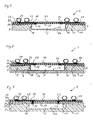
- Figure 5 shows a schematic cross section of an electronic Component 2 of a first embodiment of the invention.
- Components with the same functions as in previous ones Figures are identified by the same reference numerals and will not be discussed separately.
- a rewiring structure is on the second plastic layer 11 19 arranged, the vias 22 to the contact areas 16 of the active top side 15 of the semiconductor chip 5 having.
- the contact areas 16 are as surface contacts educated.
- the rewiring structure 19 that is on the Plastic layer 11 deposited in a chemical process has rewiring lines 23, which from the Through contacts 22 lead to external contact surfaces 29. These external contact areas 29 are outside the area of the semiconductor chip 5 arranged on the plastic plate 3 and carry External contacts 24 in the form of solder balls. Such an arrangement the external contact 24 is also referred to as a "fan-out".
- Figure 6 shows a schematic cross section of an electronic Component 2 of a second embodiment of the invention.
- Components with the same functions as in the previous ones Figures are identified by the same reference numerals and not specifically discussed.
- the second embodiment of the invention differs from the first embodiment of the invention shown in FIG in that the lower region 8 of the first plastic layer 7 is completely networked, so that a Carrier plate made of plastic.
- a metallic one Base plate is used to manufacture such an electronic Component 2 in contrast to the electronic component 2 the first embodiment is not required.
- the completely cross-linked lower area 8 forms a self-supporting Dimensionally stable basis on which the semiconductor chip 5 is aligned and is arranged.
- the upper area 9 of the first Plastic layer 7 is the first before curing Plastic layers 7 and 11 only pre-crosslinked, so that when the semiconductor chip 5 penetrates into the first plastic layer 7 a bead 10 around the edges 18 of the Semiconductor chips 5 are formed.
- the second plastic layer 11 is as a balancing mass on the upper surface 13 of the first plastic layer 7.
- This second Plastic layer 11 forms a flat top surface 25, on which a solder resist layer 30 is arranged is.
- the arrangement and structure of the external contact surfaces and the external contacts correspond to the first shown in FIG. 5 Embodiment.
- Figure 7 shows a schematic cross section of an electronic Component 2 of a third embodiment of the invention.
- Components with the same functions as in the previous ones Figures are identified by the same reference numerals and not specifically discussed.
- the semiconductor chip 5 of the electronic component 2 of the third Embodiment of the invention is also passive with its Back 17 fixed in the first plastic layer 7.
- the third embodiment of the electronic component 2 differs different from the first two embodiments that 5 and 6, characterized in that the contact areas 16 of the semiconductor chip 5 have no surface contacts. Rather, the rewiring structure 19 has contact areas 16 of the semiconductor chip 5 is electrically connected, the inflated flip chip contacts in the form of contact balls, Have contact bumps, contact pillars or contact heads.
- An insulation layer is used to compensate for the height of these flip-chip contacts 31 on the upper side interface 25 of the second plastic layer 11 applied.
- On the insulation layer 31 is a further insulation layer 32 with vias 22 arranged.
- a rewiring structure 19 is arranged is electrically connected to the through contacts 22.
- the order and structure of the external contact surfaces 29 and the external contacts 24 corresponds to that shown in FIGS. 5 and 6 Embodiments.
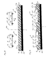
- Figures 8 to 11 show schematic cross sections of Intermediates in the production of a benefit 1 according to a second method example of the invention. components with the same functions as in the previous figures are identified in Figures 8 to 11 with the same reference numerals and not specifically discussed.
- Figure 8 shows a schematic cross section through a first Plastic layer 7 on a base plate 12.
- the first Plastic layer 7 has a lower region 8 which is more networked than an upper area 9.
- the dashed Line 33 marked the transition from the stronger cross-linked lower area 8 to the less cross-linked upper region 9.
- a vertical dash-dotted line in FIG Line 34 marks the boundary between two component positions 4, above each of which a semiconductor chip 5 is aligned in this way is that it is in the direction of arrow A with its active Top 15 and the contact areas 16 in the first plastic layer 7 can be introduced.
- the plastic layer is due to its pre-cross-linked state 7 solid at room temperature and reaches a partially viscous State in the more networked lower area 8 and a lower viscosity state in the upper range 9 when the first plastic layer 7 is heated to temperatures between 90 and 120 ° C. After warming up the first Plastic layer 7 to such a temperature the semiconductor chips 5 with their active tops 15 in Arrow direction A introduced into the first plastic layer 7.
- Figure 9 shows a schematic cross section through the first Plastic layer 7 after embedding the semiconductor chips 5 into the first plastic layer 7 at the component positions 4 of benefit.
- a bead 10 forms in the upper area 9 of the first plastic layer 7 made of each semiconductor chip 5 surrounds in its edge regions 18 and thus the Semiconductor chip 5 fixed in the component positions 4 of the benefit.
- the semiconductor chips 5 are introduced into the first Plastic layer 7 touch the contact areas 16 of the semiconductor chips 5 the base plate 12.
- By further heating the first plastic layer 7 to temperatures between 120 ° C and 350 ° C for 2 minutes to 30 minutes becomes the first Plastic layer 7 completely cross-linked and forms one interface 13 on the upper side.
- FIG. 10 shows a cross section through a panel 1 the application of a second plastic layer 11.
- the second Plastic layer 11 covered the second Plastic layer 11 not the active top 15 of the Semiconductor chips 5, but the passive rear sides 17 of the Semiconductor chips 5.
- the passive rear sides 17 protected from mechanical damage.
- the second plastic layer 11 is under Release of the passive rear sides 17 of the semiconductor chips 5 applied.
- the possibility of heat sinks directly on the passive rear sides 17 of the semiconductor chips 5 apply to after completion of the electronic Dissipate components of heat loss during operation.
- FIG 11 shows a schematic cross section through a Benefits 1 after the application of several rewiring layers 20, 21 and 35 on benefit 1 in the component positions 4.
- the metallic base plate is carried out using etching technology. With appropriate surface preparation of the base plate, this will also benefit from the plastic sheet 3 1 while releasing the contact areas 16 of the semiconductor chips 5 subtracted.
- the surface of FIG shown base plate 12 a few 100 nanometers thin coating for example from polytetrafluoroethylene.
Landscapes
- Encapsulation Of And Coatings For Semiconductor Or Solid State Devices (AREA)
- Structures Or Materials For Encapsulating Or Coating Semiconductor Devices Or Solid State Devices (AREA)
Abstract
Description
- Die aktive Oberseite des Halbleiterchips muss während des Einbettprozesses nicht abgedichtet werden, und die Kontaktbereiche des Halbleiterchips werden zuverlässig offen gehalten.
- Für den Aufbau des expandierten Wafers ist nur ein einziger Bestückungsprozess notwendig. Der Prozessablauf ist daher wesentlich vereinfacht und kostengünstig realisierbar.
- Für dieses Konzept kann auf erhöhte Kontaktbereiche des Halbleiterchip wie Kontaktköpfe, Kontaktsäulen, Kontaktbälle und Kontakthöcker verzichtet werden.
- Es werden keine verlorenen Träger verwendet. Der Träger kann kostengünstig in einem Moldprozess hergestellt werden.
- Die Positionierung und Fixierung der Halbleiterchips ist einfach.
- Für dieses Konzept kann auf erhöhte Kontaktbereiche der Halbleiterchips verzichtet werden.
- Wird eine vollständige Einbettung aller Halbleiterchipseiten in das gleiche Material durchgeführt, so wird eine optimale Zuverlässigkeit des Herstellungsprozesses und der elektronischen Bauteile erreicht.
- Die aktive Seite des Halbleiterchips ist beim Einbetten in die erste Kunststoffschicht nicht aufwendig abzudichten.
- Durch die vollständige Einbettung des Halbleiterchips auch oberhalb der aktiven Oberseite des Halbleiterchips wird die Zuverlässigkeit des Aufbaus weiter erhöht, da die Umverdrahtungslagen auf einer einheitlichen Grundfläche aufgebracht werden können. Die weiteren Umverdrahtungs- und Isolationslagen müssen somit nicht bezüglich der Haftung an das Silicium der Halbleiterchips angepaßt werden.
- Die überhöhten Kontakte müssen keine lötfähigen Verbindungen darstellen, da die Halbleiterchips nicht über die Kontakte fixiert werden, sondern über die Kunststoffeinbettmasse der ersten Kunststoffschicht.
- Wird bei dem Transfermoldprozess die Rückseite der Halbleiterchips freigehalten von Kunststoffgussmasse, so kann dort eine zusätzliche Wärmesenke angebracht werden, um eine höhere Verlustleistung beim Betrieb der elektrischen Bauteile ableiten zu können.
- Figur 1
- zeigt einen schematischen Querschnitt durch einen Nutzen im Bereich einer Bauteilposition,
- Figuren 2 bis 4
- zeigen schematische Querschnitte von Zwischenprodukten bei der Herstellung eines Nutzens gemäß eines ersten Verfahrensbeispiels der Erfindung,
- Figur 2
- zeigt einen schematischen Querschnitt durch eine erste Kunststoffschicht, die auf einer Grundplatte angeordnet ist,
- Figur 3
- einen schematischen Querschnitt einer Bauteilposition nach dem Einbetten eines Halbleiterchips in die erste Kunststoffschicht,
- Figur 4
- zeigt einen schematischen Querschnitt durch einen Nutzen nach Aufbringen einer zweiten Kunststoffschicht auf den Nutzen,
- Figur 5
- zeigt einen schematischen Querschnitt eines elektronischen Bauteils einer ersten Ausführungsform der Erfindung,
- Figur 6
- zeigt einen schematischen Querschnitt eines elektronischen Bauteils einer zweiten Ausführungsform der Erfindung,
- Figur 7
- zeigt einen schematischen Querschnitt eines elektronischen Bauteils einer dritten Ausführungsform der Erfindung,
- Figuren 8 bis 11
- zeigen schematische Querschnitte von Zwischenprodukten bei der Herstellung eines Nutzens gemäß eines zweiten Verfahrensbeispiels der Erfindung,
- Figur 8
- zeigt einen schematischen Querschnitt durch eine erste Kunststoffschicht auf einer Grundplatte,
- Figur 9
- zeigt einen schematischen Querschnitt durch die erste Kunststoffschicht nach einem Einbetten von Halbleiterchips in die erste Kunststoffschicht an Bauteilpositionen des Nutzens,
- Figur 10
- zeigt einen schematischen Querschnitt durch einen Nutzen nach dem Aufbringen einer zweiten Kunststoffschicht
- Figur 11
- zeigt einen schematischen Querschnitt durch einen Nutzen nach einem Aufbringen mehrerer Umverdrahtungslagen auf den Bauteilpositionen des Nutzens.
Claims (29)
- Verfahren zur Herstellung eines Nutzens (1) mit mehreren Bauteilpositionen (4) für elektronische Bauteile (2), wobei der Nutzen (1) eine selbsttragende formstabile Kunststoffplatte (3) aufweist, in der in jeder Bauteilposition (4) ein Halbleiterchip (5) eingebettet ist, und wobei das Verfahren folgende Verfahrensschritte aufweist:a) Herstellen einer Trägerplatte (6) und/oder einer ersten Kunststoffschicht (7) aus einer Kunststoffmasse die in einem unteren Bereich (8) stärker vernetzt ist als in einem oberen Bereich (9),b) Aufbringen jeweils eines Halbleiterchips (5) in den Bauteilpositionen (4) des Nutzens (1) unter Bilden eines die Randseiten (18) des Halbleiterchips (5) umgebenden Wulstes (10) aus Kunststoffmasse der ersten Kunststoffschicht (7),c) Aufbringen einer zweiten Kunststoffschicht (11) undd) Bilden einer selbsttragenden formstabilen Kunststoffplatte (3) mit eingebetteten Halbleiterchips (5) durch Aushärten der Kunststoffschichten (7, 11).
- Verfahren nach Anspruch 1,
dadurch gekennzeichnet, dass
beim Herstellen einer Trägerplatte (6) eine auf 120 bis 350 °C aufgeheizte Grundplatte (12) mit der ersten Kunststoffschicht (7) aus einer Kunststoffmasse beschichtet wird, die beim Abkühlen der Trägerplatte (6) mit erster Kunststoffschicht (7) einen zu einer obenseitigen Grenzfläche (13) der ersten Kunststoffschicht (7) hin abnehmenden Vernetzungsgrad ausbildet. - Verfahren nach Anspruch 1,
dadurch gekennzeichnet, dass
beim Herstellen einer Trägerplatte (6) aus einem Vollkunststoff eine erste Kunststoffschicht (7) einer unvernetzten Kunststoffeinbettmasse einem Temperaturgradienten ausgesetzt wird, wobei innerhalb der ersten Kunststoffschicht (7) ein zu obenseitigen Grenzfläche (13) der ersten Kunststoffschicht (7) hin abnehmender Vernetzungsgrad ausgebildet wird, und wobei zur Unterseite (14) in ersten Kunststoffschicht (7) hin ein erster vollständig vernetzter selbstragender formstabiler unterer Bereich (8) hergestellt wird. - Verfahren nach einem der vorhergehenden Ansprüche,
dadurch gekennzeichnet, dass
eine unvernetzte Kunststoffeinbettmasse für die Herstellung der ersten Kunststoffschicht (7) mit kugelförmigen Partikeln von einheitlichem Kugeldurchmesser insbesondere Glaskugeln gefüllt wird. - Verfahren nach einem der vorhergehenden Ansprüche,
dadurch gekennzeichnet, dass
beim Aufbringen jeweils eines Halbleiterchips (5) in den Bauteilpositionen (4) des Nutzens der Halbleiterchip (5) mit seiner aktiven Oberseite (15) und den darauf angeordneten Kontaktbereichen (16) zunächst in den erste Kunststoffschicht (7) unter Bilden eines die Randseiten (18) des Halbleiterchips (5) umgebenden Wulstes (10) aus Kunststoffmasse der ersten Kunststoffschicht (7) eingedrückt wird, bis seine Kontaktbereiche (16) eine Trägerpatte (6) aus Metall berühren, und anschließend die passive Rückseite (17) des Halbleiterchips (5) von der zweiten Kunststoffschicht (11) bedeckt wird. - Verfahren nach einem der Ansprüche 1 bis 4,
dadurch gekennzeichnet, dass
beim Aufbringen jeweils eines Halbleiterchips (5) in den Bauteilpositionen (4) des Nutzens (1) der Halbleiterchip (5) mit seiner passiven Rückseite (17) zunächst in die erste Kunststoffschicht (7) unter Bilden eines die Randseiten (18) des Halbleiterchips (5) umgebenden Wulstes (10) aus Kunststoffmasse der ersten Kunststoffschicht (7) eingedrückt wird, und wobei anschließend die zweite Kunststoffschicht (11) unter Freilassung mindestens der Kontaktbereiche (16) des Halbleiterchips (5), vorzugsweise unter Freilassung der gesamten aktiven Oberseite (15) des Halbleiterchips (5) den Nutzen (1) einebnet. - Verfahren nach einem der vorhergehenden Ansprüche,
dadurch gekennzeichnet, dass
nach dem Aufbringen der zweiten Kunststoffschicht (11) die Kunststoffmasse beider Kunststoffschichten (7, 11) unter Aufheizen vollständig vernetzt werden. - Verfahren nach einem der Ansprüche 1 bis 6,
dadurch gekennzeichnet, dass
nach dem Aufbringen jeweils eines Halbleiterchips (5) in den Bauteilpositionen (4) des Nutzens (1) in die erste Kunststoffschicht (7), die erste Kunststoffschicht (7) unter Aufheizen vollständig vernetzt wird. - Verfahren nach einem der vorhergehenden Ansprüche,
dadurch gekennzeichnet, dass
die zweite Kunststoffschicht (11) auf eine vollständig vernetzte erste Kunststoffschicht (7) mittels eines Transfermoldverfahrens aufgebracht wird. - Verfahren nach einem der Ansprüche 1 bis 8,
dadurch gekennzeichnet, dass
die zweite Kunststoffschicht (11) auf eine vollständig vernetzte erste Kunststoffschicht (7) mittels eines Schleudergussverfahrens aufgebracht wird. - Verfahren nach einem der vorhergehenden Ansprüche,
dadurch gekennzeichnet, dass
zum Aushärten der zweite Kunststoffschicht (11) der Nutzen (1) auf 120 bis 350 °C für 2 bis 30 Minuten erwärmt wird. - Verfahren nach einem der vorhergehenden Ansprüche,
dadurch gekennzeichnet, dass
zum Aushärten der zweiten Kunststoffschicht (11) der Nutzen (1) für einige Sekunden bis zu einigen Minuten mit UV-Licht bestrahlt wird. - Verfahren nach einem der vorhergehenden Ansprüche,
dadurch gekennzeichnet, dass
auf die selbsttragende formstabile Kunststoffplatte (3) in jeder Bauteilposition (4) eine Umverdrahtungsstruktur (19) aufgebracht wird, die mit Kontaktbereichen (16) in des Halbleiterchips (5) elektrisch verbunden ist. - Verfahren nach einem der vorhergehenden Ansprüche,
dadurch gekennzeichnet, dass
ein Freilegen der Kontaktbereiche (16) der Halbleiterchips (5) eines Nutzens (1) mittels eines photolithographischen Schrittes erfolgt. - Verfahren nach einem der vorhergehenden Ansprüche,
dadurch gekennzeichnet, dass
das Aufbringen der Umverdrahtungsstruktur (19) mittels chemischer oder galvanischer Abscheidung eines Metalls erfolgt. - Verfahren nach Anspruch 15,
dadurch gekennzeichnet, dass
das Aufbringen der Umverdrahtungsstruktur (19) mittels galvanischer Abscheidung in drei Stufen erfolgt, indem zunächst eine geschlossene Metallschicht mittels Sputtern aufgebracht wird, anschließend eine Photolackmaske unter Freilassung der gesputterten Schicht in einem Muster der Umverdrahtungsstruktur (19) aufgebracht wird, und schließlich auf der freigelassenen Struktur galvanisch Metall unter Bildung der Umverdrahtungsstruktur (19) abgeschieden wird, wobei nach der Bildung der Umverdrahtungsstruktur (19) die Photolackschicht und die gesputterte Schicht entfernt werden. - Verfahren nach einem der Ansprüche 1 bis 14,
dadurch gekennzeichnet, dass
das Aufbringen der Umverdrahtungsstruktur (19) mittels Drucktechnik erfolgt. - Verfahren nach einem der vorhergehenden Ansprüche,
dadurch gekennzeichnet, dass
weitere Umverdrahtungslagen (20, 21) auf der Kunststoffplatte (3) angeordnet werden, indem im Wechsel Isolationslagen mit Durchkontakten (22) und Isolationslagen mit Umverdrahtungsleitungen (23) auf der mindestens einen Umverdrahtungsstruktur (19) angeordnet werden. - Verfahren nach einem der vorhergehenden Ansprüche,
dadurch gekennzeichnet, dass
Außenkontakte (24) auf eine äußere Umverdrahtungslage (21) des Nutzens (1) aufgebracht werden. - Verfahren zur Herstellung eines elektronischen Bauteils (2), bei dem mit einem Verfahren gemäß einem der Verfahrensansprüche 1 bis 19 ein Nutzen (1) hergestellt wird, wobei weiterhin der Schritt des Vereinzelns von Bereichen des Nutzens (1) an Bauteilposition (4) vorgesehen ist.
- Elektronisches Bauteil mit einem Halbleiterchip (5), wobei das elektronische Bauteil (2) die folgenden Merkmale aufweist:der Halbleiterchip (5) ist in einer mehrschichtigen Kunststoffeinbettmasse eingebettet,der Halbleiterchip (5) ist auf seinen Randseiten (18) bis zu einem Teil seiner Höhe von einer ersten Kunststoffschicht (7) umgeben,die erste Kunststoffschicht (7) weist eine obenseitige Grenzfläche (13) zu einer darüber liegenden zweiten Kunststoffschicht (11) auf,die zweite Kunststoffschicht (11) liegt an Bereichen der Randseiten (18) des Halbleiterchips (5) an, die nicht von der ersten Kunststoffschicht (7) bedeckt sind,die zweite Kunststoffschicht (11) weist eine ebene Oberseite auf, die eine Grenzfläche (25) zu wenigstens einer weiteren Bauteilebene aufweist,oberhalb der zweiten Kunststoffschicht (11) ist wenigstens eine Umverdrahtungsstruktur (19) mit Durchkontakten (22) zwischen Kontaktbereichen (16) des Halbleiterchips (5) und Außenkontakten (24) des elektronischen Bauteils (2) vorgesehen.
- Nutzen mit mehreren Bauteilpositionen (4) für elektronische Bauteile (2) mit jeweils wenigstens einem Halbleiterchip (5), wobei der Nutzen (1) die folgenden Merkmale aufweist:die Halbleiterchips (5) sind auf ihren Randseiten (18) bis zu jeweils einem Teil ihrer Höhe von einer ersten Kunststoffschicht (7) umgeben,die erste Kunststoffschicht (7) weist eine obenseitige Grenzfläche (13) zu wenigstens einer darüber liegenden zweiten Kunststoffschicht (11) auf,die zweite Kunststoffschicht (11) liegt an Bereichen der Randseiten (18) der Halbleiterchips (5) an, die nicht von der ersten Kunststoffschicht (7) bedeckt sind,die zweite Kunststoffschicht (11) weist eine ebene Oberseite auf, die eine Grenzfläche (25) zu wenigstens einer weiteren Bauteilebene bildet,oberhalb der zweiten Kunststoffschicht (11) und/oder oberhalb der Halbleiterchips (5) sind Umverdrahtungsstrukturen (19) mit Durchkontakten (22) zwischen Kontaktbereichen (16) der Halbleiterchips (5) und Außenkontakten (24) elektronischer Bauteile (2) vorgesehen,die erste Kunststoffschicht (7) und/oder die zweite Kunststoffschicht (11) sind wenigstens teilweise zu einer selbststragenden, im wesentlichen formstabilen, mehrschichtigen Kunststoffplatte (3) ausgehärtet.
- Elektronisches Bauteil oder Nutzen nach Anspruch 21 oder Anspruch 22,
dadurch gekennzeichnet, dass
die erste Kunststoffschicht (7) auf einer Kunststoffeinbettmasse basiert, die höhengestaffelt unterschiedliche Vernetzungsgrade aufweist, wobei der höchste Vernetzungsgrad im Bereich (8) einer Grundfläche (26) der ersten Kunststoffschicht (7) angeordnet ist. - Elektronisches Bauteil oder Nutzen nach einem der Ansprüche 21 bis 23,
dadurch gekennzeichnet, dass
die erste Kunststoffschicht (7) auf einer Kunststoffeinbettmasse basiert, die einen vollständig vernetzten Bereich in dem Bereich (8) einer Grundplatte (12) und darüber einen vorvernetzten Bereich (9) aufweist. - Elektronisches Bauteil oder Nutzen nach einem der Ansprüche 21 bis 24,
dadurch gekennzeichnet, dass
die erste Kunststoffschicht (7) kugelförmige Partikel insbesondere aus Glas aufweist, die als Abstandshalter für die Halbleiterchips (5) in der ersten Kunststoffschicht (7) einen einheitlichen vorgegebenen Durchmesser aufweisen. - Elektronisches Bauteil oder Nutzen nach einem der Ansprüche 21 bis 25,
dadurch gekennzeichnet, dass
die zweite Kunststoffschicht (11) als einebnende Ausgleichsmasse ein Polyimidharz aufweist. - Elektronisches Bauteil oder Nutzen nach einem der Ansprüche 21 bis 26,
dadurch gekennzeichnet, dass
die Umverdrahtungsstruktur (19) eine Haftschicht auf den Grenzflächen zu der Kunststoffplatte (3) aufweist. - Elektronisches Bauteil oder Nutzen nach einem der Ansprüche 21 bis 27,
dadurch gekennzeichnet, dass
die Halbleiterchips (5) mit ihren aktiven Oberseiten (15) in der ersten Kunststoffschicht (7) eingebettet sind und ihre passiven Rückseiten (17) von der zweiten Kunststoffschicht (11) bedeckt sind. - Elektronisches Bauteil oder Nutzen nach einem der Ansprüche 21 bis 27 ,
dadurch gekennzeichnet, dass
die Halbleiterchips (5) mit ihren aktiven Oberseiten (15) aus der ersten Kunststoffschicht (7) herausragenden, und wobei ihre passiven Rückseiten (17) in der ersten Kunststoffschicht (7) eingebettet sind.
Applications Claiming Priority (2)
| Application Number | Priority Date | Filing Date | Title |
|---|---|---|---|
| DE10240460A DE10240460A1 (de) | 2002-08-29 | 2002-08-29 | Universelles Halbleitergehäuse mit vorvernetzten Kunststoffeinbettmassen und Verfahren zur Herstellung desselben |
| DE10240460 | 2002-08-29 |
Publications (2)
| Publication Number | Publication Date |
|---|---|
| EP1398828A2 true EP1398828A2 (de) | 2004-03-17 |
| EP1398828A3 EP1398828A3 (de) | 2010-03-03 |
Family
ID=31502267
Family Applications (1)
| Application Number | Title | Priority Date | Filing Date |
|---|---|---|---|
| EP03017505A Withdrawn EP1398828A3 (de) | 2002-08-29 | 2003-08-04 | Halbleitergehäuse mit vorvernetzten Kunststoffeinbettmassen und Verfahren zur Herstellung desselben |
Country Status (3)
| Country | Link |
|---|---|
| US (2) | US20040043515A1 (de) |
| EP (1) | EP1398828A3 (de) |
| DE (1) | DE10240460A1 (de) |
Cited By (1)
| Publication number | Priority date | Publication date | Assignee | Title |
|---|---|---|---|---|
| US8431063B2 (en) | 2005-10-17 | 2013-04-30 | Intel Mobile Communications GmbH | Heat treatment for a panel and apparatus for carrying out the heat treatment method |
Families Citing this family (15)
| Publication number | Priority date | Publication date | Assignee | Title |
|---|---|---|---|---|
| US7210635B2 (en) * | 2004-07-02 | 2007-05-01 | Caterpillar Inc | System and method for encapsulation and protection of components |
| US7390551B2 (en) * | 2004-07-02 | 2008-06-24 | Caterpillar Inc. | System and method for encapsulation and protection of components |
| US7829998B2 (en) | 2007-05-04 | 2010-11-09 | Stats Chippac, Ltd. | Semiconductor wafer having through-hole vias on saw streets with backside redistribution layer |
| US8445325B2 (en) | 2007-05-04 | 2013-05-21 | Stats Chippac, Ltd. | Package-in-package using through-hole via die on saw streets |
| US7723159B2 (en) * | 2007-05-04 | 2010-05-25 | Stats Chippac, Ltd. | Package-on-package using through-hole via die on saw streets |
| US20090160053A1 (en) * | 2007-12-19 | 2009-06-25 | Infineon Technologies Ag | Method of manufacturing a semiconducotor device |
| US8264085B2 (en) | 2008-05-05 | 2012-09-11 | Infineon Technologies Ag | Semiconductor device package interconnections |
| US8421226B2 (en) * | 2010-02-25 | 2013-04-16 | Infineon Technologies Ag | Device including an encapsulated semiconductor chip and manufacturing method thereof |
| US8241964B2 (en) | 2010-05-13 | 2012-08-14 | Stats Chippac, Ltd. | Semiconductor device and method of embedding bumps formed on semiconductor die into penetrable adhesive layer to reduce die shifting during encapsulation |
| US9013017B2 (en) | 2012-10-15 | 2015-04-21 | Stmicroelectronics Pte Ltd | Method for making image sensors using wafer-level processing and associated devices |
| US9059058B2 (en) | 2012-10-22 | 2015-06-16 | Stmicroelectronics Pte Ltd | Image sensor device with IR filter and related methods |
| US20150342069A1 (en) * | 2014-05-20 | 2015-11-26 | Freescale Semiconductor, Inc. | Housing for electronic devices |
| US10580710B2 (en) | 2017-08-31 | 2020-03-03 | Micron Technology, Inc. | Semiconductor device with a protection mechanism and associated systems, devices, and methods |
| US10475771B2 (en) | 2018-01-24 | 2019-11-12 | Micron Technology, Inc. | Semiconductor device with an electrically-coupled protection mechanism and associated systems, devices, and methods |
| US10381329B1 (en) * | 2018-01-24 | 2019-08-13 | Micron Technology, Inc. | Semiconductor device with a layered protection mechanism and associated systems, devices, and methods |
Citations (8)
| Publication number | Priority date | Publication date | Assignee | Title |
|---|---|---|---|---|
| EP0915505A1 (de) | 1997-11-06 | 1999-05-12 | Sharp Kabushiki Kaisha | Packung für eine Halbleiteranordnung, Verfahren zu ihrer Herstellung und Leiterplatte dafür |
| US5930599A (en) | 1996-02-19 | 1999-07-27 | Matsushita Electric Industrial Co., Ltd. | Semiconductor device and method of manufacturing the same |
| US5990546A (en) | 1994-12-29 | 1999-11-23 | Nitto Denko Corporation | Chip scale package type of semiconductor device |
| JP2000277568A (ja) | 1999-01-19 | 2000-10-06 | Murata Mfg Co Ltd | 電子部品の実装方法及び実装構造 |
| JP2001196522A (ja) * | 2000-01-12 | 2001-07-19 | Nec Corp | プリント配線板およびマルチチップ・モジュール |
| US20020004258A1 (en) | 1999-09-03 | 2002-01-10 | Seiko Epson Corporation | Semiconductor device and method of fabricating the same, circuit board, and electronic equipment |
| JP2002110714A (ja) * | 2000-10-02 | 2002-04-12 | Sony Corp | チップ集積ボード及びその製造方法、チップ状電子部品及びその製造方法、電子機器及びその製造方法 |
| US20020105073A1 (en) | 2000-09-29 | 2002-08-08 | Smith John W. | Low cost and compliant microelectronic packages for high i/o and fine pitch |
Family Cites Families (18)
| Publication number | Priority date | Publication date | Assignee | Title |
|---|---|---|---|---|
| CN87107692A (zh) | 1986-11-13 | 1988-05-25 | Mt化学公司 | 半导体器件的制造方法 |
| JP2579937B2 (ja) * | 1987-04-15 | 1997-02-12 | 株式会社東芝 | 電子回路装置およびその製造方法 |
| US5032543A (en) * | 1988-06-17 | 1991-07-16 | Massachusetts Institute Of Technology | Coplanar packaging techniques for multichip circuits |
| JPH06502744A (ja) | 1991-03-27 | 1994-03-24 | インテグレイテッド システム アセンブリース コーポレーション | マルチチップ集積回路パッケージ及びモジュール |
| US5144747A (en) * | 1991-03-27 | 1992-09-08 | Integrated System Assemblies Corporation | Apparatus and method for positioning an integrated circuit chip within a multichip module |
| US5353498A (en) * | 1993-02-08 | 1994-10-11 | General Electric Company | Method for fabricating an integrated circuit module |
| US5306670A (en) * | 1993-02-09 | 1994-04-26 | Texas Instruments Incorporated | Multi-chip integrated circuit module and method for fabrication thereof |
| DE4427309C2 (de) | 1994-08-02 | 1999-12-02 | Ibm | Herstellung eines Trägerelementmoduls zum Einbau in Chipkarten oder andere Datenträgerkarten |
| WO1997022993A1 (en) * | 1995-12-15 | 1997-06-26 | International Business Machines Corporation | Electronic package with spacer means |
| KR100253116B1 (ko) * | 1997-07-07 | 2000-04-15 | 윤덕용 | Le방법을 이용한 칩사이즈 패키지의 제조방법 |
| US5923958A (en) * | 1998-05-28 | 1999-07-13 | Pan Pacific Semiconductor Co., Ltd. | Method for semiconductor chip packaging |
| US5972735A (en) * | 1998-07-14 | 1999-10-26 | National Starch And Chemical Investment Holding Corporation | Method of preparing an electronic package by co-curing adhesive and encapsulant |
| US6515355B1 (en) * | 1998-09-02 | 2003-02-04 | Micron Technology, Inc. | Passivation layer for packaged integrated circuits |
| US6239482B1 (en) * | 1999-06-21 | 2001-05-29 | General Electric Company | Integrated circuit package including window frame |
| JP3818623B2 (ja) | 1999-09-21 | 2006-09-06 | 住友ベークライト株式会社 | 半導体装置の組立方法 |
| ES2257353T3 (es) * | 2000-04-21 | 2006-08-01 | Jsr Corporation | Composicion de resina termoplastica. |
| TW497236B (en) * | 2001-08-27 | 2002-08-01 | Chipmos Technologies Inc | A soc packaging process |
| DE10213296B9 (de) * | 2002-03-25 | 2007-04-19 | Infineon Technologies Ag | Elektronisches Bauteil mit einem Halbleiterchip, Verfahren zu seiner Herstellung und Verfahren zur Herstellung eines Nutzens |
-
2002
- 2002-08-29 DE DE10240460A patent/DE10240460A1/de not_active Withdrawn
-
2003
- 2003-08-04 EP EP03017505A patent/EP1398828A3/de not_active Withdrawn
- 2003-08-29 US US10/651,856 patent/US20040043515A1/en not_active Abandoned
-
2006
- 2006-07-24 US US11/491,746 patent/US7517722B2/en not_active Expired - Fee Related
Patent Citations (8)
| Publication number | Priority date | Publication date | Assignee | Title |
|---|---|---|---|---|
| US5990546A (en) | 1994-12-29 | 1999-11-23 | Nitto Denko Corporation | Chip scale package type of semiconductor device |
| US5930599A (en) | 1996-02-19 | 1999-07-27 | Matsushita Electric Industrial Co., Ltd. | Semiconductor device and method of manufacturing the same |
| EP0915505A1 (de) | 1997-11-06 | 1999-05-12 | Sharp Kabushiki Kaisha | Packung für eine Halbleiteranordnung, Verfahren zu ihrer Herstellung und Leiterplatte dafür |
| JP2000277568A (ja) | 1999-01-19 | 2000-10-06 | Murata Mfg Co Ltd | 電子部品の実装方法及び実装構造 |
| US20020004258A1 (en) | 1999-09-03 | 2002-01-10 | Seiko Epson Corporation | Semiconductor device and method of fabricating the same, circuit board, and electronic equipment |
| JP2001196522A (ja) * | 2000-01-12 | 2001-07-19 | Nec Corp | プリント配線板およびマルチチップ・モジュール |
| US20020105073A1 (en) | 2000-09-29 | 2002-08-08 | Smith John W. | Low cost and compliant microelectronic packages for high i/o and fine pitch |
| JP2002110714A (ja) * | 2000-10-02 | 2002-04-12 | Sony Corp | チップ集積ボード及びその製造方法、チップ状電子部品及びその製造方法、電子機器及びその製造方法 |
Cited By (1)
| Publication number | Priority date | Publication date | Assignee | Title |
|---|---|---|---|---|
| US8431063B2 (en) | 2005-10-17 | 2013-04-30 | Intel Mobile Communications GmbH | Heat treatment for a panel and apparatus for carrying out the heat treatment method |
Also Published As
| Publication number | Publication date |
|---|---|
| EP1398828A3 (de) | 2010-03-03 |
| US7517722B2 (en) | 2009-04-14 |
| US20060258046A1 (en) | 2006-11-16 |
| DE10240460A1 (de) | 2004-03-11 |
| US20040043515A1 (en) | 2004-03-04 |
Similar Documents
| Publication | Publication Date | Title |
|---|---|---|
| EP2259311B1 (de) | Verfahren zum Einbetten zumindest eines Bauelements in einem Leiterplattenelement | |
| DE102011001402B4 (de) | Verfahren zum Herstellen eines Halbleiter-Bauelements | |
| DE10213296B4 (de) | Elektronisches Bauteil mit einem Halbleiterchip, Verfahren zu seiner Herstellung und Verfahren zur Herstellung eines Nutzens | |
| DE102010042567B3 (de) | Verfahren zum Herstellen eines Chip-Package und Chip-Package | |
| DE102011001405B4 (de) | Halbleiter-Kapselung und Stapel von Halbleiterkapselungen sowie Verfahren zur Herstellung einer Halbleiter-Kapselung | |
| DE69525280T2 (de) | Herstellungsverfahren einer mit Anschlusshöckern versehenen Halbleiteranordnung vom Filmträgertyp | |
| DE4008624C2 (de) | ||
| DE102011000836B4 (de) | Bauelement mit einem eingekapselten Halbleiterchip und Herstellungsverfahren | |
| DE102008038175B4 (de) | Halbleiteranordnung und Verfahren zur Herstellung von Halbleiteranordnungen | |
| DE102011001556B4 (de) | Herstellungsverfahren für einen gekapselten Halbleiterchip mit externen Kontaktpads | |
| DE10240460A1 (de) | Universelles Halbleitergehäuse mit vorvernetzten Kunststoffeinbettmassen und Verfahren zur Herstellung desselben | |
| DE102009042920B4 (de) | Verfahren zur Herstellung eines Halbleiter-Bauelements und Verfahren zur Herstellung mehrerer Halbleiter-Bauelemente | |
| DE102010036678A1 (de) | Multichip-Modul und Verfahren zu seiner Herstellung | |
| DE102014117594A1 (de) | Halbleiter-Package und Verfahren zu seiner Herstellung | |
| DE102010041129A1 (de) | Multifunktionssensor als PoP-mWLP | |
| DE102013102230A1 (de) | Halbleiterpackages und Verfahren zu deren Ausbildung | |
| DE102016124270A1 (de) | Halbleiter-package und verfahren zum fertigen eines halbleiter-package | |
| DE102017215797B4 (de) | Verfahren zur Herstellung von gehäusten Halbleitervorrichtungen | |
| DE102016123129B4 (de) | Elektronische Komponente und Verfahren | |
| DE102013111772B4 (de) | Halbleiterbauelemente und Verfahren zur Herstellung von Halbleiterbauelementen | |
| DE10221646A1 (de) | Verfahren zur Verbindung von Schaltungseinrichtungen und entsprechender Verbund von Schaltungseinrichtungen | |
| WO2024061689A1 (de) | Verfahren zum herstellen eines elektronischen bauelements und elektronisches bauelement | |
| DE102019118480A1 (de) | Integriertes schaltungs-package und verfahren | |
| DE102005015036B4 (de) | Verfahren zur Montage eines Chips auf einer Unterlage | |
| DE102016202548B3 (de) | Verfahren zur Herstellung eines elektronischen Bauelements und elektronisches Bauelement |
Legal Events
| Date | Code | Title | Description |
|---|---|---|---|
| PUAI | Public reference made under article 153(3) epc to a published international application that has entered the european phase |
Free format text: ORIGINAL CODE: 0009012 |
|
| AK | Designated contracting states |
Kind code of ref document: A2 Designated state(s): AT BE BG CH CY CZ DE DK EE ES FI FR GB GR HU IE IT LI LU MC NL PT RO SE SI SK TR |
|
| AX | Request for extension of the european patent |
Extension state: AL LT LV MK |
|
| PUAL | Search report despatched |
Free format text: ORIGINAL CODE: 0009013 |
|
| AK | Designated contracting states |
Kind code of ref document: A3 Designated state(s): AT BE BG CH CY CZ DE DK EE ES FI FR GB GR HU IE IT LI LU MC NL PT RO SE SI SK TR |
|
| AX | Request for extension of the european patent |
Extension state: AL LT LV MK |
|
| RIC1 | Information provided on ipc code assigned before grant |
Ipc: H01L 23/31 20060101ALN20100126BHEP Ipc: H01L 21/56 20060101ALI20100126BHEP Ipc: H01L 23/538 20060101AFI20100126BHEP |
|
| RAP1 | Party data changed (applicant data changed or rights of an application transferred) |
Owner name: INFINEON TECHNOLOGIES AG |
|
| 17P | Request for examination filed |
Effective date: 20100506 |
|
| 17Q | First examination report despatched |
Effective date: 20100623 |
|
| AKX | Designation fees paid |
Designated state(s): DE FR IT |
|
| RIC1 | Information provided on ipc code assigned before grant |
Ipc: H01L 23/538 20060101AFI20130709BHEP Ipc: H01L 23/31 20060101ALN20130709BHEP Ipc: H01L 21/56 20060101ALI20130709BHEP |
|
| RIC1 | Information provided on ipc code assigned before grant |
Ipc: H01L 23/31 20060101ALN20130918BHEP Ipc: H01L 23/538 20060101AFI20130918BHEP Ipc: H01L 21/56 20060101ALI20130918BHEP Ipc: H01L 21/60 20060101ALI20130918BHEP |
|
| GRAP | Despatch of communication of intention to grant a patent |
Free format text: ORIGINAL CODE: EPIDOSNIGR1 |
|
| INTG | Intention to grant announced |
Effective date: 20131025 |
|
| STAA | Information on the status of an ep patent application or granted ep patent |
Free format text: STATUS: THE APPLICATION IS DEEMED TO BE WITHDRAWN |
|
| 18D | Application deemed to be withdrawn |
Effective date: 20140305 |