EP1374397B1 - Circuit de reception pour recepteur radio mobile a reglage automatique de gain - Google Patents
Circuit de reception pour recepteur radio mobile a reglage automatique de gain Download PDFInfo
- Publication number
- EP1374397B1 EP1374397B1 EP01962670A EP01962670A EP1374397B1 EP 1374397 B1 EP1374397 B1 EP 1374397B1 EP 01962670 A EP01962670 A EP 01962670A EP 01962670 A EP01962670 A EP 01962670A EP 1374397 B1 EP1374397 B1 EP 1374397B1
- Authority
- EP
- European Patent Office
- Prior art keywords
- signal
- signal strength
- pgc
- amplifier
- stage
- Prior art date
- Legal status (The legal status is an assumption and is not a legal conclusion. Google has not performed a legal analysis and makes no representation as to the accuracy of the status listed.)
- Expired - Lifetime
Links
Images

Classifications
-
- H—ELECTRICITY
- H03—ELECTRONIC CIRCUITRY
- H03G—CONTROL OF AMPLIFICATION
- H03G3/00—Gain control in amplifiers or frequency changers
- H03G3/20—Automatic control
- H03G3/30—Automatic control in amplifiers having semiconductor devices
- H03G3/3089—Control of digital or coded signals
-
- H—ELECTRICITY
- H03—ELECTRONIC CIRCUITRY
- H03G—CONTROL OF AMPLIFICATION
- H03G3/00—Gain control in amplifiers or frequency changers
- H03G3/001—Digital control of analog signals
-
- H—ELECTRICITY
- H03—ELECTRONIC CIRCUITRY
- H03G—CONTROL OF AMPLIFICATION
- H03G3/00—Gain control in amplifiers or frequency changers
- H03G3/20—Automatic control
- H03G3/30—Automatic control in amplifiers having semiconductor devices
- H03G3/3052—Automatic control in amplifiers having semiconductor devices in bandpass amplifiers (H.F. or I.F.) or in frequency-changers used in a (super)heterodyne receiver
Definitions
- the invention relates to a receiving circuit for a mobile radio receiver, in particular a cordless telephone, which is equipped with a controllable amplifier variable gain. Furthermore, the invention relates to a method for processing a received signal in a mobile radio receiver.
- AGC Automatic Gain Control
- signal strength estimation is in the analog signal processing, i. in the signal path before the analog-to-digital converter stage.
- PGC programmable gain control
- the gain setting is derived from a digital control word output from a signal strength estimator located in the digital signal processing area.
- HSP50214B the company HARRIS Semiconductor (Intersil) is known, which has a PGC and the channel selection in the digital signal processing area (using digital filters).
- the PGC consists of a cascade consisting of 36 individual amplifier stages, each with a gain of 2 dB, which can be individually switched on or off.
- the signal strength estimation takes place in the digital domain on the total signal, ie before the channel selection.
- the disadvantage of this module is mainly the high implementation cost of PGC. Further disadvantages can be seen in the likewise complex realization of the external analog-to-digital converter stage and the digital filter arrangement.
- US Pat. No. 6,005,506 A discloses a receiving circuit for a mobile radio receiver in which a variable gain controllable amplifier, an analogue-to-digital converter stage, a digital filter arrangement for channel selection and a signal strength estimator for determining the signal strength in the selected useful channel are arranged in the signal path ,
- the amplifier is controllable in response to the useful channel signal strength determined by the signal strength estimator.
- the receiving circuit comprises a controllable amplifier 32, an analog-to-digital converter stage 11-1 and 11-2, a digital filter arrangement 12-1 to 12-3 and a signal strength estimator 104.
- An evaluation unit 105 sets the gain of the amplifier 32 on the basis of the estimated value of Signal strength in the selected traffic channel.
- the signal filter arrangement 12-1 to 12-3 consists of band-pass filters for channel selection.
- the invention has for its object to provide a receiving circuit for a mobile radio receiver with a channel selection in the digital signal processing area, which should be ensured that at the input of the analog-to-digital converter stage applied signal does not overdrive the analog-to-digital converter stage. Furthermore, a corresponding method for processing a received signal in a mobile radio receiver is to be specified.
- the signal strength of the broadband input signal drops, while the signal strength of the useful channel signal remains constant, only slightly decreases or even increases. In these cases, an adjustment of the amplifier for the purpose of a level adjustment can be omitted.
- the gain must be readjusted immediately at each drop in the total signal strength, because it must be assumed that the channel-selected useful signal is affected by the loss of energy.
- the circuit has a very good control behavior.
- An advantageous embodiment of the receiving circuit according to the invention is characterized in that the controllable amplifier, in particular PGC, is composed of several amplifier stages, that the receiving circuit comprises an evaluation device which is informed of the signal strength estimator determined useful channel signal strength, and that a Connection of an amplifier stage is always made when the evaluation determines that a predetermined signal-to-noise ratio is exceeded in the received signal.
- This form of level adjustment ensures that the connection of a further amplifier stage of the amplifier is only requested if it is actually required for reasons of too low a signal quality (expressed by the signal-to-noise ratio). This ensures that a minimum number of gain switching points occur over the entire dynamic range. This in turn makes it possible to minimize the number of gain stages of the amplifier. Since the implementation complexity and the cost of the amplifier (eg PGC) is determined by the number of stages, this allows the implementation of a very low-cost hardware for level matching before analog-to-digital conversion.
- this protection against overdriving of the analog-to-digital converter stage is achieved in that the receiving circuit further comprises a memory means in which signal strength values for the useful channel and adjacent channels can be stored, and in that the evaluation device can read out the signal strength values stored in the memory means .
- the receiving circuit further comprises a memory means in which signal strength values for the useful channel and adjacent channels can be stored, and in that the evaluation device can read out the signal strength values stored in the memory means .
- An additional signal strength estimator may be omitted before (in the case of an AGC) or behind (in the case of a PGC) the analog-to-digital converter stage.
- controllable amplifier comprises between three and six, in particular four, amplifier stages.
- a further advantageous embodiment of the invention is characterized in that the analog-to-digital converter stage is implemented by a delta-sigma converter.
- This type of converter is characterized by a reduced implementation cost compared to the commonly used flash digital-to-analog converter.
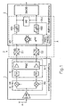
- Fig. 1 shows in the form of a block diagram in an exemplary manner the structure of a receiving circuit according to the invention.
- the receiving circuit can be used in cordless digital communication systems (e.g., DECT, WDCT, Bluetooth, SWAP, WLAN, etc.).
- the receiving circuit has a receiving side arranged circuit part 1, in which an analog signal processing is performed, an output side arranged circuit part 2, in which the signal processing is digital, and an analog-to-digital converter stage 3, which in the signal path between the analog circuit part 1 and the digital circuit part 2 is provided.
- a radio signal is picked up by an antenna A and fed to a low-noise input amplifier LNA.
- the gain of the LNA can be made adjustable so that the LNA simultaneously represents the foremost stage of the PGC as shown in FIG.
- the input amplifier LNA amplifies the high-frequency antenna signal.
- An output of the amplifier LNA is supplied to a high-frequency mixer M.
- the RF mixer M comprises two mixers M1, M2 which downconvert the amplified high frequency signal to an intermediate frequency range.
- the mixers M1 and M2 are operated in a known manner with a phase offset of 90 ° with an adjustable mixing frequency. At their outputs is in each case an analog intermediate frequency signal (in-phase branch or quadrature branch) ready.
- the RF mixer M is followed by a unit E for prefiltering and amplification of the received from the RF mixer M intermediate frequency signals.
- the unit E has on the input side for each signal branch on an analog low-pass filter TP, which is also referred to in the art as an anti-aliasing filter.
- the outputs of the two low-pass filters TP are each supplied to a PGC.
- the gain of both PGCs is variable and can be adjusted via a common control signal input to which a common control signal S is applied. Since the control signal S is a digital control word, the setting of the gain of the PGC is also referred to as programming.
- Each PGC is constructed in a manner not shown from a plurality of series-connected amplifier stages of a constant but not necessarily identical gain. The gain adjustment then takes place by simply switching an amplifier stage on or off in response to an instruction by the control signal word S.
- the outputs of the two PGC simultaneously represent the outputs of the analog circuit part 1.
- the said outputs are each supplied to an analog-to-digital converter 3.1 or 3.2.
- the two analog-to-digital converters 3.1 and 3.2 realize the analog-to-digital converter stage 3.
- a digital intermediate frequency signal is output whose bandwidth is limited only by the low-pass filter TP. This means that the digital intermediate-frequency signals output by the analog-to-digital converter stage 3 can cover several, in particular also all available user channels.
- the outputs of the analog-to-digital converters 3.1 and 3.2 are fed to a complex digital intermediate frequency (IF) mixer dM.
- the digital IF mixer dM multiplies the digital signal values by a phase signal exp (jw 0 t) of the angular frequency w 0 .
- t denotes the time and j the imaginary unit.
- the digital IF mixer dM shifts the frequency position of the received digital signal by the ia fixed frequency w 0 / 2 ⁇ .
- the digital mixer dM has two outputs at which wideband digital receive signals of the I-branch and the Q-branch are output.
- a channel selection and decimation stage KS1 or KS2 is provided in each signal branch.
- the two channel selection and decimation KS1, KS2 are identical and will be described in more detail in connection with FIG.
- a digital signal is output, whose bandwidth is limited to the channel bandwidth and compared to the sampling rate of the analog-to-digital converters 3.1 and 3.2 has lowered signal rate (data symbol rate).
- the tuning of this signal to a desired Traffic channel is carried out by means of the analog, adjustable mixers M1, M2.
- the two outputs of the channel selection and decimation KS1, KS2 are fed into a digital demodulator DMOD, which demodulates the signals according to the standard underlying the signal transmission in a known manner.
- the demodulation may include, for example, adaptive channel estimation, equalization, channel decoding, etc.
- the demodulated signal is subsequently suitably further processed, i. e.g. deinterleaved, source decoded, converted into an analog signal, amplified and fed to a suitable output unit (e.g., speaker, monitor).
- the outputs of the two channel selection and decimation stages KS1, KS2 are also connected to a power estimator PE.
- the power estimator PE makes a power estimation in the traffic channel based on the obtained digital signals of the I and Q branches.
- the result of this power estimation i.e., a digitally coded value indicating the power measured in the payload channel
- PGC programmer PGC-PROG via a data line DL1.
- the PGC programming unit PGC-PROG controls the PGC. In the event that the PGC is made up of several amplifier stages that can be switched on and off, the PGC programming unit PGC-PROG tells the PGC how many amplifier stages are to be activated. If the amplifier stages have different gains, the control signal issued by the PGC programmer PGC-PROG also notifies the PGC, which of the amplifier stages are to be activated or deactivated.
- the switching of the PGC to a greater gain always takes place when a predetermined minimum signal-to-noise ratio in the bandwidth-limited useful channel signal is exceeded.
- a threshold can be defined which ensures that a maximum bit error rate, e.g. at the output of the digital demodulator DMOD is not exceeded.
- the signal-to-noise ratio is calculated in the PGC programming unit PGC-PROG from the power value communicated via the data line DL1 and a noise power.
- the noise power (or noise level) is determined by the input noise of the receiver and the inherent noise of the analog circuit part 1 of the receiver, ie the dimensioning of the analog signal path.
- the noise power depends on the selected gain of the PGC.
- a value for the corresponding noise power is stored in the PGC programming unit PGC-PROG.
- the signal-to-noise ratio occurring in the useful channel is then determined by quotienting the power value output by the power estimator PE with the noise power value stored in the PGC programming unit PGC-PROG with respect to the selected programming calculated. Another possibility is to determine the noise power in the user channel by direct measurement.
- FIGS. 3a and 3b the logarithmic signal-to-noise ratio SNR (in dB) is plotted against the logarithmic ratio of the level of the input signal before the PGC to the maximum allowable signal level of that input signal (in dBm).
- the minimum permissible signal-to-noise ratio is 20 dB in this example.
- the connection of an amplifier stage takes place whenever the signal-to-noise ratio becomes less than 20 dB, i. at the switching points P1, P2, P3.
- a PGC comprising four amplifier stages is sufficient.
- Fig. 3b the level of the signal in the useful channel behind the channel selection and decimation KS1 or KS2 (curve K1), the level of the (broadband) total signal behind the PGC (curve K2) and the (gain-dependent) noise level (curve K3) in the useful channel compared to the level of the input signal before the PGC (in dBm in each case) (the two diagrams of FIGS. 3a and 3b have a common x-axis). It becomes clear that with each connection of an amplifier stage, a sudden increase in the useful signal level (curve K1) occurs. The opposite applies to the deactivation of an amplifier stage with increasing level of the input signal.
- the curve K3 makes it clear that the noise level in the useful channel does not necessarily have to reduce when an amplifier stage is switched off. Since an amplifier stage also amplifies the noise of the signal paths in front of it lying function blocks, is indeed when switching off an amplifier stage basically to expect a reduction of the total noise. At point P3, however, this effect is not significant since there (in the particular example illustrated) the gain in the foremost amplifier stage is changed. At point P2, a noise reduction is detected as a middle amplifier stage is taken out. The gain adjustment at point P1 is done (in the concrete example) by a change in the gain of a switch capacitor realization that forms the rearmost amplifier stage. This amplifier stage has a much larger inherent noise with a small amplifier setting, so that the resulting total noise in the reception path increases (even).
- the magnitude of the switched gain (when the input signal level drops) must be selected so that the overall broadband signal behind the PGC does not lead to overmodulation of the analog-to-digital converters 3.1 or 3.2. Since the overall signal behind the PGC is composed of the useful signal and possible (possibly larger) signals in adjacent channels, it is for a reliable prevention of overdriving at the input of the analog-to-digital converter 3.1. or 3.2 is not sufficient to evaluate only the power in the payload signal (according to the information output by the power estimator PE).
- One way to prevent overdriving the analog-to-digital converter 3.1, 3.2 is to remove the signal power of adjacent channels of a channel list. To explain this possibility, reference is made to FIGS. 2 and 4.
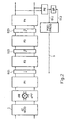
- FIG. 2 shows the detail A of the receiving circuit shown in FIG. 1, which is bordered by a dashed line.
- the digital circuit part 2 has a memory SP whose input is connected to the output of the power estimator PE. An exit of the memory SP is connected to the PGC programming unit PGC-PROG via a data line DL2.
- a so-called RSSI scan is performed at regular intervals, in which the signal strength (or power) is determined in all available channels and registered in a list, which is managed by the memory SP.
- An example of such a channel list is shown in FIG. The example is based on an FDMA / TDMA multiple access system with ten available frequency bands (channels) and twelve time slots. In the example shown, a useful signal in the frequency band 5 is now to be received within the time slot 5.
- the signal strength values of all available channels which were determined by the power estimator PE in the RSSI scan, are entered in the unit dBm. Channels with signal strengths less than e.g. -96 dBm are marked as free channels in the list. Channels 1 to 4, 6, 9 and 10 are therefore free. Channels in which larger signals are measured (channels 5, 7, 8) are marked as occupied.
- the channel list is only used to find out which channels are free and thus available for a possible handover.
- the information contained in the channel list is also used to exclude an override of the input of the analog-to-digital converter stage 3.
- the PGC programming unit PGC-PROG reads out the signal strength values entered in the channel list for the time slot 5 and determines the largest signal value. in the present case -30 dBm in the channel 8.
- the gain of the PGC is then set via the control signal S so that even taking into account the largest interference signal (channel 8) no Override at the input of the analog-to-digital converter stage 3 occurs.
- that amplifier stage can be selected and switched on, which has the maximum gain among those amplifier stages that would cause a clipping no overdriving of the analog-to-digital converter 3.1 and 3.2, respectively.
- Shutdown of a transmitter stage may also be performed based on the signal strength values stored in the channel list whenever a signal level value appears in the list indicating that the analog to digital converter stage is overdriven, i. which takes a maximum value. If an additional signal level estimator is provided at the input (for an AGC) or at the output (for a PGC) of the analog-to-digital converter stage 3, of course, this can also be used to initiate a shutdown of an amplifier stage.
- the analog-to-digital converter stage 3 is shown in more detail in connection with the low-pass filters TP of FIG.
- the analog-to-digital conversion is performed by a delta-sigma modulator MOD of order L and the channel filtering by a cascade consisting of three decimation stages DZ1, DZ2, DZ3 and four filter stages F1, F2, F3, F4.
- the filter stages F1, F2, F3, F4 and the decimation stages DZ1, DZ2, DZ3 are arranged alternately, so that from filter stage to filter stage in each case a sampling rate reduction takes place for example by a factor of 2.
- the filter stage F1 arranged on the input side in the signal path can be realized by a so-called sinc k filter of the L + 1th order.
- the two subsequent filter stages F2 and F3 are realized by minimal-phase bridge wave or wave digital filters.
- the second filter stage F2 may be a bifilar wave digital filter and the third filter stage F3 may be a bridge wave digital filter.
- the output-side filter stage F4 can be realized in the form of a simple attenuation filter (equalizer filter). This filter F4 serves to compensate for group delay distortions caused by the upstream recursive filters.
- the minimum-phase bridge wave or wave digital filters F2 and F3 are characterized in that they have a minimum group delay.
- the implementation cost of these filters F2 and F3 is significantly lower than that of FIR filter.
- the illustrated filter concept thus has clear advantages over a filter cascade using FIR filters.
- Fig. 2 delta-sigma modulator MOD, F1, DZ1, F2, DZ2, F3, DZ3, F4 beyond a reduced implementation effort in the field of analog signal processing (ie in the delta-sigma modulator MOD).
- a data control line running from the PGC programmer PGC-PROG to the low-noise input amplifier is designated DL3 in FIG.
Landscapes
- Circuits Of Receivers In General (AREA)
- Amplifiers (AREA)
- Control Of Amplification And Gain Control (AREA)
Claims (10)
- Circuit de réception pour un récepteur de téléphonie mobile, dans lequel il est monté dans le trajet du signal dans l'ordre mentionné dans ce qui suit:- un amplificateur (PGC) pouvant être régulé de gain variable,- un étage (3) de convertisseur analogique-numérique,- un montage (KS1, KS2) de filtre numérique pour la sélection de canal, et- un évaluateur (PE) de l'intensité du signal pour déterminer l'intensité du signal dans le canal utile sélectionné, et dans lequel- l'amplificateur (PGC) peut être régulé en fonction de l'intensité du signal du canal utile déterminé par l'évaluateur de l'intensité du signal,caractérisé- en ce que le circuit de réception comporte un moyen (SP) de mémoire, dans lequel des valeurs d'intensité du signal pour le canal utile déterminées par l'évaluateur (PE) d'intensité du signal et les valeurs correspondantes d'intensité du signal pour des canaux voisins peuvent être mémorisées, et- en ce que le circuit de réception a un montage (PGC-PROG) d'exploitation, qui peut lire les valeurs d'intensité du signal mémorisées dans le moyen (SP) de mémoire et qui régule, au moyen des valeurs d'intensité du signal pour le canal utile et des valeurs d'intensité du signal pour les canaux voisins, l'amplificateur (PGC) de façon à ce que le signal appliqué à l'entrée de l'étage (3) de convertisseur analogique-numérique ne surrégule pas l'étage (3) de convertisseur analogique-numérique.
- Circuit de réception suivant la revendication 1,
caractérisé- en ce que l'amplificateur (PGC) qui peut être régulé est constitué de plusieurs étages amplificateurs,- en ce qu'il est communiqué au montage (PGC-PROG) d'exploitation les intensités de signal du canal utile déterminé par l'évaluateur d'intensité du signal, et- en ce qu'il est effectué toujours une mise en circuit d'un étage amplificateur lorsque le montage (PGC-PROG) d'exploitation constate que l'on est passé dans le signal utile en dessous d'un rapport prescrit du signal au bruit. - Circuit de réception suivant la revendication 1 ou 2,
caractérisé- en ce que le montage (KS1, KS2) de filtre numérique pour la sélection de canal est formé d'une cascade constituée de plusieurs étages (F1, F2, F3, F4) de filtre, et- en ce qu'il est utilisé, à l'exception de l'étage de filtre du côté entrée et le cas échéant du côté sortie, des étages de filtre à phase minimum, notamment des filtres numériques d'onde et/ou des filtres numériques d'onde en pont. - Circuit de réception suivant la revendication 2,
caractérisé- en ce que le rapport prescrit du signal au bruit est d'environ 20 dB. - Circuit de réception suivant la revendication 2,
caractérisé- en ce qu'au moins certains étages de l'amplificateur pouvant être régulé ont des gains différents, et- en ce que, lors de la mise en circuit d'un étage d'amplificateur, le choix de cet étage d'amplificateur est effectué en fonction des valeurs d'intensité du signal lu dans le moyen (SP) de mémoire. - Circuit de réception suivant la revendication 2,
caractérisé- en ce que l'amplificateur (PGC) pouvant être régulé a entre trois et six et notamment quatre étages d'amplificateur. - Circuit de réception suivant l'une des revendications précédentes,
caractérisé- en ce que l'étage (3) de convertisseur analogique-numérique est réalisé par un convertisseur delta-sigma (MOD). - Circuit de réception suivant l'une des revendications précédentes,
caractérisé- en ce qu'un étage mixte ZF numérique (dM) est disposé dans le trajet du signal entre l'étage (3) de convertisseur analogique-numérique et le montage (KS1, KS2) de filtre numérique. - Procédé de traitement d'un signal reçu dans un récepteur de téléphonie mobile comprenant les stades :- on amplifie le signal reçu au moyen d'un amplificateur (PGC) pouvant être régulé de gain variable ;- on numérise le signal amplifié au moyen d'un étage (3) de convertisseur analogique-numérique,- on limite la largeur de bande du signal numérisé au moyen d'un montage (KS1, KS2) de filtre numérique pour la sélection de canal, et- on détermine l'intensité du signal du canal utile sélectionné au moyen d'un évaluateur (PE) d'intensité du signal ; et dans lequel- on effectue la régulation de l'amplificateur (PGC) en fonction de l'intensité du signal dans le canal utile déterminé par l'évaluateur (PE) d'intensité du signal,caractérisé- en ce que l'on mémorise dans un moyen (SP) de mémoire des valeurs d'intensité du signal utile et les valeurs d'intensité du signal respectives pour des canaux voisins, et- en ce qu'on lit les valeurs d'intensité du signal mémorisé par un montage (PGC-PROG) d'exploitation dans le moyen (SP) de mémoire, et- en ce que le montage (PGC-PROG) d'exploitation régule, au moyen des valeurs d'intensité du signal pour le canal utile et des valeurs d'intensité du signal pour les canaux voisins, l'amplificateur (PGC) de façon à ce que le signal appliqué à l'entrée de l'étage (3) de convertisseur analogique-numérique ne surrégule pas l'étage (3) de convertisseur analogique-numérique.
- Procédé suivant la revendication 9,
caractérisé- en ce que l'on peut réaliser des modifications du gain seulement par palier, et- en ce que l'on effectue un passage d'un étage d'amplification à un étage d'amplification de gain plus grand, seulement si on passe en dessous dans le signal du canal utile d'un rapport prescrit du signal au bruit.
Applications Claiming Priority (3)
| Application Number | Priority Date | Filing Date | Title |
|---|---|---|---|
| DE10043744 | 2000-09-05 | ||
| DE10043744A DE10043744C1 (de) | 2000-09-05 | 2000-09-05 | Empfangsschaltung für Mobilfunkempfänger mit automatischer Verstärkungssteuerung |
| PCT/DE2001/003233 WO2002021686A2 (fr) | 2000-09-05 | 2001-08-21 | Circuit de reception pour recepteur radio mobile a reglage automatique de gain |
Publications (2)
| Publication Number | Publication Date |
|---|---|
| EP1374397A2 EP1374397A2 (fr) | 2004-01-02 |
| EP1374397B1 true EP1374397B1 (fr) | 2007-03-07 |
Family
ID=7655068
Family Applications (1)
| Application Number | Title | Priority Date | Filing Date |
|---|---|---|---|
| EP01962670A Expired - Lifetime EP1374397B1 (fr) | 2000-09-05 | 2001-08-21 | Circuit de reception pour recepteur radio mobile a reglage automatique de gain |
Country Status (7)
| Country | Link |
|---|---|
| US (1) | US7099641B2 (fr) |
| EP (1) | EP1374397B1 (fr) |
| JP (1) | JP3756149B2 (fr) |
| CN (1) | CN1223160C (fr) |
| AT (1) | ATE356470T1 (fr) |
| DE (2) | DE10043744C1 (fr) |
| WO (1) | WO2002021686A2 (fr) |
Families Citing this family (17)
| Publication number | Priority date | Publication date | Assignee | Title |
|---|---|---|---|---|
| US6873832B2 (en) * | 2001-09-28 | 2005-03-29 | Broadcom Corporation | Timing based LNA gain adjustment in an RF receiver to compensate for intermodulation interference |
| GB0307325D0 (en) * | 2003-03-29 | 2003-05-07 | Pace Micro Tech Plc | Apparatus and method for the avoidance of RF interference |
| KR100519806B1 (ko) * | 2003-10-07 | 2005-10-11 | 한국전자통신연구원 | 초광대역 전송 시스템의 수신신호 전력 제어 방법 |
| DE102004021867B4 (de) * | 2004-05-04 | 2012-02-16 | Infineon Technologies Ag | Verfahren zur Signalverarbeitung, insbesondere in einem Hochfrequenzempfänger und Signalaufbereitungsschaltung |
| DE102004025472A1 (de) * | 2004-05-21 | 2005-12-15 | Micronas Gmbh | Verfahren bzw. Datenverarbeitungsvorrichtung zum Verarbeiten von digitalen Daten eines Signals |
| US7405683B1 (en) | 2004-05-27 | 2008-07-29 | Cypress Semiconductor Corporation | Extending the dynamic range in an energy measurement device |
| GB0423708D0 (en) | 2004-10-26 | 2004-11-24 | Koninkl Philips Electronics Nv | Adapting filter to detected interference level |
| PL1653647T3 (pl) * | 2004-10-28 | 2012-01-31 | Advanced Digital Broadcast Sa | Odbiornik sygnału i sposób dostrajania wzmocnienia tunera |
| US7460890B2 (en) * | 2005-07-28 | 2008-12-02 | Texas Instruments Incorporated | Bi-modal RF architecture for low power devices |
| US7916798B2 (en) * | 2005-08-18 | 2011-03-29 | Realtek Semiconductor Corp. | Automatic gain control for frequency-hopped OFDM |
| US7689217B2 (en) * | 2007-03-30 | 2010-03-30 | Motorola, Inc. | Radio receiver having a multi-state variable threshold automatic gain control (AGC) for fast channel scanning acquisition and mehtod for using same |
| EP1993204B1 (fr) * | 2007-05-15 | 2013-08-28 | Alcatel Lucent | Procédé de réglage de gain d'un récepteur à fréquence radio |
| TWI385916B (zh) * | 2008-07-18 | 2013-02-11 | Airoha Tech Corp | 無線接收器之增益控制電路 |
| US8005431B2 (en) * | 2008-09-15 | 2011-08-23 | Sony Ericsson Mobile Communications Ab | Controlling attenuation of an antenna signal in a communication terminal to reestablish a lost communication link |
| US8600331B2 (en) | 2012-04-11 | 2013-12-03 | Black Berry Limited | Radio receiver with reconfigurable baseband channel filter |
| EP2755341B1 (fr) * | 2013-01-11 | 2016-01-06 | Telefonaktiebolaget L M Ericsson (publ) | Synchronisation pour reconfiguration radio |
| US9603109B2 (en) * | 2013-09-11 | 2017-03-21 | Qualcomm Incorporated | Using short range discovery to predict the AGC setting for long range discovery |
Family Cites Families (33)
| Publication number | Priority date | Publication date | Assignee | Title |
|---|---|---|---|---|
| JPS5643809A (en) | 1979-09-19 | 1981-04-22 | Hitachi Ltd | Automatic gain controller |
| DE3577167D1 (de) * | 1985-08-28 | 1990-05-17 | Ibm | Verfahren zur schnellen verstaerkungseinstellung in einem modemempfaenger. |
| JPS6253526A (ja) | 1985-09-03 | 1987-03-09 | Mitsubishi Electric Corp | 自動利得制御装置 |
| EP0645063B1 (fr) * | 1992-06-08 | 2002-06-12 | Motorola, Inc. | Commande de gain automatique d'un recepteur |
| ZA95605B (en) * | 1994-04-28 | 1995-12-20 | Qualcomm Inc | Method and apparatus for automatic gain control and dc offset cancellation in quadrature receiver |
| US5982821A (en) * | 1996-01-16 | 1999-11-09 | L-3 Communications | Frequency discriminator and method and receiver incorporating same |
| JP3688395B2 (ja) * | 1996-06-04 | 2005-08-24 | 松下電器産業株式会社 | Tdmaデータ受信装置 |
| US5907798A (en) * | 1996-06-21 | 1999-05-25 | Lucent Technologies Inc. | Wireless telephone intermodulation performance enhancement techniques |
| US5867063A (en) * | 1996-12-05 | 1999-02-02 | Motorola, Inc. | Gain distribution circuit |
| US6009129A (en) * | 1997-02-28 | 1999-12-28 | Nokia Mobile Phones | Device and method for detection and reduction of intermodulation distortion |
| CN1115032C (zh) * | 1997-05-23 | 2003-07-16 | 皇家菲利浦电子有限公司 | 带可控放大器装置的接收机 |
| US6002352A (en) * | 1997-06-24 | 1999-12-14 | International Business Machines Corporation | Method of sampling, downconverting, and digitizing a bandpass signal using a digital predictive coder |
| JPH11112461A (ja) | 1997-08-05 | 1999-04-23 | Sony Corp | デジタル通信の受信機 |
| JPH11136154A (ja) * | 1997-10-31 | 1999-05-21 | Sony Corp | 受信装置 |
| JPH11145858A (ja) | 1997-11-04 | 1999-05-28 | Nec Shizuoka Ltd | 無線受信機と無線選択呼出受信機 |
| JP3536629B2 (ja) * | 1997-11-21 | 2004-06-14 | 松下電器産業株式会社 | ディジタル信号受信装置 |
| US6005506A (en) * | 1997-12-09 | 1999-12-21 | Qualcomm, Incorporated | Receiver with sigma-delta analog-to-digital converter for sampling a received signal |
| US6212244B1 (en) * | 1998-01-09 | 2001-04-03 | Golden Bridge Technology, Inc. | Fast response automatic gain control |
| JPH11220346A (ja) * | 1998-02-02 | 1999-08-10 | Fujitsu Ltd | 自動利得制御回路 |
| DE19804922A1 (de) * | 1998-02-07 | 1999-08-12 | Grundig Ag | Verfahren und Vorrichtung zur Regelung der Verstärkung in einem Signalverarbeitungssystem |
| JP3411208B2 (ja) * | 1998-03-13 | 2003-05-26 | 富士通株式会社 | デジタル無線受信装置 |
| US6434186B2 (en) * | 1998-03-27 | 2002-08-13 | Nokia Mobile Phones Limited | Priority channel search based on spectral analysis and signal recognition |
| JP3314723B2 (ja) * | 1998-06-10 | 2002-08-12 | 日本電気株式会社 | ディジタル自動利得制御用リニアライザ及びこれを用いたディジタル自動利得制御回路 |
| US6107878A (en) * | 1998-08-06 | 2000-08-22 | Qualcomm Incorporated | Automatic gain control circuit for controlling multiple variable gain amplifier stages while estimating received signal power |
| US6563891B1 (en) * | 1998-11-24 | 2003-05-13 | Telefonaktiebolaget L M Ericsson (Publ) | Automatic gain control for slotted mode operation |
| US6314278B1 (en) * | 1998-12-30 | 2001-11-06 | Uniden America Corporation | Adjusting gain in a receiver using received signal sample values |
| US7035328B2 (en) * | 1999-02-08 | 2006-04-25 | Sunil Shukla | Method of slewing a digital filter providing filter sections with matched gain |
| US6571083B1 (en) * | 1999-05-05 | 2003-05-27 | Motorola, Inc. | Method and apparatus for automatic simulcast correction for a correlation detector |
| JP3551841B2 (ja) * | 1999-06-09 | 2004-08-11 | 日本電気株式会社 | 受信機及びその利得制御方法 |
| WO2000079748A1 (fr) * | 1999-06-23 | 2000-12-28 | At & T Wireless Services, Inc. | Commande automatique de gain pour recepteur ofdm |
| US6442380B1 (en) * | 1999-12-22 | 2002-08-27 | U.S. Philips Corporation | Automatic gain control in a zero intermediate frequency radio device |
| US6321073B1 (en) * | 2000-01-31 | 2001-11-20 | Motorola, Inc. | Radiotelephone receiver and method with improved dynamic range and DC offset correction |
| US6654594B1 (en) | 2000-05-30 | 2003-11-25 | Motorola, Inc. | Digitized automatic gain control system and methods for a controlled gain receiver |
-
2000
- 2000-09-05 DE DE10043744A patent/DE10043744C1/de not_active Expired - Fee Related
-
2001
- 2001-08-21 CN CNB018152171A patent/CN1223160C/zh not_active Expired - Fee Related
- 2001-08-21 EP EP01962670A patent/EP1374397B1/fr not_active Expired - Lifetime
- 2001-08-21 AT AT01962670T patent/ATE356470T1/de not_active IP Right Cessation
- 2001-08-21 JP JP2002525991A patent/JP3756149B2/ja not_active Expired - Fee Related
- 2001-08-21 DE DE50112172T patent/DE50112172D1/de not_active Expired - Lifetime
- 2001-08-21 WO PCT/DE2001/003233 patent/WO2002021686A2/fr not_active Ceased
-
2003
- 2003-03-05 US US10/382,192 patent/US7099641B2/en not_active Expired - Fee Related
Also Published As
| Publication number | Publication date |
|---|---|
| US7099641B2 (en) | 2006-08-29 |
| DE50112172D1 (de) | 2007-04-19 |
| WO2002021686A3 (fr) | 2002-11-28 |
| WO2002021686A2 (fr) | 2002-03-14 |
| DE10043744C1 (de) | 2002-07-11 |
| CN1452808A (zh) | 2003-10-29 |
| EP1374397A2 (fr) | 2004-01-02 |
| JP3756149B2 (ja) | 2006-03-15 |
| US20030157910A1 (en) | 2003-08-21 |
| ATE356470T1 (de) | 2007-03-15 |
| CN1223160C (zh) | 2005-10-12 |
| JP2004508762A (ja) | 2004-03-18 |
Similar Documents
| Publication | Publication Date | Title |
|---|---|---|
| EP1374397B1 (fr) | Circuit de reception pour recepteur radio mobile a reglage automatique de gain | |
| DE69501996T2 (de) | Verfahren und vorrichtung zur automatischer verstarkungsregelung und gleidspannungs-offsetunterdruckung in einem quadraturempfanger | |
| DE3855263T2 (de) | Rundfunkempfänger | |
| DE69218551T2 (de) | Regelbarer Filter | |
| DE4192408C1 (de) | Funkempfänger und Verfahren zum Reduzieren von Interferenz | |
| EP1142144B1 (fr) | Circuit pour un terminal de communication a plusieurs normes | |
| DE60005855T2 (de) | Radioempfänger mit komplexen filtern und komplexer verstärkungsregelung für niedrige oder null hertz zwischenfrequenz | |
| DE4497810B4 (de) | Funkempfänder und Verfahren zum Demodulieren sowohl von breitbandigen frequenzmodulieten Signalen, als auch von schmalbandigen frequenzmodulierten Signalen | |
| EP1978647A2 (fr) | Système de réception à large bande | |
| DE60032116T2 (de) | Rundfunkempfänger | |
| DE69723606T2 (de) | Automatische Verstärkungsregelschleife | |
| EP0355328A2 (fr) | Circuit de réception à diversité d'espace | |
| DE60036556T2 (de) | Empfänger, Sende-Empfänger, Funkeinheit und Verfahren zur Telekommunikation | |
| DE102004052897B4 (de) | Funkempfänger und Verfahren für den Empfang von mit zwei Modulationsarten modulierten Datenbursts | |
| EP1354340B1 (fr) | Procede de reception et de traitement de signaux pour des systemes de communication sans fil | |
| DE102008012127A1 (de) | Breitband-Empfangssystem | |
| DE60027314T2 (de) | Einrichtung zur unterdrückung der spiegelfrequenz | |
| DE202007009431U1 (de) | Breitband-Empfangssystem | |
| DE69325481T2 (de) | Verfahren und Apparat zur Verbesserung der Breitbanddetektion eines Tones | |
| DE10060425A1 (de) | Empfängerschaltung | |
| DE69623418T2 (de) | Spreizspektrum-Nachrichtenübertragungsgerät | |
| EP1382111B1 (fr) | Recepteur haute frequence | |
| EP1570580B1 (fr) | Dispositif de reception pour systeme de communication sans fil | |
| WO2010000690A1 (fr) | Ensemble récepteur, en particulier à utiliser dans des véhicules à moteur | |
| DE60129342T2 (de) | FM-Empfänger mit digitaler Bandbreitensteuerung |
Legal Events
| Date | Code | Title | Description |
|---|---|---|---|
| PUAI | Public reference made under article 153(3) epc to a published international application that has entered the european phase |
Free format text: ORIGINAL CODE: 0009012 |
|
| 17P | Request for examination filed |
Effective date: 20030212 |
|
| AK | Designated contracting states |
Kind code of ref document: A2 Designated state(s): AT BE CH CY DE DK ES FI FR GB GR IE IT LI LU MC NL PT SE TR |
|
| GRAP | Despatch of communication of intention to grant a patent |
Free format text: ORIGINAL CODE: EPIDOSNIGR1 |
|
| GRAS | Grant fee paid |
Free format text: ORIGINAL CODE: EPIDOSNIGR3 |
|
| GRAA | (expected) grant |
Free format text: ORIGINAL CODE: 0009210 |
|
| AK | Designated contracting states |
Kind code of ref document: B1 Designated state(s): AT BE CH CY DE DK ES FI FR GB GR IE IT LI LU MC NL PT SE TR |
|
| PG25 | Lapsed in a contracting state [announced via postgrant information from national office to epo] |
Ref country code: IE Free format text: LAPSE BECAUSE OF FAILURE TO SUBMIT A TRANSLATION OF THE DESCRIPTION OR TO PAY THE FEE WITHIN THE PRESCRIBED TIME-LIMIT Effective date: 20070307 Ref country code: FI Free format text: LAPSE BECAUSE OF FAILURE TO SUBMIT A TRANSLATION OF THE DESCRIPTION OR TO PAY THE FEE WITHIN THE PRESCRIBED TIME-LIMIT Effective date: 20070307 Ref country code: NL Free format text: LAPSE BECAUSE OF FAILURE TO SUBMIT A TRANSLATION OF THE DESCRIPTION OR TO PAY THE FEE WITHIN THE PRESCRIBED TIME-LIMIT Effective date: 20070307 |
|
| REG | Reference to a national code |
Ref country code: GB Ref legal event code: FG4D Free format text: NOT ENGLISH |
|
| REG | Reference to a national code |
Ref country code: CH Ref legal event code: EP |
|
| REF | Corresponds to: |
Ref document number: 50112172 Country of ref document: DE Date of ref document: 20070419 Kind code of ref document: P |
|
| REG | Reference to a national code |
Ref country code: IE Ref legal event code: FG4D Free format text: LANGUAGE OF EP DOCUMENT: GERMAN |
|
| PG25 | Lapsed in a contracting state [announced via postgrant information from national office to epo] |
Ref country code: SE Free format text: LAPSE BECAUSE OF FAILURE TO SUBMIT A TRANSLATION OF THE DESCRIPTION OR TO PAY THE FEE WITHIN THE PRESCRIBED TIME-LIMIT Effective date: 20070607 |
|
| PG25 | Lapsed in a contracting state [announced via postgrant information from national office to epo] |
Ref country code: ES Free format text: LAPSE BECAUSE OF FAILURE TO SUBMIT A TRANSLATION OF THE DESCRIPTION OR TO PAY THE FEE WITHIN THE PRESCRIBED TIME-LIMIT Effective date: 20070618 |
|
| PG25 | Lapsed in a contracting state [announced via postgrant information from national office to epo] |
Ref country code: PT Free format text: LAPSE BECAUSE OF FAILURE TO SUBMIT A TRANSLATION OF THE DESCRIPTION OR TO PAY THE FEE WITHIN THE PRESCRIBED TIME-LIMIT Effective date: 20070807 |
|
| NLV1 | Nl: lapsed or annulled due to failure to fulfill the requirements of art. 29p and 29m of the patents act | ||
| GBV | Gb: ep patent (uk) treated as always having been void in accordance with gb section 77(7)/1977 [no translation filed] |
Effective date: 20070307 |
|
| REG | Reference to a national code |
Ref country code: IE Ref legal event code: FD4D |
|
| EN | Fr: translation not filed | ||
| PG25 | Lapsed in a contracting state [announced via postgrant information from national office to epo] |
Ref country code: GB Free format text: LAPSE BECAUSE OF FAILURE TO SUBMIT A TRANSLATION OF THE DESCRIPTION OR TO PAY THE FEE WITHIN THE PRESCRIBED TIME-LIMIT Effective date: 20070307 |
|
| PLBE | No opposition filed within time limit |
Free format text: ORIGINAL CODE: 0009261 |
|
| STAA | Information on the status of an ep patent application or granted ep patent |
Free format text: STATUS: NO OPPOSITION FILED WITHIN TIME LIMIT |
|
| PG25 | Lapsed in a contracting state [announced via postgrant information from national office to epo] |
Ref country code: DK Free format text: LAPSE BECAUSE OF FAILURE TO SUBMIT A TRANSLATION OF THE DESCRIPTION OR TO PAY THE FEE WITHIN THE PRESCRIBED TIME-LIMIT Effective date: 20070307 |
|
| 26N | No opposition filed |
Effective date: 20071210 |
|
| BERE | Be: lapsed |
Owner name: INFINEON TECHNOLOGIES A.G. Effective date: 20070831 |
|
| REG | Reference to a national code |
Ref country code: CH Ref legal event code: PL |
|
| PG25 | Lapsed in a contracting state [announced via postgrant information from national office to epo] |
Ref country code: FR Free format text: LAPSE BECAUSE OF FAILURE TO SUBMIT A TRANSLATION OF THE DESCRIPTION OR TO PAY THE FEE WITHIN THE PRESCRIBED TIME-LIMIT Effective date: 20071026 Ref country code: MC Free format text: LAPSE BECAUSE OF NON-PAYMENT OF DUE FEES Effective date: 20070831 Ref country code: CH Free format text: LAPSE BECAUSE OF NON-PAYMENT OF DUE FEES Effective date: 20070831 Ref country code: GR Free format text: LAPSE BECAUSE OF FAILURE TO SUBMIT A TRANSLATION OF THE DESCRIPTION OR TO PAY THE FEE WITHIN THE PRESCRIBED TIME-LIMIT Effective date: 20070608 Ref country code: IT Free format text: LAPSE BECAUSE OF FAILURE TO SUBMIT A TRANSLATION OF THE DESCRIPTION OR TO PAY THE FEE WITHIN THE PRESCRIBED TIME-LIMIT Effective date: 20070307 Ref country code: LI Free format text: LAPSE BECAUSE OF NON-PAYMENT OF DUE FEES Effective date: 20070831 |
|
| PG25 | Lapsed in a contracting state [announced via postgrant information from national office to epo] |
Ref country code: BE Free format text: LAPSE BECAUSE OF NON-PAYMENT OF DUE FEES Effective date: 20070831 |
|
| PG25 | Lapsed in a contracting state [announced via postgrant information from national office to epo] |
Ref country code: AT Free format text: LAPSE BECAUSE OF NON-PAYMENT OF DUE FEES Effective date: 20070821 Ref country code: FR Free format text: LAPSE BECAUSE OF FAILURE TO SUBMIT A TRANSLATION OF THE DESCRIPTION OR TO PAY THE FEE WITHIN THE PRESCRIBED TIME-LIMIT Effective date: 20070307 |
|
| PG25 | Lapsed in a contracting state [announced via postgrant information from national office to epo] |
Ref country code: CY Free format text: LAPSE BECAUSE OF FAILURE TO SUBMIT A TRANSLATION OF THE DESCRIPTION OR TO PAY THE FEE WITHIN THE PRESCRIBED TIME-LIMIT Effective date: 20070307 |
|
| PG25 | Lapsed in a contracting state [announced via postgrant information from national office to epo] |
Ref country code: LU Free format text: LAPSE BECAUSE OF NON-PAYMENT OF DUE FEES Effective date: 20070821 |
|
| PG25 | Lapsed in a contracting state [announced via postgrant information from national office to epo] |
Ref country code: TR Free format text: LAPSE BECAUSE OF FAILURE TO SUBMIT A TRANSLATION OF THE DESCRIPTION OR TO PAY THE FEE WITHIN THE PRESCRIBED TIME-LIMIT Effective date: 20070307 |
|
| REG | Reference to a national code |
Ref country code: DE Ref legal event code: R081 Ref document number: 50112172 Country of ref document: DE Owner name: INTEL MOBILE COMMUNICATIONS GMBH, DE Free format text: FORMER OWNER: INFINEON TECHNOLOGIES AG, 81669 MUENCHEN, DE Effective date: 20130314 Ref country code: DE Ref legal event code: R081 Ref document number: 50112172 Country of ref document: DE Owner name: INTEL MOBILE COMMUNICATIONS GMBH, DE Free format text: FORMER OWNER: INTEL MOBILE COMMUNICATIONS TECHNOLOGY GMBH, 85579 NEUBIBERG, DE Effective date: 20130326 Ref country code: DE Ref legal event code: R081 Ref document number: 50112172 Country of ref document: DE Owner name: INTEL MOBILE COMMUNICATIONS GMBH, DE Free format text: FORMER OWNER: INFINEON TECHNOLOGIES AG, 85579 NEUBIBERG, DE Effective date: 20130315 Ref country code: DE Ref legal event code: R081 Ref document number: 50112172 Country of ref document: DE Owner name: INTEL MOBILE COMMUNICATIONS GMBH, DE Free format text: FORMER OWNER: INTEL MOBILE COMMUNICATIONS GMBH, 85579 NEUBIBERG, DE Effective date: 20130315 |
|
| PGFP | Annual fee paid to national office [announced via postgrant information from national office to epo] |
Ref country code: DE Payment date: 20150818 Year of fee payment: 15 |
|
| REG | Reference to a national code |
Ref country code: DE Ref legal event code: R119 Ref document number: 50112172 Country of ref document: DE |
|
| PG25 | Lapsed in a contracting state [announced via postgrant information from national office to epo] |
Ref country code: DE Free format text: LAPSE BECAUSE OF NON-PAYMENT OF DUE FEES Effective date: 20170301 |