EP1366495B1 - Schneller signalweg und verfahren - Google Patents
Schneller signalweg und verfahren Download PDFInfo
- Publication number
- EP1366495B1 EP1366495B1 EP02706147A EP02706147A EP1366495B1 EP 1366495 B1 EP1366495 B1 EP 1366495B1 EP 02706147 A EP02706147 A EP 02706147A EP 02706147 A EP02706147 A EP 02706147A EP 1366495 B1 EP1366495 B1 EP 1366495B1
- Authority
- EP
- European Patent Office
- Prior art keywords
- inverters
- signal
- high speed
- input
- transition
- Prior art date
- Legal status (The legal status is an assumption and is not a legal conclusion. Google has not performed a legal analysis and makes no representation as to the accuracy of the status listed.)
- Expired - Lifetime
Links
Images


Classifications
-
- G—PHYSICS
- G11—INFORMATION STORAGE
- G11C—STATIC STORES
- G11C8/00—Arrangements for selecting an address in a digital store
- G11C8/18—Address timing or clocking circuits; Address control signal generation or management, e.g. for row address strobe [RAS] or column address strobe [CAS] signals
-
- G—PHYSICS
- G11—INFORMATION STORAGE
- G11C—STATIC STORES
- G11C5/00—Details of stores covered by group G11C11/00
- G11C5/06—Arrangements for interconnecting storage elements electrically, e.g. by wiring
- G11C5/063—Voltage and signal distribution in integrated semi-conductor memory access lines, e.g. word-line, bit-line, cross-over resistance, propagation delay
-
- G—PHYSICS
- G11—INFORMATION STORAGE
- G11C—STATIC STORES
- G11C7/00—Arrangements for writing information into, or reading information out from, a digital store
- G11C7/10—Input/output [I/O] data interface arrangements, e.g. I/O data control circuits, I/O data buffers
-
- G—PHYSICS
- G11—INFORMATION STORAGE
- G11C—STATIC STORES
- G11C7/00—Arrangements for writing information into, or reading information out from, a digital store
- G11C7/22—Read-write [R-W] timing or clocking circuits; Read-write [R-W] control signal generators or management
Definitions
- This invention relates to memory devices, and, more particularly, to a circuit and method for accelerating the propagation of signals in memory devices.
- the speed at which digital signals can propagate through integrated circuits is often a primary factor limiting the speed at which integrated circuits can operate.
- increasing the speed at which signals can propagate through conductive lines in integrated circuits has become increasingly important.
- the speed at which digital signals can propagate through signal lines is reduced as the capacitance and/or resistance of the lines increase.
- both the capacitance and the resistance of a signal line are directly proportional to its length. Since the delay of a signal line is proportional to the product of capacitance and resistance, the delay of the signal line is proportional to the square of its length.
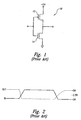
- an inverter 10 is formed by a PMOS transistor 12 and an NMOS transistor 14 coupled in series between a supply voltage V CC , which is typically about 3 volts, and ground potential.
- V CC supply voltage
- the PMOS transistor 12 is turned ON and the NMOS transistor 14 is turned OFF, thereby producing a high, i.e., V CC level, output signal OUT.
- V CC level i.e., V CC level
- the PMOS transistor 12 is turned OFF and the NMOS transistor 14 is turned ON, thereby producing a low, i.e ., ground potential, output.
- one of the transistors 12, 14 is fabricated differently from the other of the transistors 12, 14.
- the channel of one transistor 12, 14 may be fabricated with a channel that is wider or longer than the channel of the other one of the transistors 12, 14, the doping concentrations of the transistors 12, 14 may be different, or the transition voltage V T of the transistors 12, 14 may be different.
- the NMOS transistor 14 has a channel that is wider than the channel of the PMOS transistor 14.
- the NMOS transistor 14 has a smaller resistance than the PMOS transistor 12 with the same gate-to-source voltage V GS .
- the switching characteristics of the inverter 10 are shown in Figure 2, using a voltage level of V CC equal to 3 volts, although other levels ofVCC may be used.
- V CC voltage level of V CC
- the NMOS transistor 14 has a lower resistance than the PMOS transistor 12 because of its increased channel width. Consequently, the output signal OUT has already transitioned to ground potential. The output signal OUT has thus switched from high to low before the input signal IN has switched from low to high.
- the inverter 10 accelerates the input signal IN because the falling edge of the output signal OUT occurs before the rising edge of the input signal IN.
- skewed inverters inherently accelerate one edge of a digital signal only at the expense of delaying the other edge of the digital signal. It is therefore apparent that skewed inverters alone cannot be used to accelerate digital signals in integrated circuits, such as memory devices.
- US 4 985 643 is directed to a speed enhancement technique for CMOS circuits, particularly within a clock pulse generator circuit. Pulses are used to set a logic node to an active state, then some other pulse generated downstream in the circuit is used to reset the node to the inactive state in preparation for the next active pulse.
- a data path includes inverters accelerating a transition from a first logic level to a second logic level, which inverters alternate with inverters accelerating a second transition from the second logic level to the first logic level.
- US 5 929 680 A wherein the preamble of claims 1 and 10 are based discloses a short circuit reduced CMOS buffer circuit with multiple inverter stages for delaying the input signal to reduce short circuit current in the output stage.
- Two signal paths are each composed of two inverters which differ in their channel widths to length ratios. This causes a difference in delay of signal propagation between the two parallel signal paths, so that a signal appearing on a first output node encompasses the signal on a second output node, which output nodes are connected to respective inputs of output transistors.
- the invention is directed to a high speed propagation circuit according to claim 1, and to a method of designating the validity of a digital signal according to claim 10.
- a high speed signal path includes a first plurality of inverters skewed toward a first polarity of signal transition alternating with a second plurality of inverters skewed toward a second polarity of signal transition.
- each of the inverters in the first set accelerates a transition from a first logic level to a second logic level
- each of the inverters in the second set accelerates a transition from the second logic level to the first logic level.
- a pass gate preferably couples an input terminal to the first inverter in the series responsive to a control signal having a first value.
- a preset circuit presets the inverters to a logic level so that any subsequent transition of the inverters resulting from coupling a digital signal through the inverters will be accelerated.
- a pair of the high speed signal paths may be used to couple a digital signal and a clock signal to respective output terminals.
- the high speed signal path for the digital signal With greater skew than the high speed signal path for the clock signal, the digital signal will be present at its output terminal for a period that encompasses the period that the clock signal is present at its output terminal.
- the clock signal can be used to designate a data valid period for the digital signal.
- the high speed signal path may be used in memory devices or other integrated circuits, and a memory device using one or more of the high speed signal paths may be used in a computer system.
- the circuit 20 includes a plurality of address/control signal paths 22, 24, 26 and a clock signal path 40.
- Each of the address/control paths 22, 24, 26 is driven by a respective buffer 44 through a respective pass gate 46.
- the pass gates 46 and the clock signal path 40 are driven by a pulse generator circuit 50 directly and though an inverter 54.
- the pulse generator circuit 50 generates a clock pulse CLKp on each rising edge of an internal clock signal CLK_INT.
- the CLKp signal is also coupled to a clock input of the buffers 44 to clock respective address or control signals out of the buffers 44.
- the pulse generator circuit 50 includes a buffer that receives the internal clock signal CLK_INT and outputs a corresponding CLKIN signal.
- the CLKIN signal is applied to a pass gate 60, to an inverter 62 receiving the CLKIN signal through a conventional time delay circuit 64, and to a NAND gate 70.
- the NAND gate 70 also receives the output of the inverter 62 through an inverter 66.
- the output of the NAND gate 70 is high.
- the high at the output of the NAND gate 70 and a low at the output of an inverter 72 that is coupled to the output of the NAND gate 70 enable the pass gate 60.
- the low CLKIN signal is coupled to the output of the pulse generator 50 to produce a low CLKp signal.
- the low at the output of the NAND gate 70 causes the inverter 72 to output a high, thereby turning ON an NMOS transistor 78.
- the NMOS transistor 78 then couples the CLKp signal to ground.
- a high CLKp pulse is generated on each rising edge of the CLKIN signal for a duration determined by the delay of the time delay circuit 66, as shown in Figure 5.
- the falling edge of the CLKIN signal causes the NAND gate 70 to output a high, again enabling the pass gate 60 and turning OFF the NMOS transistor 78.
- the CLKIN signal is then coupled through the pass gate 60.
- the CLKp signal from the pulse generator 50 therefore remains low until the next rising edge of the CLKIN signal, when another CLKp pulse is generated, as explained above.
- the signal path 22 includes a series of resistors 90 representing the distributed parasitic resistance and capacitance of a signal line.
- a first series of inverters 94 alternating with a second series of inverters 96 are placed at spaced apart locations in the signal line represented by the resistances 90. All of the inverters 94, 96 include a PMOS transistor (not shown) and an NMOS transistor (not shown) in the same configuration of the inverter 10 shown in Figure 1.
- the NMOS transistors of the inverters 94 in the first series have a channel width that is greater than the channel width of the PMOS transistors in the inverters 94.
- the inverters 94 accelerate the rising edge and delay the falling edge of a digital signal applied to their respective inputs.
- the PMOS transistors of the inverters 96 in the second series have a channel width that is greater than the channel width of the NMOS transistors in the inverters 96.
- the inverters 96 accelerate the falling edge and delay the rising edge of a digital signal applied to their respective inputs.
- the signal path 22 greatly accelerates the rising edge of the pulsed input signal and greatly delays the falling edge of the pulsed input signal.
- a rising edge on the CLKp signal out of pulse generator 50 is used to latch an input signal out of input buffer 44, which is coupled to transmission gate 46.
- the high level of CLKp also enables the transmission gate 46 to pass the latched input signal to the input of the first inverter 94 of signal path 22.
- the transmission gate 46 transitions low, the transmission gate 46 is disabled, and a signal path reset device 98 is turned on.
- a high pulse is generated at the input of the signal path 22 if the input to buffer 44 is high when CLKp transitions high. If the input to buffer 44 is low when the CLKp signal transitions high, then the input to the first inverter 94 is signal path 22 will remain low for that clock cycle. Thus, a high pulse input signal is generated only for high inputs, and the default signal level is the low reset level which is preasserted by the reset device 98 prior to the CLKp signal high transition.
- the default low state is guaranteed to have enough time to propagate through the transmission line 22.
- the CLKp signal when the CLKp signal is high to enable the pass gate 46, the low at the output of the inverter 54 turns OFF the NMOS transistor 98 so that the output of the buffer 44 can be applied to the first inverter 94 in the signal path 22.
- the CLKp signal when the CLKp signal is low to disable the pass gate 46, the high at the output of the inverter 54 turns ON the transistor 98 so that the transistor 98 grounds the input to the first inverter 94 in the signal path 22.
- the inputs to all of the inverters 94 are preset to a low logic level, and the inputs to all of the inverters 96 are preset to a high logic level. Presetting the inverters 94, 96 to these logic levels has several effects.
- the inputs to all of the inverters 94, 96 are set to a logic level that causes them to transition with a polarity that will be accelerated by each of the inverters 94, 96. More particularly, the input to each of the inverters 94 is preset low so that, if the logic level of the signal from the buffer 44 causes the inverters 94, 96 to switch logic levels, their inputs will switch from low to high, which is the transition that is accelerated by the inverters 94.
- the input to each of the inverters 96 is preset high so that, if the logic level of the signal from the buffer 44 causes the inverters 94, 96 to switch logic levels, their inputs will switch from high to low, which is the transition that is accelerated by the inverters 96.
- the NMOS transistor 98 presets all of the inverters 94, 96 to a logic level from which a subsequent transition will be accelerated.
- Another advantage to presetting the inverters 94, 96 as described above is that none of the signals propagating through the signal paths 22-26 have adjacent sections that change logic levels in opposite directions. As mentioned above, the propagation delay of signals are increased if adjacent signals are transitioning in opposite directions. As a result of presetting the inputs to the inverters 94, 96, only some of the signal paths 22-26 will be switched. For example, if a signal applied to the path 24 by the buffer 44 is high, all of the inverters 94, 96 in the signal path 24 will be switched. If the respective signals applied to the paths 22, 26 by the respective buffer 44 are low, none of the inverters 94, 96 in the signal paths 22, 26 will be switched.
- the magnitude of the acceleration provided by the inverters 94, 96 is a function of the number of inverters 94, 96 used in the signal path 22.
- the propagation delay of the signal path 22 is proportional to the product of the capacitance and resistance of the signal path 22, both of which are directly proportional to its length.
- the output of the transmission path 22 is either low for a low input, or a high pulse for a high input, however, the high pulse output is wider than the high pulse input.
- the address, command and data signals which are active for both high and low states can be designed to have valid pulse widths that are both accelerated more, and stretched more than the clock signal.
- the signal paths 22-26 are used in a memory device that uses a clock signal to define a data valid window of an address, data or control signal. In such cases, it is important to ensure that a Clock Load signal at the output of the clock signal path 40 is within the time that valid data is present at the outputs of the signal paths 22-26. If the Clock Load signal straddles the time that valid data are present at the outputs of the signal paths 22-26, spurious data may be registered by memory circuits (not shown in Figure 3) that are coupled to the outputs of the signal paths 22-26.
- the inverters 94, 96 in the clock signal path 40 are designed so they have less skew than the inverters 94, 96 in the other signal paths 22-26.
- the clock signal path 40 delays the leading edge of the CLKp signal to a greater extent than the other signal paths 22-26 delay the leading edges of the respective digital signals coupled through those paths 22-25.
- the clock signal path 40 delays the trailing edge of the CLKp signal to a lesser extent than the other signal paths 22-26 delay the trailing edges of the respective digital signals coupled through those paths 22-25.
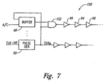
- FIG. 7 An alternative embodiment of a high speed propagation circuit 150 according to another embodiment of the invention is shown in Figure 7.
- the circuit 150 includes most of the same components used in the high speed signal propagation circuit 20 of Figure 3 in the same arrangement.
- the circuit 150 differs from the circuit 20 by substituting a NAND gate 152 for the pass gates 46 and NMOS transistor 98 used in the high speed propagation circuit 20 of Figure 3.
- the NAND gate 152 holds the input to the inverter 98 low to perform the same function performed by the transistor 98 in the circuit 20.
- the NAND gate 152 is enabled to act as an inverter to perform the same function performed by the first inverter 96 in the circuit 20.
- the first inverter 96 in the series that is used in the circuit 20 is not needed.
- the high speed propagation circuit 150 is shown as being implemented with a NAND gate 152, it will be understood that other circuits, such as a NOR gate (not shown) may be used as long as the polarities of the signals applied to the gate are appropriately adjusted.
- the memory device 100 is a synchronous dynamic random access memory (SDRAM) device that includes as its central memory element left and right banks of memory arrays 111A and 11B.
- SDRAM synchronous dynamic random access memory
- Each of the memory arrays 111A and 111B includes a plurality of memory cells (not shown) arranged in rows and columns.
- a control logic circuit 112 controls the data transfer steps associated with a read or write access to the memory cells in the arrays 111A and 111B.
- each of the arrays 111A and 111B has memory cells arranged in 512 rows by 256 columns by 32 bits.
- the memory device 110 has a width of 32 bits - meaning that each memory address (combined bank, row and column address) corresponds to a respective 32-bit memory cell in one of the arrays 111A and 111B, and a processor (not shown in Figure 8) operates on data elements of 32 bits each.
- a processor not shown in Figure 8
- the memory device 100 may have a wide variety of other configurations.
- a system clock (not shown) provides a CLK signal to the control circuit 112 of the memory device 10.
- Command signals are provided to the control circuit 112 and decoded by command decode circuitry 114. These signals are well known in the art, and include signals such as CKE (clock enable), CS (chip select), WE (write enable), RAS (row address strobe) and CAS (column address strobe). Distinct combinations of the various command signals constitute distinct processor commands. For example, the combination of CS low, WE high, RAS low and CAS high can represent an ACTIVE command. Examples of other well-known commands include READ, WRITE, NOP and PRECHARGE. Although the processor actually produces distinct command signals that in combination are registered and decoded as commands by the memory device 110, it is convenient to refer to these commands as being issued by the processor.
- the control logic circuit 112 sends the internal clock CLK_INT signal as well as various control signals on control lines 113 to other parts of the memory device 100, corresponding to the processor-issued command. These control signals may control not only accesses to the memory cells in arrays 111A and 111B, but also a variety of other functions including the input of data to and output of data from the memory device 100.
- the length of the control lines 113 on which the control signal is routed may be fairly long, and they may be spaced close to each other. Consequently, the high speed signal propagation circuit 20a may be used to accelerate the coupling of control signals to various memory components, as shown in Figure 8.
- the memory device 100 is also provided with an address of the memory location to be accessed on a 10-bit wide address bus 115, including a bank address specified by address bit BA and a row or column address specified by address bits A0-A8.
- the address is input to an address register 116 which provides the address information to the control circuit 112, a row-address multiplexer 117, and a column-address latch and decode circuit 120.
- the row-address multiplexer 117 In response to one or more control signals provided by the control circuit 112, the row-address multiplexer 117 multiplexes row address information and provides it to one of two row-address latch and decode circuits 118a and 118b corresponding to the respective memory banks 111a and 111b to be accessed. In response to one or more control signals provided by the control circuit 112, each of the row latch and decode circuits 118a and 118b takes a row address provided by the row-address multiplexer 117 and activates a selected row of memory cells (not shown) in the memory array 111 a and 111 b by selecting one of several row access lines 122a and 122b, respectively.
- the lines coupling the row address multiplexer 117 to the row latch and decode circuits 118a,b may be fairly long and close together, thus reducing the propagation speed of address signals coupled through the lines.
- High speed signal propagation circuits 20b,c may therefore be used to accelerate the coupling of these address signals from the row address multiplexer 117 to the row latch and decode circuits 118a,b.
- the column latch and decode circuit 120 takes a column address provided by the address register 116 and selects one of several column access lines 124a and 124b, each of which is coupled to one of the memory arrays 111 a and 111 b by one of two I/O interface circuits 126a and 126b, respectively.
- each of the I/O interface circuits 126a and 126b selects the 32 memory cells corresponding to the column location in an activated row.
- the lines from the row address multiplexer 117 to the column latch & decode circuits may be long and/or close together. For this reason, the column address signals may be routed from address register 116 to the column latch & decode circuit 120 through a high speed signal propagation circuit 20d of the type shown in Figure 3.
- the I/O interface circuits 126a and 126b include sense amplifiers (not shown) which determine and amplify the logic state of the selected memory cells coupled to the sense amplifiers thorough respective pairs of complimentary digit lines (not shown).
- the I/O interface circuits 126a and 126b also include I/O circuits that gate data to 32 data output registers 128 and from a data input register 130, responsive to one or more control signals provided by the control circuit 112.
- Normally included in the I/O interface circuits 126a,b are DC sense amplifiers (not shown) that receive data from the digit line sense amplifiers and couple the data to the data out register 128.
- the data registers 128 and 130 are connected to a 32-bit wide data bus 31 at DQ pads DQ0-DQ31 to transfer output data Q0-Q31 to a processor and input data D0-D31 from a processor, responsive to one or more control signals provided by the control circuit 112.
- data having a greater or lesser number of bits may alternatively be coupled to or from the memory device 100.
- the memory device 110 includes a refresh control circuit 132 which, responsive to one or more control signals provided by the control circuit 112, initiates regular and periodic activation of each of the rows of the memory cells in the arrays 111a and 111b for purposes of data refresh, as is well known in the art.
- a respective one of the I/O interface circuits A and B senses data stored in the memory cells of the refresh-activated row and rewrites values corresponding to the stored data in each of the memory cells.
- high speed signal propagation circuits 20a-e have been shown in the memory device 100 at specific locations, it will be understood that a fewer or greater number of high speed signal propagation circuits 20 may be used. Also, such high speed signal propagation circuits 20 may be used at different locations or in different types of memory devices or other digital circuits.
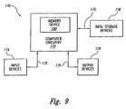
- Figure 9 is a block diagram of one embodiment of a computer system 170 using the memory device 100 of Figure 8.
- the computer system 170 includes computer circuitry 172 for performing such computer functions as executing software to perform desired calculations and tasks.
- Circuitry 172 typically contains a processor (not shown) and the memory device 100 as shown.
- One or more input devices 174 such as a keyboard or a pointing device, is coupled to the computer circuitry 72 via a bus 175 and allows an operator (not shown) to manually input data thereto.
- One or more output devices 176 is coupled to the computer circuitry 172 via the bus 175 to provide to the operator data generated by the circuitry. Examples of output devices 176 include a printer and a video display unit.
- One or more data storage devices 178 is coupled to the computer circuitry 172 via the bus 175 to store data on or retrieve data from external storage media (not shown). Examples of storage devices 178 and associated storage media include drives that accept hard and floppy disks, magnetic tape recorders, and compact-disc read only memory (CD-ROM) readers.
- CD-ROM compact-disc read only memory
Landscapes
- Microelectronics & Electronic Packaging (AREA)
- Engineering & Computer Science (AREA)
- Dram (AREA)
- Static Random-Access Memory (AREA)
- Logic Circuits (AREA)
- Electronic Switches (AREA)
- Semiconductor Integrated Circuits (AREA)
- Radar Systems Or Details Thereof (AREA)
- Burglar Alarm Systems (AREA)
- Stabilization Of Oscillater, Synchronisation, Frequency Synthesizers (AREA)
- Communication Control (AREA)
- Reduction Or Emphasis Of Bandwidth Of Signals (AREA)
- Stereo-Broadcasting Methods (AREA)
Claims (12)
- Hochgeschwindigkeits-Signalausbreitungsschaltung, umfassend:eine Steuerschaltung, aufgebaut zum abwechselnden Erzeugen eines ersten und eines zweiten Werts eines Steuersignals;einen ersten Hochgeschwindigkeits-Datenweg (22) mit einer Mehrzahl von Negatoren (94), die zwischen einem Eingangsknoten und einem Ausgangsknoten in Reihe zueinander geschaltet sind, einer Mehrzahl von Negatoren (96), die in Richtung einer ersten Polarität versetzt sind und abwechseln mit einer Mehrzahl von Negatoren (94), die in Richtung einer zweiten, von der ersten Polarität verschiedenen Polarität versetzt sind, wobei der erste Hochgeschwindigkeits-Datenweg außerdem eine Logikschaltung (44, 46, 98) aufweist, die im Betrieb einen Eingangssignalanschluss mit dem Ausgangsknoten ansprechend auf den ersten Wert des Steuersignals koppelt, der erste Hochgeschwindigkeits-Datenweg außerdem eine erste Voreinstellschaltung aufweist, die im Betrieb ein Eingangssignal eines der Negatoren auf einen logischen Pegel voreinstellt, welcher einer Spannung entspricht, gegenüber der der Negator versetzt ist, um einen Übergang zu beschleunigen, und wobei das Eingangssignal ansprechend auf den zweiten Wert des Steuersignals voreingestellt wird; undeinen zweiten Hochgeschwindigkeits-Datenweg (40) mit einer Mehrzahl von Negatoren (94), die in Reihe zueinander zwischen einem Eingangsknoten und einem Ausgangsknoten liegen, einer Mehrzahl von Negatoren (96), die in Richtung der ersten Polarität versetzt sind und sich abwechseln mit einer Mehrzahl der Negatoren (94), die in Richtung der zweiten Polarität versetzt sind, wobei der zweite Hochgeschwindigkeits-Datenweg außerdem eine zweite Logikschaltung aufweist, die im Betrieb ein Ausgangssignal eines Impulsgenerators (5) mit dem Eingangsknoten ansprechend auf den ersten Wert des Steuersignals koppelt, der zweite Hochgeschwindigkeits-Datenweg außerdem eine zweite Voreinstellschaltung aufweist, die im Betrieb eine Eingangsgröße eines der Negatoren auf einen logischen Pegel voreinstellt, der einer Spannung entspricht, gegenüber der der Negator versetzt ist, um einen Übergang zu beschleunigen, und der Eingang ansprechend auf den zweiten Wert des Steuersignals voreingestellt wird, dadurch gekennzeichnet, dass die Negatoren in dem zweiten Hochgeschwindigkeits-Datenweg kollektiv in einem geringeren Ausmaß versetzt sind, als es die Negatoren in dem ersten Hochgeschwindigkeits-Signalweg kollektiv sind, so dass ein an den Eingangssignalanschluss des ersten Hochgeschwindigkeits-Datenwegs angelegtes Signal an den Ausgangsknoten des ersten Hochgeschwindigkeits-Datenwegs für eine Zeitspanne gekoppelt wird, die eine Zeitspanne beinhaltet, in der ein an den Eingangssignalanschluss des zweiten Hochgeschwindigkeits-Datenwegs angelegtes Signal zu dem Ausgangsknoten des zweiten Hochgeschwindigkeits-Datenwegs gekoppelt wird.
- Schaltung nach Anspruch 1, bei der die erste und die zweite Voreinstellschaltung jeweils einen Schalter aufweisen, der einen Eingang eines der Negatoren mit einer Referenzspannung koppelt, ansprechend auf den zweiten Wert des Steuersignals, wobei die Referenzspannung eine Spannung ist, die dem logischen Pegel entspricht, aus welchem der Negator einen Übergang beschleunigt.
- Schaltung nach Anspruch 2, bei der jeder der Schalter mit dem Eingangsknoten des zugehörigen Hochgeschwindigkeits-Datenwegs gekoppelt ist.
- Schaltung nach Anspruch 1, bei der die Logikschaltung ein Durchlassgatter aufweist.
- Schaltung nach Anspruch 4, bei der das Steuersignal bei einem ersten logischen Pegel besitzt, um das Durchlassgatter zu veranlassen, den Eingangsanschluss mit dem Eingangsknoten zu koppeln, und einen zweiten logischen Pegel hat, um das Durchlassgatter zu veranlassen, den Eingang eines der Negatoren mit einer Referenzspannung zu koppeln, wobei der erste logische Pegel verschieden ist von dem zweiten logischen Pegel.
- Schaltung nach Anspruch 1, bei der die Logikschaltungen und die Voreinstellschaltungen Logikgatter umfassen.
- Schaltung nach Anspruch 1, bei der die Logikschaltung einen Impulsgenerator aufweist, aufgebaut zum Erzeugen des ersten Werts des Steuersignals in Abhängigkeit einer vorbestimmten Flanke eines Taktsignals für eine Dauer, die wesentlich kürzer ist als die Dauer des Taktsignals, wobei der Impulsgenerator den zweiten Wert des Steuersignals immer dann erzeugt, wenn der erste Wert des Steuersignals nicht erzeugt wird.
- Schaltung nach Anspruch 1, bei dem die Logikschaltungen jeweils aufweisen:ein Durchlassgatter, welches den Eingangssignalanschluss mit dem Eingangsknoten verbindet und im Betrieb den Eingangssignalanschluss mit dem Eingangsknoten ansprechend auf den ersten Wert des Steuersignals koppelt; undein Schalter, der einen Eingang eines der Negatoren ansprechend auf einen zweiten Wert des Steuersignals mit einer Referenzspannung koppelt, wobei der zweite Wert des Steuersignals verschieden ist vom ersten Wert des Steuersignals, und die Referenzspannung eine Spannung ist, die dem logischen Pegel entspricht, von dem aus der Negator einen Übergang beschleunigt.
- Schaltung nach Anspruch 8, bei dem der Schalter mit dem Eingangsknoten gekoppelt ist.
- Verfahren zum Kennzeichnen der Gültigkeit eines digitalen Signals, umfassend:Koppeln des digitalen Signals durch eine erste Reihe von Negatoren, die abwechseln zwischen Negatoren, die einen ersten Übergang des digitalen Signals beschleunigen und einen zweiten Übergang des digitalen Signals verzögern, und Negatoren, die den zweiten Übergang des digitalen Signals beschleunigen und den ersten Übergang des digitalen Signals verzögern;Koppel eines Taktsignals durch eine zweite Reihe von Negatoren, die abwechseln zwischen Negatoren, die den ersten Übergang des digitalen Signals beschleunigen und den zweiten Übergang des digitalen Signals verzögern, und Negatoren, die den zweiten Übergang des digitalen Signals beschleunigen und den ersten Übergang des digitalen Signals verzögern, gekennzeichnet durch die Bereitstellung der Übergänge des Taktsignals als Kollektiv auf ein geringeres Maß verzögert und beschleunigt, als die Übergänge des digitalen Signals kollektiv beschleunigt bzw. verzögert werden; undKennzeichnen des digitalen Signals am Ausgang der ersten Reihe von Negatoren als zulässig, wenn das Taktsignal von der zweiten Reihe von Negatoren ausgegeben wird.
- Verfahren nach Anspruch 10, weiterhin umfassend das Voreinstellen der Negatoren in der ersten und der zweiten Reihe auf einen logischen Pegel, von dem aus sie ein Übergang in beschleunigter Weise vollziehen, bevor das digitale Signal und das Taktsignal durch die erste und die zweite Reihe von Negatoren gekoppelt werden.
- Verfahren nach Anspruch 11, weiterhin umfassend das Trennen der Negatoren in der ersten und der zweiten Reihe von dem digitalen Signal und dem Taktsignal, wenn die Negatoren in der ersten und der zweiten Reihe voreingestellt werden.
Applications Claiming Priority (3)
| Application Number | Priority Date | Filing Date | Title |
|---|---|---|---|
| US777835 | 1991-10-11 | ||
| US09/777,835 US6552953B2 (en) | 2001-02-05 | 2001-02-05 | High speed signal path and method |
| PCT/US2002/003342 WO2002063629A1 (en) | 2001-02-05 | 2002-02-04 | High speed signal path and method |
Publications (3)
| Publication Number | Publication Date |
|---|---|
| EP1366495A1 EP1366495A1 (de) | 2003-12-03 |
| EP1366495A4 EP1366495A4 (de) | 2006-03-22 |
| EP1366495B1 true EP1366495B1 (de) | 2007-07-18 |
Family
ID=25111450
Family Applications (1)
| Application Number | Title | Priority Date | Filing Date |
|---|---|---|---|
| EP02706147A Expired - Lifetime EP1366495B1 (de) | 2001-02-05 | 2002-02-04 | Schneller signalweg und verfahren |
Country Status (8)
| Country | Link |
|---|---|
| US (1) | US6552953B2 (de) |
| EP (1) | EP1366495B1 (de) |
| JP (1) | JP4247520B2 (de) |
| KR (1) | KR100854937B1 (de) |
| CN (1) | CN100347784C (de) |
| AT (1) | ATE367637T1 (de) |
| DE (1) | DE60221230T2 (de) |
| WO (1) | WO2002063629A1 (de) |
Families Citing this family (9)
| Publication number | Priority date | Publication date | Assignee | Title |
|---|---|---|---|---|
| US6535038B2 (en) | 2001-03-09 | 2003-03-18 | Micron Technology, Inc. | Reduced jitter clock generator circuit and method for applying properly phased clock signals to clocked devices |
| JP2002313079A (ja) * | 2001-04-18 | 2002-10-25 | Seiko Epson Corp | 半導体メモリ装置の電源ノイズの抑制化 |
| US6628139B2 (en) * | 2001-08-03 | 2003-09-30 | Micron Technology, Inc. | Digital logic devices with extremely skewed trip points and reset circuitry for rapidly propagating signal edges |
| US6738301B2 (en) * | 2002-08-29 | 2004-05-18 | Micron Technology, Inc. | Method and system for accelerating coupling of digital signals |
| US6847582B2 (en) * | 2003-03-11 | 2005-01-25 | Micron Technology, Inc. | Low skew clock input buffer and method |
| US20130076424A1 (en) * | 2011-09-23 | 2013-03-28 | Qualcomm Incorporated | System and method for reducing cross coupling effects |
| US10283187B2 (en) * | 2017-07-19 | 2019-05-07 | Micron Technology, Inc. | Apparatuses and methods for providing additional drive to multilevel signals representing data |
| JP6974549B1 (ja) * | 2020-07-17 | 2021-12-01 | 華邦電子股▲ふん▼有限公司Winbond Electronics Corp. | メモリ装置およびその入出力バッファ制御方法 |
| JP2024048776A (ja) * | 2022-09-28 | 2024-04-09 | ラピステクノロジー株式会社 | データ受信回路、表示ドライバ及び表示装置 |
Family Cites Families (6)
| Publication number | Priority date | Publication date | Assignee | Title |
|---|---|---|---|---|
| US4985643A (en) * | 1988-06-24 | 1991-01-15 | National Semiconductor Corporation | Speed enhancement technique for CMOS circuits |
| US5519344A (en) * | 1994-06-30 | 1996-05-21 | Proebsting; Robert J. | Fast propagation technique in CMOS integrated circuits |
| US5929680A (en) * | 1997-05-16 | 1999-07-27 | Tritech Microelectronics International Ltd | Short circuit reduced CMOS buffer circuit |
| US5999481A (en) * | 1997-08-22 | 1999-12-07 | Micron Technology, Inc. | Method and apparatus for controlling the operation of an integrated circuit responsive to out-of-synchronism control signals |
| US6137849A (en) | 1998-09-09 | 2000-10-24 | Agilent Technologies | System and method for communicating data over a high-speed bus |
| US6331793B1 (en) | 1999-12-30 | 2001-12-18 | Intel Corporation | Apparatus, method and system for pulse passgate topologies |
-
2001
- 2001-02-05 US US09/777,835 patent/US6552953B2/en not_active Expired - Lifetime
-
2002
- 2002-02-04 KR KR1020037010334A patent/KR100854937B1/ko not_active Expired - Lifetime
- 2002-02-04 EP EP02706147A patent/EP1366495B1/de not_active Expired - Lifetime
- 2002-02-04 DE DE60221230T patent/DE60221230T2/de not_active Expired - Lifetime
- 2002-02-04 AT AT02706147T patent/ATE367637T1/de not_active IP Right Cessation
- 2002-02-04 CN CNB028045564A patent/CN100347784C/zh not_active Expired - Lifetime
- 2002-02-04 JP JP2002563485A patent/JP4247520B2/ja not_active Expired - Lifetime
- 2002-02-04 WO PCT/US2002/003342 patent/WO2002063629A1/en not_active Ceased
Non-Patent Citations (1)
| Title |
|---|
| None * |
Also Published As
| Publication number | Publication date |
|---|---|
| US6552953B2 (en) | 2003-04-22 |
| EP1366495A1 (de) | 2003-12-03 |
| DE60221230T2 (de) | 2008-04-17 |
| CN100347784C (zh) | 2007-11-07 |
| ATE367637T1 (de) | 2007-08-15 |
| DE60221230D1 (de) | 2007-08-30 |
| EP1366495A4 (de) | 2006-03-22 |
| JP2004526351A (ja) | 2004-08-26 |
| CN1491416A (zh) | 2004-04-21 |
| JP4247520B2 (ja) | 2009-04-02 |
| KR20030077607A (ko) | 2003-10-01 |
| WO2002063629A1 (en) | 2002-08-15 |
| KR100854937B1 (ko) | 2008-08-29 |
| US20020122346A1 (en) | 2002-09-05 |
Similar Documents
| Publication | Publication Date | Title |
|---|---|---|
| US6105106A (en) | Computer system, memory device and shift register including a balanced switching circuit with series connected transfer gates which are selectively clocked for fast switching times | |
| US6847582B2 (en) | Low skew clock input buffer and method | |
| US6178133B1 (en) | Method and system for accessing rows in multiple memory banks within an integrated circuit | |
| US6317369B1 (en) | Semiconductor device allowing higher speed data transmission to and from external unit | |
| US4760290A (en) | Synchronous logic array circuit with dummy signal lines for controlling "AND" array output | |
| US5400274A (en) | Memory having looped global data lines for propagation delay matching | |
| US20020169919A1 (en) | Column address path circuit and method for memory devices having a burst access mode | |
| KR100260477B1 (ko) | 낮은 전원공급전압에서 고속동작을 하는 반도체 메모리 장치 및 반도체 액세스 방법 | |
| US6777976B2 (en) | Interface circuit and semiconductor device with the same | |
| KR0155177B1 (ko) | 반도체 메모리의 출력 회로 | |
| US7394707B2 (en) | Programmable data strobe enable architecture for DDR memory applications | |
| US6122220A (en) | Circuits and methods for generating internal signals for integrated circuits by dynamic inversion and resetting | |
| US5812492A (en) | Control signal generation circuit and semiconductor memory device that can correspond to high speed external clock signal | |
| US6414902B2 (en) | Use of setup time to send signal through die | |
| EP1366495B1 (de) | Schneller signalweg und verfahren | |
| US5973993A (en) | Semiconductor memory burst length count determination detector | |
| US6166993A (en) | Synchronous semiconductor memory device | |
| US6456563B1 (en) | Semiconductor memory device that operates in sychronization with a clock signal | |
| US6118730A (en) | Phase comparator with improved comparison precision and synchronous semiconductor memory device employing the same | |
| US6058068A (en) | Write driver with locally generated reset pulse | |
| US6683818B1 (en) | Asynchronous random access memory with power optimizing clock | |
| JPH1064276A (ja) | アドレスデコード回路 | |
| JP3625240B2 (ja) | 半導体記憶装置 | |
| JPH11185471A (ja) | 内部クロック信号生成回路 | |
| JP2001067875A (ja) | 出力回路 |
Legal Events
| Date | Code | Title | Description |
|---|---|---|---|
| PUAI | Public reference made under article 153(3) epc to a published international application that has entered the european phase |
Free format text: ORIGINAL CODE: 0009012 |
|
| 17P | Request for examination filed |
Effective date: 20030904 |
|
| AK | Designated contracting states |
Kind code of ref document: A1 Designated state(s): AT BE CH CY DE DK ES FI FR GB GR IE IT LI LU MC NL PT SE TR |
|
| AX | Request for extension of the european patent |
Extension state: AL LT LV MK RO SI |
|
| A4 | Supplementary search report drawn up and despatched |
Effective date: 20060208 |
|
| RIC1 | Information provided on ipc code assigned before grant |
Ipc: H04L 7/00 20060101ALI20060202BHEP Ipc: G11C 8/00 20060101AFI20020819BHEP Ipc: G11C 7/22 20060101ALI20060202BHEP Ipc: G11C 7/10 20060101ALI20060202BHEP |
|
| GRAP | Despatch of communication of intention to grant a patent |
Free format text: ORIGINAL CODE: EPIDOSNIGR1 |
|
| GRAS | Grant fee paid |
Free format text: ORIGINAL CODE: EPIDOSNIGR3 |
|
| GRAA | (expected) grant |
Free format text: ORIGINAL CODE: 0009210 |
|
| AK | Designated contracting states |
Kind code of ref document: B1 Designated state(s): AT BE CH CY DE DK ES FI FR GB GR IE IT LI LU MC NL PT SE TR |
|
| REG | Reference to a national code |
Ref country code: GB Ref legal event code: FG4D |
|
| REG | Reference to a national code |
Ref country code: CH Ref legal event code: EP |
|
| REF | Corresponds to: |
Ref document number: 60221230 Country of ref document: DE Date of ref document: 20070830 Kind code of ref document: P |
|
| REG | Reference to a national code |
Ref country code: IE Ref legal event code: FG4D |
|
| ET | Fr: translation filed | ||
| PG25 | Lapsed in a contracting state [announced via postgrant information from national office to epo] |
Ref country code: PT Free format text: LAPSE BECAUSE OF FAILURE TO SUBMIT A TRANSLATION OF THE DESCRIPTION OR TO PAY THE FEE WITHIN THE PRESCRIBED TIME-LIMIT Effective date: 20071218 Ref country code: FI Free format text: LAPSE BECAUSE OF FAILURE TO SUBMIT A TRANSLATION OF THE DESCRIPTION OR TO PAY THE FEE WITHIN THE PRESCRIBED TIME-LIMIT Effective date: 20070718 Ref country code: ES Free format text: LAPSE BECAUSE OF FAILURE TO SUBMIT A TRANSLATION OF THE DESCRIPTION OR TO PAY THE FEE WITHIN THE PRESCRIBED TIME-LIMIT Effective date: 20071029 Ref country code: NL Free format text: LAPSE BECAUSE OF FAILURE TO SUBMIT A TRANSLATION OF THE DESCRIPTION OR TO PAY THE FEE WITHIN THE PRESCRIBED TIME-LIMIT Effective date: 20070718 |
|
| REG | Reference to a national code |
Ref country code: CH Ref legal event code: PL |
|
| NLV1 | Nl: lapsed or annulled due to failure to fulfill the requirements of art. 29p and 29m of the patents act | ||
| PG25 | Lapsed in a contracting state [announced via postgrant information from national office to epo] |
Ref country code: LI Free format text: LAPSE BECAUSE OF FAILURE TO SUBMIT A TRANSLATION OF THE DESCRIPTION OR TO PAY THE FEE WITHIN THE PRESCRIBED TIME-LIMIT Effective date: 20070718 Ref country code: AT Free format text: LAPSE BECAUSE OF FAILURE TO SUBMIT A TRANSLATION OF THE DESCRIPTION OR TO PAY THE FEE WITHIN THE PRESCRIBED TIME-LIMIT Effective date: 20070718 Ref country code: CH Free format text: LAPSE BECAUSE OF FAILURE TO SUBMIT A TRANSLATION OF THE DESCRIPTION OR TO PAY THE FEE WITHIN THE PRESCRIBED TIME-LIMIT Effective date: 20070718 |
|
| PG25 | Lapsed in a contracting state [announced via postgrant information from national office to epo] |
Ref country code: BE Free format text: LAPSE BECAUSE OF FAILURE TO SUBMIT A TRANSLATION OF THE DESCRIPTION OR TO PAY THE FEE WITHIN THE PRESCRIBED TIME-LIMIT Effective date: 20070718 |
|
| PG25 | Lapsed in a contracting state [announced via postgrant information from national office to epo] |
Ref country code: DK Free format text: LAPSE BECAUSE OF FAILURE TO SUBMIT A TRANSLATION OF THE DESCRIPTION OR TO PAY THE FEE WITHIN THE PRESCRIBED TIME-LIMIT Effective date: 20070718 Ref country code: GR Free format text: LAPSE BECAUSE OF FAILURE TO SUBMIT A TRANSLATION OF THE DESCRIPTION OR TO PAY THE FEE WITHIN THE PRESCRIBED TIME-LIMIT Effective date: 20071019 |
|
| PLBE | No opposition filed within time limit |
Free format text: ORIGINAL CODE: 0009261 |
|
| STAA | Information on the status of an ep patent application or granted ep patent |
Free format text: STATUS: NO OPPOSITION FILED WITHIN TIME LIMIT |
|
| 26N | No opposition filed |
Effective date: 20080421 |
|
| PG25 | Lapsed in a contracting state [announced via postgrant information from national office to epo] |
Ref country code: SE Free format text: LAPSE BECAUSE OF FAILURE TO SUBMIT A TRANSLATION OF THE DESCRIPTION OR TO PAY THE FEE WITHIN THE PRESCRIBED TIME-LIMIT Effective date: 20071018 |
|
| PG25 | Lapsed in a contracting state [announced via postgrant information from national office to epo] |
Ref country code: MC Free format text: LAPSE BECAUSE OF NON-PAYMENT OF DUE FEES Effective date: 20080228 |
|
| PG25 | Lapsed in a contracting state [announced via postgrant information from national office to epo] |
Ref country code: IE Free format text: LAPSE BECAUSE OF NON-PAYMENT OF DUE FEES Effective date: 20080204 |
|
| PG25 | Lapsed in a contracting state [announced via postgrant information from national office to epo] |
Ref country code: CY Free format text: LAPSE BECAUSE OF FAILURE TO SUBMIT A TRANSLATION OF THE DESCRIPTION OR TO PAY THE FEE WITHIN THE PRESCRIBED TIME-LIMIT Effective date: 20070718 |
|
| PG25 | Lapsed in a contracting state [announced via postgrant information from national office to epo] |
Ref country code: LU Free format text: LAPSE BECAUSE OF NON-PAYMENT OF DUE FEES Effective date: 20080204 |
|
| PG25 | Lapsed in a contracting state [announced via postgrant information from national office to epo] |
Ref country code: TR Free format text: LAPSE BECAUSE OF FAILURE TO SUBMIT A TRANSLATION OF THE DESCRIPTION OR TO PAY THE FEE WITHIN THE PRESCRIBED TIME-LIMIT Effective date: 20070718 |
|
| PGFP | Annual fee paid to national office [announced via postgrant information from national office to epo] |
Ref country code: GB Payment date: 20130130 Year of fee payment: 12 |
|
| GBPC | Gb: european patent ceased through non-payment of renewal fee |
Effective date: 20140204 |
|
| PG25 | Lapsed in a contracting state [announced via postgrant information from national office to epo] |
Ref country code: GB Free format text: LAPSE BECAUSE OF NON-PAYMENT OF DUE FEES Effective date: 20140204 |
|
| REG | Reference to a national code |
Ref country code: FR Ref legal event code: PLFP Year of fee payment: 15 |
|
| REG | Reference to a national code |
Ref country code: FR Ref legal event code: PLFP Year of fee payment: 16 |
|
| REG | Reference to a national code |
Ref country code: DE Ref legal event code: R082 Ref document number: 60221230 Country of ref document: DE Representative=s name: SCHMITT-NILSON SCHRAUD WAIBEL WOHLFROM PATENTA, DE |
|
| REG | Reference to a national code |
Ref country code: FR Ref legal event code: PLFP Year of fee payment: 17 |
|
| PGFP | Annual fee paid to national office [announced via postgrant information from national office to epo] |
Ref country code: FR Payment date: 20210223 Year of fee payment: 20 Ref country code: IT Payment date: 20210223 Year of fee payment: 20 |
|
| PGFP | Annual fee paid to national office [announced via postgrant information from national office to epo] |
Ref country code: DE Payment date: 20210329 Year of fee payment: 20 |