EP1360711B1 - Halbleiteranordnung und verfahren zur ätzung einer schicht der halbleiteranordnung mittels einer siliziumhaltigen ätzmaske - Google Patents
Halbleiteranordnung und verfahren zur ätzung einer schicht der halbleiteranordnung mittels einer siliziumhaltigen ätzmaske Download PDFInfo
- Publication number
- EP1360711B1 EP1360711B1 EP02700152A EP02700152A EP1360711B1 EP 1360711 B1 EP1360711 B1 EP 1360711B1 EP 02700152 A EP02700152 A EP 02700152A EP 02700152 A EP02700152 A EP 02700152A EP 1360711 B1 EP1360711 B1 EP 1360711B1
- Authority
- EP
- European Patent Office
- Prior art keywords
- layer
- etching
- mask
- silicon
- mask layer
- Prior art date
- Legal status (The legal status is an assumption and is not a legal conclusion. Google has not performed a legal analysis and makes no representation as to the accuracy of the status listed.)
- Expired - Lifetime
Links
Images
Classifications
-
- H—ELECTRICITY
- H01—ELECTRIC ELEMENTS
- H01L—SEMICONDUCTOR DEVICES NOT COVERED BY CLASS H10
- H01L21/00—Processes or apparatus adapted for the manufacture or treatment of semiconductor or solid state devices or of parts thereof
- H01L21/02—Manufacture or treatment of semiconductor devices or of parts thereof
- H01L21/04—Manufacture or treatment of semiconductor devices or of parts thereof the devices having potential barriers, e.g. a PN junction, depletion layer or carrier concentration layer
- H01L21/18—Manufacture or treatment of semiconductor devices or of parts thereof the devices having potential barriers, e.g. a PN junction, depletion layer or carrier concentration layer the devices having semiconductor bodies comprising elements of Group IV of the Periodic Table or AIIIBV compounds with or without impurities, e.g. doping materials
- H01L21/30—Treatment of semiconductor bodies using processes or apparatus not provided for in groups H01L21/20 - H01L21/26
- H01L21/31—Treatment of semiconductor bodies using processes or apparatus not provided for in groups H01L21/20 - H01L21/26 to form insulating layers thereon, e.g. for masking or by using photolithographic techniques; After treatment of these layers; Selection of materials for these layers
- H01L21/32—Treatment of semiconductor bodies using processes or apparatus not provided for in groups H01L21/20 - H01L21/26 to form insulating layers thereon, e.g. for masking or by using photolithographic techniques; After treatment of these layers; Selection of materials for these layers using masks
-
- H—ELECTRICITY
- H01—ELECTRIC ELEMENTS
- H01L—SEMICONDUCTOR DEVICES NOT COVERED BY CLASS H10
- H01L21/00—Processes or apparatus adapted for the manufacture or treatment of semiconductor or solid state devices or of parts thereof
- H01L21/02—Manufacture or treatment of semiconductor devices or of parts thereof
- H01L21/027—Making masks on semiconductor bodies for further photolithographic processing not provided for in group H01L21/18 or H01L21/34
- H01L21/033—Making masks on semiconductor bodies for further photolithographic processing not provided for in group H01L21/18 or H01L21/34 comprising inorganic layers
- H01L21/0332—Making masks on semiconductor bodies for further photolithographic processing not provided for in group H01L21/18 or H01L21/34 comprising inorganic layers characterised by their composition, e.g. multilayer masks, materials
-
- H—ELECTRICITY
- H01—ELECTRIC ELEMENTS
- H01L—SEMICONDUCTOR DEVICES NOT COVERED BY CLASS H10
- H01L21/00—Processes or apparatus adapted for the manufacture or treatment of semiconductor or solid state devices or of parts thereof
- H01L21/02—Manufacture or treatment of semiconductor devices or of parts thereof
- H01L21/027—Making masks on semiconductor bodies for further photolithographic processing not provided for in group H01L21/18 or H01L21/34
- H01L21/033—Making masks on semiconductor bodies for further photolithographic processing not provided for in group H01L21/18 or H01L21/34 comprising inorganic layers
- H01L21/0334—Making masks on semiconductor bodies for further photolithographic processing not provided for in group H01L21/18 or H01L21/34 comprising inorganic layers characterised by their size, orientation, disposition, behaviour, shape, in horizontal or vertical plane
- H01L21/0335—Making masks on semiconductor bodies for further photolithographic processing not provided for in group H01L21/18 or H01L21/34 comprising inorganic layers characterised by their size, orientation, disposition, behaviour, shape, in horizontal or vertical plane characterised by their behaviour during the process, e.g. soluble masks, redeposited masks
-
- H—ELECTRICITY
- H01—ELECTRIC ELEMENTS
- H01L—SEMICONDUCTOR DEVICES NOT COVERED BY CLASS H10
- H01L21/00—Processes or apparatus adapted for the manufacture or treatment of semiconductor or solid state devices or of parts thereof
- H01L21/02—Manufacture or treatment of semiconductor devices or of parts thereof
- H01L21/04—Manufacture or treatment of semiconductor devices or of parts thereof the devices having potential barriers, e.g. a PN junction, depletion layer or carrier concentration layer
- H01L21/18—Manufacture or treatment of semiconductor devices or of parts thereof the devices having potential barriers, e.g. a PN junction, depletion layer or carrier concentration layer the devices having semiconductor bodies comprising elements of Group IV of the Periodic Table or AIIIBV compounds with or without impurities, e.g. doping materials
- H01L21/30—Treatment of semiconductor bodies using processes or apparatus not provided for in groups H01L21/20 - H01L21/26
- H01L21/31—Treatment of semiconductor bodies using processes or apparatus not provided for in groups H01L21/20 - H01L21/26 to form insulating layers thereon, e.g. for masking or by using photolithographic techniques; After treatment of these layers; Selection of materials for these layers
- H01L21/3105—After-treatment
- H01L21/311—Etching the insulating layers by chemical or physical means
- H01L21/31105—Etching inorganic layers
- H01L21/31111—Etching inorganic layers by chemical means
- H01L21/31116—Etching inorganic layers by chemical means by dry-etching
-
- H—ELECTRICITY
- H01—ELECTRIC ELEMENTS
- H01L—SEMICONDUCTOR DEVICES NOT COVERED BY CLASS H10
- H01L21/00—Processes or apparatus adapted for the manufacture or treatment of semiconductor or solid state devices or of parts thereof
- H01L21/02—Manufacture or treatment of semiconductor devices or of parts thereof
- H01L21/04—Manufacture or treatment of semiconductor devices or of parts thereof the devices having potential barriers, e.g. a PN junction, depletion layer or carrier concentration layer
- H01L21/18—Manufacture or treatment of semiconductor devices or of parts thereof the devices having potential barriers, e.g. a PN junction, depletion layer or carrier concentration layer the devices having semiconductor bodies comprising elements of Group IV of the Periodic Table or AIIIBV compounds with or without impurities, e.g. doping materials
- H01L21/30—Treatment of semiconductor bodies using processes or apparatus not provided for in groups H01L21/20 - H01L21/26
- H01L21/31—Treatment of semiconductor bodies using processes or apparatus not provided for in groups H01L21/20 - H01L21/26 to form insulating layers thereon, e.g. for masking or by using photolithographic techniques; After treatment of these layers; Selection of materials for these layers
- H01L21/3105—After-treatment
- H01L21/311—Etching the insulating layers by chemical or physical means
- H01L21/31144—Etching the insulating layers by chemical or physical means using masks
Definitions
- the present application relates to a semiconductor device and a method for etching a layer of the semiconductor device by means of a silicon-containing etching mask.
- etching processes are used to pattern semiconductor substrates.
- an etching mask is applied to a layer to be structured and patterned by photolithography. Some areas of the layer to be patterned are now covered and protected by the etch mask, whereas other areas of the layer to be etched are exposed.
- the layer to be etched is removed by means of an etchant. In this case, the areas of the layer to be etched covered by the etching mask are protected from the etching substance, so that no etching is carried out on the layer to be etched at these positions. Since both the layer to be etched and the etching mask are exposed to the etching substance in the etching process, both layers are removed.
- an etching mask having a high selectivity to the layer to be etched using the etchant is selected. This means that the etching removal at the etching mask is substantially lower than the etching removal at the layer to be etched. This makes it possible to etch deep structures into the layer to be etched with relatively thin etching masks.
- Typical materials used in silicon semiconductor technology are silicon, silicon oxide and silicon nitride. With a suitable etching substance, each of the three materials is suitable for being used as an etching mask for one or both of the other materials.
- an etching mask made of silicon is suitable for etching silicon oxide or silicon nitride in conjunction with a fluorohydrocarbon-containing etching gas.
- a semiconductor device comprising a semiconductor substrate having a substrate surface on which is disposed a layer comprising silicon oxide or silicon nitride having a surface with a silicon-containing mask layer disposed on the surface of the layer to act as the layer To serve etching mask, wherein the mask layer additionally contains a sulfur- or carbon-containing substance, wherein the sulfur is present in a sulfur-hydrogen compound or the carbon in a hydrocarbon chain, whereby the etch resistance of the mask layer is increased.
- the additional substance serves as an additive in the mask layer, whereby the etching rate of the silicon-containing mask layer is reduced.
- deeper trenches may be etched into a layer to be etched with a thinner mask layer.
- An embodiment of the invention provides that the substance forms a proportion of up to 50% of the mask layer.
- the substance forms a solid at a pressure between 0.13 and 67 Pa and a temperature between -20 ° C and 200 ° C and a gaseous substance as oxidized and / or nitrided molecule.
- This has the advantage that the substance in the specified temperature range can be integrated as a solid substance in the mask layer and on the other hand can be converted by means of oxygen in a gaseous and thus volatile form, so that the additional substance during the etching process can be transported away.
- the silicon-containing etching mask is formed almost of silicon and the layer of silicon oxide to be etched, the silicon oxide is converted into silicon fluoride and oxygen by means of a fluorocarbon-containing etching gas.
- the silicon-containing mask layer is attacked and converted to a much lesser extent by the etching substance. This is further reduced by the additional substance.
- the additional substance is now likewise arranged in the vicinity of or on the silicon oxide layer to be etched, the additional substance is oxidized by the oxygen released from the silicon oxide layer and converted into a volatile gaseous form. As a result, the etching selectivity between the silicon-containing etching mask and the silicon oxide layer to be etched is increased.
- the invention provides that the substance contains carbon in the form of a hydrocarbon chain or sulfur in the form of hydrogen sulfide. Carbon and sulfur are advantageously suitable for reducing the removal rate of carbon- or sulfur-added silicon in a fluorohydrocarbon-containing etching gas.
- an embodiment of the invention provides that the substance contains aluminum, gallium, indium, thallium or boron in a concentration with more than 10 19 atoms per cm 3 and is electrically activated. Electrical activated means that boron is bound to lattice sites of the Si crystal lattice.
- the substances mentioned are p-dopants for the silicon-containing mask layer.
- a p-doped mask layer also has an increased etch resistance.
- the layer to be etched contains silicon oxide or silicon nitride.
- a further embodiment of the invention provides that the substance is implanted in the silicon-containing mask layer.
- a further embodiment of the invention provides that the substance is incorporated by means of supply during the formation of the silicon-containing mask layer in the silicon-containing mask layer.
- the inventive method leads carbon and / or sulfur together with an etching gas in an etching system, whereby the etching rate of the silicon-containing etching mask is reduced.
- An embodiment of the method according to the invention provides that the hydrocarbon molecules contained in the etching gas, which contain, for example, CH 4 , and / or sulfur-hydrogen compound containing, for example, SH 2 , are enriched in or on the mask layer during the etching step.
- the enrichment in or on the mask layer has the advantage that the etch resistance of the silicon-containing etching mask is increased and thus its etch rate is reduced.
- a further advantageous method step provides that the carbon and / or sulfur atoms contained in the etching gas are enriched in or on the mask layer during the etching step.
- the accumulation of carbon and / or sulfur atoms also has the advantage that the etching rate of the silicon-containing mask layer is reduced.
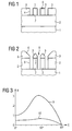
- FIG. 1 shows a substrate 1 on which a layer 2 is arranged.
- the layer 2 has a surface 7 which faces away from the substrate 1.
- a mask layer 3 is arranged on the surface 7 of the layer 2.
- the mask layer 3 is formed to have a mask pattern 4 as a trench in the mask layer 3.
- the substrate 1 consists for example of a silicon-containing material.
- the layer 2 contains silicon oxide and / or silicon nitride.
- the mask layer 3 contains silicon, wherein the silicon content can be up to 100%.
- a first variant provides that an additional substance 8 is contained in the silicon-containing mask layer 3.
- the additional substance is, for example, carbon and / or sulfur.
- the additional substance is deposited, for example, during the formation of the mask layer 3 together with the mask layer 3, whereby the substance 8 is incorporated in the mask layer 3.
- a further variant of the method for forming the mask layer 3 initially forms the mask layer 3 without the additional substance 8. Subsequently, the additional substance 8 is introduced into the mask layer 3, for example by means of an implantation.
- p-type dopants such as aluminum, gallium, indium, thallium and boron are suitable.
- the layer 2 is etched in accordance with the arrangement shown in Figure 2.
- FIG 2 the arrangement shown in Figure 1 is shown at a later time.
- an etching has been carried out with a fluorohydrocarbon-containing etching gas, wherein a trench 5 has been formed in the layer 2 and a facet 6 has been formed on the mask layer 3.
- the substance 8 on the one hand, causes the removal rate of the mask layer 2 to be reduced, and in particular causes the removal rate to be reduced at the facet angle that forms. In this case, the facet angle between the substrate surface and the facet 6 is measured.
- a further exemplary embodiment according to FIG. 1 initially forms the mask layer 3 without the additional substance 8.
- the additional substance 8 is admixed with the etching gas and causes the etching selectivity to increase in the course of the etching process, since the additional substance 8 enters into and / or enriched at the mask layer 3.
- the removal rate of the mask layer 3 is thereby reduced.
- the substance 8 accumulates in the mask layer 3, whereby the ⁇ tzselektology is further increased.
- the layer 2 has a thickness of 1000 nm and is formed of silicon oxide and / or silicon nitride.
- the mask layer 3 can be formed, for example, with a thickness of 100 nm of silicon and additionally comprises the substance 8.
- the additional substance 8 causes the removal rate of the mask layer 3 to be reduced and, in particular, the removal rate at the forming facet angle is lowered.
- FIG. 3 shows a diagram which reproduces on the horizontal axis, designated E, the angle of incidence E of the etching substance on the substrate in degrees (°).
- E the angle of incidence
- R the etching rate - normalized to an angle of incidence of 0 ° - is plotted.
- a first curve 9 represents, for example, the etching rate of an amorphous silicon layer.
- the normalized removal rate is 1. The removal rate increases for angles between 40 ° and 45 ° to a maximum of approximately 3 and decreases for larger angles until at an angle of incidence of 90 °, a removal rate of 0 is reached.
- the etching substance penetrates perpendicular to a patterned amorphous silicon layer, a particularly rapid etching removal takes place in the direction of a 40 ° to 45 ° angle, resulting in a so-called taper, which forms the facet 6.
- the second curve 10 is also normalized to the removal rate of the first curve 9 at an angle of incidence of 0 °. Due to the additional substance 8, the etching rate is reduced to a fraction of the etching rate without additional substance. For larger angles, the ⁇ tzabtragsrate increases to about 1.5 times at an angle of 55 °. This means that the additional substance 8 results in a much weaker taper effect, as a result of which the facet 6 is formed with a steeper angle and a reduced removal rate.
Landscapes
- Engineering & Computer Science (AREA)
- Computer Hardware Design (AREA)
- Physics & Mathematics (AREA)
- Condensed Matter Physics & Semiconductors (AREA)
- General Physics & Mathematics (AREA)
- Manufacturing & Machinery (AREA)
- Microelectronics & Electronic Packaging (AREA)
- Power Engineering (AREA)
- Chemical & Material Sciences (AREA)
- Inorganic Chemistry (AREA)
- General Chemical & Material Sciences (AREA)
- Chemical Kinetics & Catalysis (AREA)
- Drying Of Semiconductors (AREA)
Applications Claiming Priority (3)
| Application Number | Priority Date | Filing Date | Title |
|---|---|---|---|
| DE10103524 | 2001-01-26 | ||
| DE10103524A DE10103524A1 (de) | 2001-01-26 | 2001-01-26 | Verfahren und Halbleiteranordnung zur Ätzung einer Schicht eines Halbleitersubstrats mittels einer siliziumhaltigen Ätzmaske |
| PCT/DE2002/000130 WO2002059951A1 (de) | 2001-01-26 | 2002-01-17 | Halbleiteranordnung und verfahren zur ätzung einer schicht der halbleiteranordnung mittels einer siliziumhaltigen ätzmaske |
Publications (2)
| Publication Number | Publication Date |
|---|---|
| EP1360711A1 EP1360711A1 (de) | 2003-11-12 |
| EP1360711B1 true EP1360711B1 (de) | 2007-03-14 |
Family
ID=7671843
Family Applications (1)
| Application Number | Title | Priority Date | Filing Date |
|---|---|---|---|
| EP02700152A Expired - Lifetime EP1360711B1 (de) | 2001-01-26 | 2002-01-17 | Halbleiteranordnung und verfahren zur ätzung einer schicht der halbleiteranordnung mittels einer siliziumhaltigen ätzmaske |
Country Status (7)
| Country | Link |
|---|---|
| US (1) | US6864188B2 (enExample) |
| EP (1) | EP1360711B1 (enExample) |
| JP (1) | JP2004517505A (enExample) |
| KR (1) | KR100516839B1 (enExample) |
| DE (2) | DE10103524A1 (enExample) |
| TW (1) | TW548743B (enExample) |
| WO (1) | WO2002059951A1 (enExample) |
Families Citing this family (4)
| Publication number | Priority date | Publication date | Assignee | Title |
|---|---|---|---|---|
| US7553770B2 (en) | 2007-06-06 | 2009-06-30 | Micron Technology, Inc. | Reverse masking profile improvements in high aspect ratio etch |
| KR101972159B1 (ko) | 2012-08-24 | 2019-08-16 | 에스케이하이닉스 주식회사 | 실리콘함유하드마스크를 구비한 반도체장치 및 그 제조 방법 |
| KR102051529B1 (ko) | 2013-03-25 | 2020-01-08 | 에스케이하이닉스 주식회사 | 반도체 장치 및 그 제조방법, 그리고 반도체 장치를 포함하는 마이크로프로세서, 프로세서, 시스템, 데이터 저장 시스템 및 메모리 시스템 |
| CN111584358A (zh) * | 2020-04-09 | 2020-08-25 | 中国科学院微电子研究所 | 刻蚀沟槽的方法 |
Family Cites Families (26)
| Publication number | Priority date | Publication date | Assignee | Title |
|---|---|---|---|---|
| GB1147014A (en) * | 1967-01-27 | 1969-04-02 | Westinghouse Electric Corp | Improvements in diffusion masking |
| DE2557079C2 (de) * | 1975-12-18 | 1984-05-24 | Ibm Deutschland Gmbh, 7000 Stuttgart | Verfahren zum Herstellen einer Maskierungsschicht |
| JPS5351970A (en) * | 1976-10-21 | 1978-05-11 | Toshiba Corp | Manufacture for semiconductor substrate |
| US4211601A (en) * | 1978-07-31 | 1980-07-08 | Bell Telephone Laboratories, Incorporated | Device fabrication by plasma etching |
| US4283249A (en) * | 1979-05-02 | 1981-08-11 | International Business Machines Corporation | Reactive ion etching |
| US5362682A (en) * | 1980-04-10 | 1994-11-08 | Massachusetts Institute Of Technology | Method of producing sheets of crystalline material and devices made therefrom |
| NL8301262A (nl) * | 1983-04-11 | 1984-11-01 | Philips Nv | Werkwijze voor het vervaardigen van een halfgeleiderinrichting, waarbij met behulp van ionenimplantatie patronen worden aangebracht in een laag siliciumnitride. |
| JPS62224687A (ja) * | 1986-03-25 | 1987-10-02 | Anelva Corp | エツチング方法 |
| US5091047A (en) * | 1986-09-11 | 1992-02-25 | National Semiconductor Corp. | Plasma etching using a bilayer mask |
| FR2610140B1 (fr) * | 1987-01-26 | 1990-04-20 | Commissariat Energie Atomique | Circuit integre cmos et procede de fabrication de ses zones d'isolation electrique |
| US4782009A (en) * | 1987-04-03 | 1988-11-01 | General Electric Company | Method of coating and imaging photopatternable silicone polyamic acid |
| FR2652448B1 (fr) * | 1989-09-28 | 1994-04-29 | Commissariat Energie Atomique | Procede de fabrication d'un circuit integre mis haute tension. |
| JP3006048B2 (ja) * | 1990-07-27 | 2000-02-07 | ソニー株式会社 | ドライエッチング方法 |
| US5240554A (en) * | 1991-01-22 | 1993-08-31 | Kabushiki Kaisha Toshiba | Method of manufacturing semiconductor device |
| US5217568A (en) * | 1992-02-03 | 1993-06-08 | Motorola, Inc. | Silicon etching process using polymeric mask, for example, to form V-groove for an optical fiber coupling |
| JP3111661B2 (ja) * | 1992-07-24 | 2000-11-27 | ソニー株式会社 | ドライエッチング方法 |
| US5350484A (en) * | 1992-09-08 | 1994-09-27 | Intel Corporation | Method for the anisotropic etching of metal films in the fabrication of interconnects |
| US5525535A (en) * | 1995-07-26 | 1996-06-11 | United Microelectronics Corporation | Method for making doped well and field regions on semiconductor substrates for field effect transistors using liquid phase deposition of oxides |
| JPH1160735A (ja) * | 1996-12-09 | 1999-03-05 | Toshiba Corp | ポリシランおよびパターン形成方法 |
| TW505984B (en) * | 1997-12-12 | 2002-10-11 | Applied Materials Inc | Method of etching patterned layers useful as masking during subsequent etching or for damascene structures |
| US6025273A (en) * | 1998-04-06 | 2000-02-15 | Taiwan Semiconductor Manufacturing Company, Ltd. | Method for etching reliable small contact holes with improved profiles for semiconductor integrated circuits using a carbon doped hard mask |
| US6387819B1 (en) * | 1998-04-29 | 2002-05-14 | Applied Materials, Inc. | Method for etching low K dielectric layers |
| JP2001210726A (ja) * | 2000-01-24 | 2001-08-03 | Hitachi Ltd | 半導体装置及びその製造方法 |
| US6527968B1 (en) * | 2000-03-27 | 2003-03-04 | Applied Materials Inc. | Two-stage self-cleaning silicon etch process |
| KR20030007904A (ko) * | 2000-06-06 | 2003-01-23 | 이케이씨 테크놀로지, 인코포레이티드 | 전자 재료 제조 방법 |
| US6583046B1 (en) * | 2001-07-13 | 2003-06-24 | Advanced Micro Devices, Inc. | Post-treatment of low-k dielectric for prevention of photoresist poisoning |
-
2001
- 2001-01-26 DE DE10103524A patent/DE10103524A1/de not_active Ceased
-
2002
- 2002-01-17 EP EP02700152A patent/EP1360711B1/de not_active Expired - Lifetime
- 2002-01-17 WO PCT/DE2002/000130 patent/WO2002059951A1/de not_active Ceased
- 2002-01-17 KR KR10-2003-7009879A patent/KR100516839B1/ko not_active Expired - Fee Related
- 2002-01-17 JP JP2002560183A patent/JP2004517505A/ja active Pending
- 2002-01-17 DE DE50209714T patent/DE50209714D1/de not_active Expired - Fee Related
- 2002-01-21 TW TW091100879A patent/TW548743B/zh not_active IP Right Cessation
-
2003
- 2003-06-04 US US10/454,518 patent/US6864188B2/en not_active Expired - Lifetime
Also Published As
| Publication number | Publication date |
|---|---|
| US6864188B2 (en) | 2005-03-08 |
| KR20030074745A (ko) | 2003-09-19 |
| DE50209714D1 (de) | 2007-04-26 |
| JP2004517505A (ja) | 2004-06-10 |
| WO2002059951A1 (de) | 2002-08-01 |
| TW548743B (en) | 2003-08-21 |
| KR100516839B1 (ko) | 2005-09-26 |
| DE10103524A1 (de) | 2002-08-22 |
| US20030207588A1 (en) | 2003-11-06 |
| EP1360711A1 (de) | 2003-11-12 |
Similar Documents
| Publication | Publication Date | Title |
|---|---|---|
| EP1444724B1 (de) | Photolithographisches strukturierungsverfahren mit einer durch ein plasmaverfahren abgeschiedenen kohlenstoff-hartmaskenschicht mit diamantartiger härte | |
| EP0098318B1 (de) | Verfahren zum Herstellen von Gräben mit im wesentlichen vertikalen Seitenwänden in Silicium durch reaktives Ionenätzen | |
| DE19680590B4 (de) | Verfahren zur Herstellung von Beschleunigungssensoren | |
| DE2812658C3 (de) | Verfahren zum selektiven Diffundieren von Aluminium in ein Einkristall-Siliciumhalbleitersubstrat | |
| EP1014434A1 (de) | Verfahren zum anisotropen plasmachemischen Trockenätzen von Siliziumnitrid-Schichten mittels eines Fluor enthaltenden Gasgemisches | |
| DE1614999B2 (de) | Verfahren zum herstellen einer maskierungsschicht aus dielektrischem material | |
| DE3135815A1 (de) | "verfahren zur herstellung integrierter schaltungen" | |
| DE2930293A1 (de) | Aetzverfahren bei der herstellung eines gegenstandes | |
| DE3618128A1 (de) | Verfahren zur herstellung eines mos-kondensators | |
| EP0094528A2 (de) | Verfahren zum Herstellen von Strukturen von aus Metallsilizid und Polysilizium bestehenden Doppelschichten auf integrierte Halbleiterschaltungen enthaltenden Substraten durch reaktives Ionenätzen | |
| DE3317222A1 (de) | Verfahren zum herstellen einer halbleiterstruktur | |
| DE2225374B2 (de) | Verfahren zum herstellen eines mos-feldeffekttransistors | |
| DE2239686A1 (de) | Verfahren zur herstellung von dielektrisch isolierten schichtbereichen aus einem siliciumhalbleitermaterial auf einer traegerschicht | |
| DE19736145B4 (de) | Verfahren zum Planieren von Halbleiterwafern | |
| EP1360711B1 (de) | Halbleiteranordnung und verfahren zur ätzung einer schicht der halbleiteranordnung mittels einer siliziumhaltigen ätzmaske | |
| DE10224137A1 (de) | Ätzgas und Verfahren zum Trockenätzen | |
| DE1814029B2 (de) | Erzeugung einkristalliner und polykristalliner halbleiterbereiche auf einem inkristallinen halbleitersubstrat | |
| EP1294019A1 (de) | Verfahren zum Herstellen einer Halbleiterstruktur unter Verwendung einer Schutzschicht und Halbleiterstruktur | |
| DE10229346A1 (de) | Verfahren zur Herstellung eines Halbleiterelementes | |
| DE10330795A1 (de) | Kohlenstoff-Hartmaske mit haftfähiger Schicht zur Haftung auf Metall | |
| DE10137575A1 (de) | Verfahren zur Erzeugung einer Maske sowie Verfahren zur Herstellung einer Halbleitervorrichtung | |
| DE10231533A1 (de) | Verfahren zur Metallstrukturierung | |
| DE112018003719T5 (de) | Schneideverfahren | |
| DE1614358C3 (de) | Verfahren zum Herstellen einer Ätzmaske für die Ätzbehandlung von Halbleiterkörpern | |
| EP0898733B1 (de) | Verfahren zur herstellung einer stencil-maske |
Legal Events
| Date | Code | Title | Description |
|---|---|---|---|
| PUAI | Public reference made under article 153(3) epc to a published international application that has entered the european phase |
Free format text: ORIGINAL CODE: 0009012 |
|
| 17P | Request for examination filed |
Effective date: 20030717 |
|
| AK | Designated contracting states |
Kind code of ref document: A1 Designated state(s): AT BE CH CY DE DK ES FI FR GB GR IE IT LI LU MC NL PT SE TR |
|
| AX | Request for extension of the european patent |
Extension state: AL LT LV MK RO SI |
|
| GRAP | Despatch of communication of intention to grant a patent |
Free format text: ORIGINAL CODE: EPIDOSNIGR1 |
|
| RBV | Designated contracting states (corrected) |
Designated state(s): DE FR GB IE IT |
|
| GRAS | Grant fee paid |
Free format text: ORIGINAL CODE: EPIDOSNIGR3 |
|
| GRAA | (expected) grant |
Free format text: ORIGINAL CODE: 0009210 |
|
| AK | Designated contracting states |
Kind code of ref document: B1 Designated state(s): DE FR GB IE IT |
|
| PG25 | Lapsed in a contracting state [announced via postgrant information from national office to epo] |
Ref country code: IE Free format text: LAPSE BECAUSE OF FAILURE TO SUBMIT A TRANSLATION OF THE DESCRIPTION OR TO PAY THE FEE WITHIN THE PRESCRIBED TIME-LIMIT Effective date: 20070314 |
|
| REG | Reference to a national code |
Ref country code: GB Ref legal event code: FG4D Free format text: NOT ENGLISH |
|
| REF | Corresponds to: |
Ref document number: 50209714 Country of ref document: DE Date of ref document: 20070426 Kind code of ref document: P |
|
| REG | Reference to a national code |
Ref country code: IE Ref legal event code: FG4D Free format text: LANGUAGE OF EP DOCUMENT: GERMAN |
|
| GBV | Gb: ep patent (uk) treated as always having been void in accordance with gb section 77(7)/1977 [no translation filed] |
Effective date: 20070314 |
|
| REG | Reference to a national code |
Ref country code: IE Ref legal event code: FD4D |
|
| EN | Fr: translation not filed | ||
| EN | Fr: translation not filed | ||
| PG25 | Lapsed in a contracting state [announced via postgrant information from national office to epo] |
Ref country code: GB Free format text: LAPSE BECAUSE OF FAILURE TO SUBMIT A TRANSLATION OF THE DESCRIPTION OR TO PAY THE FEE WITHIN THE PRESCRIBED TIME-LIMIT Effective date: 20070314 |
|
| PLBE | No opposition filed within time limit |
Free format text: ORIGINAL CODE: 0009261 |
|
| STAA | Information on the status of an ep patent application or granted ep patent |
Free format text: STATUS: NO OPPOSITION FILED WITHIN TIME LIMIT |
|
| 26N | No opposition filed |
Effective date: 20071217 |
|
| PG25 | Lapsed in a contracting state [announced via postgrant information from national office to epo] |
Ref country code: IT Free format text: LAPSE BECAUSE OF FAILURE TO SUBMIT A TRANSLATION OF THE DESCRIPTION OR TO PAY THE FEE WITHIN THE PRESCRIBED TIME-LIMIT Effective date: 20070314 Ref country code: FR Free format text: LAPSE BECAUSE OF FAILURE TO SUBMIT A TRANSLATION OF THE DESCRIPTION OR TO PAY THE FEE WITHIN THE PRESCRIBED TIME-LIMIT Effective date: 20071102 |
|
| PGFP | Annual fee paid to national office [announced via postgrant information from national office to epo] |
Ref country code: DE Payment date: 20080315 Year of fee payment: 7 |
|
| PG25 | Lapsed in a contracting state [announced via postgrant information from national office to epo] |
Ref country code: FR Free format text: LAPSE BECAUSE OF FAILURE TO SUBMIT A TRANSLATION OF THE DESCRIPTION OR TO PAY THE FEE WITHIN THE PRESCRIBED TIME-LIMIT Effective date: 20070314 |
|
| PG25 | Lapsed in a contracting state [announced via postgrant information from national office to epo] |
Ref country code: DE Free format text: LAPSE BECAUSE OF NON-PAYMENT OF DUE FEES Effective date: 20090801 |