EP1343266A2 - Dispositif de transmission optique - Google Patents
Dispositif de transmission optique Download PDFInfo
- Publication number
- EP1343266A2 EP1343266A2 EP03100530A EP03100530A EP1343266A2 EP 1343266 A2 EP1343266 A2 EP 1343266A2 EP 03100530 A EP03100530 A EP 03100530A EP 03100530 A EP03100530 A EP 03100530A EP 1343266 A2 EP1343266 A2 EP 1343266A2
- Authority
- EP
- European Patent Office
- Prior art keywords
- optical
- transmission apparatus
- signals
- optical transmission
- signal
- Prior art date
- Legal status (The legal status is an assumption and is not a legal conclusion. Google has not performed a legal analysis and makes no representation as to the accuracy of the status listed.)
- Withdrawn
Links
Images


Classifications
-
- H—ELECTRICITY
- H04—ELECTRIC COMMUNICATION TECHNIQUE
- H04J—MULTIPLEX COMMUNICATION
- H04J14/00—Optical multiplex systems
- H04J14/08—Time-division multiplex systems
Definitions
- the present invention relates to an optical transmission apparatus which multiplexes a plurality of electric signals, converts these signals to an optical signal, and transmits this optical signal.
- the pulse width of an optical signal does not depend on the signal pattern, and the non-linear resistance is high, making it suitable for high-speed optical transmission.
- the CS-RZ (Carrier Suppressed Return-to-Zero) format in which the phase of the light inverts for each bit has been proposed (Japanese Patent Application No. 2000-82997). Because the modulation bandwidth in the CS-RZ format is narrow, it has high dispersion tolerance, and is suitable for dense wavelength division multiplexing transmission.
- FIG. 1 shows a case in which two Mach-Zehnder optical modulators are connected in a cascade manner, wherein by driving one with a clock signal of a frequency B and the other by a data signal of a bit rate B, an RZ format optical signal is generated.
- a continuous light 32 output from a continuous-wave (CW) light source 31 is modulated by a clock signal 39 input into a modulating electrode 36-1 of the first Mach-Zehnder optical modulator 38-1, and modulated into a 01 alternating pulse light.
- the pulse light is then modulated by a data signal 33 input into a modulating electrode 36-2 of the second Mach-Zehnder optical modulator 38-2, thereby generating an RZ format optical signal 37.
- FIG. 2 shows a timing chart of this process.
- a 01 alternating pulse light of a frequency B is generated from the continuous light, and is modulated by the data signal so as to generate RZ format modulated light.
- the continuous light 32 output from the continuous-wave (CW) light source 31 is modulated by a clock signal 40 input into a modulating electrode 36-1 and a clock signal 41 input into a modulating electrode 36-3 in a first push-pull type Mach-Zehnder optical modulator 38-3, and modulated to a 01 alternating pulse light.
- the clock signal 40 and the clock signal 41 have opposite polarity and peak-to-peak amplitude of V ⁇ /2, and the frequency of each signal is B/2.
- the amplitude V ⁇ refers to a voltage magnitude required to invert (shift by ⁇ phases) the phase of the optical signal, and the frequency B is the clock frequency of the data signal 33.
- the light output from the push-pull type Mach-Zehnder optical modulator 38-3 is modulated to a 01 alternating pulse light in which the phase of the optical signal is inverted in each timeslot.
- the modulated pulse light is modulated in the Mach-Zehnder optical modulator 38-2 by the data signal 33 input into the modulating electrode 36-2, thereby generating a 01 alternating optical signal 37 in which the phase of the light is inverted in each bit as shown in FIG. 4.
- a method of accelerating optical transmission using optical time division multiplexing has also been proposed (Japanese Unexamined Patent Application First Publication No. Hei 10-79705). This method is described here with reference to FIG. 5.
- the continuous light 32 output from the continuous wave (CW) light source 31 is divided into N light beams by an optical divider 34, and each portion of the divided continuous light 32 is modulated by a first modulator 30 by means of a clock signal 39 of a frequency B input into the modulating electrode 36, thereby obtaining modulated, 01 alternating pulse lights.
- the pulse lights are modulated in a second modulator 30 by a data signal 33 input into a modulating electrode 39, to obtain optical signals.
- the data signal 33 and the clock signal are delayed by (T/N) x k (where k is an integer from 1 to N-1).
- the optical signals are then combined by an optical combiner 35 to produce an optical signal 37.
- the generated optical signal 37 is a B x N Return-to-zero format optical signal.
- FIG. 6 shows a timing chart of this process.
- the data signals #1 through #4 are converted to the RZ format optical signal in two modulators. After the optical data signal #2 is delayed by 1/4 timeslots, the optical data signal #3 is delayed by 2/4 timeslots, and the optical data signal #4 is delayed by 3/4 timeslots, the optical signals are combined. Thus the combined optical data signal is a multiplexed signal, in the return-to-zero format.
- an optical modulator with an operating bandwidth of B x N is required, but by providing a phase control device which varies the phases of the optical signals in either even numbered or odd numbered channels by an odd multiple of ⁇ when the optical combiner combines the signals, an optical modulator with an operating bandwidth of the bit rate B x N/2 can be used. Because the phase of the light of adjacent bits in the multiplexed signal is inverted, the optical signals cancel each other out in the portions between bits where the pulses overlap. Consequently, it is possible to generate an RZ format optical signal with a bit rate of B ⁇ N using an optical modulator with an operating bandwidth of B x N/2. As a result, an RZ format optical signal in which the phase of the light inverts for each bit is generated. However, because the pulse width differs according to the signal pattern, it is not strictly a CS-RZ format optical signal.
- an object of the present invention is to provide an optical transmission apparatus which can transmit RZ format, NRZ format, alternating phase RZ format, phase modulated NRZ format and CS-RZ format optical signals, using fewer optical modulators than conventional apparatuses.
- a first aspect of the present invention is an optical transmission apparatus in which a plurality of input electrical signals are multiplex modulated onto an optical signal with a frequency A, comprising an interferometer modulator which comprises a plurality of modulating electrodes on one of the arms thereof, a continuous wave light source which supplies an carrier light to the interferometer modulator, devices which convert the plurality of input electrical signals to RZ format signals each with a pulse width of 1/A or less, applies a different delay to each signal, each delay differing sequentially by 1/A, and then inputs the signals to the modulating electrodes of the interferometer modulator, and a device which applies a half wavelength phase difference to the input light of the interferometer modulator, between the two arms of the interferometer modulator.
- a second aspect of the present invention is an optical transmission apparatus in which a plurality of input electrical signals are multiplex modulated onto an optical signal with a bit rate of A, comprising an interferometer modulator which comprises a plurality of modulating electrodes on one of the arms thereof, a continuous wave light source which supplies an carrier light to the interferometer modulator, and devices which convert the plurality of input electrical signals to RZ format signals each with a pulse width of 1 /A or less, and applies a different delay to each signal, each delay differing sequentially by 1/A, and which after inverting the signal polarity of even numbered or odd numbered input electrical signals, inputs the signals to the modulating electrodes of the interferometer modulator.
- a third aspect of the present invention is an optical transmission apparatus in which a plurality of input electrical signals are multiplex modulated onto an optical signal with a bit rate of A, comprising an interferometer modulator which comprises a plurality of modulating electrodes on one of the arms thereof, a pulse light source which supplies a pulse light to the interferometer modulator, and devices which convert the plurality of input electrical signals to RZ format signals each with a pulse width of 1 /A or less, and applies a different delay to each signal, each delay differing sequentially by 1/A, and which after inverting the signal polarity of even numbered or odd numbered input electrical signals, inputs the signals to the modulating electrodes of the interferometer modulator.
- a fourth aspect of the present invention is an optical transmission apparatus in which a plurality of input electrical signals are multiplex modulated onto an optical signal with a bit rate of A, comprising an interferometer modulator which comprises an equal number of modulating electrodes on each arm thereof, a continuous wave light source which supplies an carrier light to the interferometer modulator, devices which convert the plurality of input electrical signals to RZ format signals each with a pulse width of 1/A or less, applies a different delay to each signal, each delay differing sequentially by 1/A, and then inputs the signals to the modulating electrodes of the interferometer modulator, and a device which applies a half wavelength phase difference to the input light of the interferometer modulator, between the two arms of the interferometer modulator.
- a fifth aspect of the present invention is an optical transmission apparatus in which a plurality of input electrical signals are multiplex modulated onto an optical signal with a bit rate of A, comprising an interferometer modulator which comprises an equal number of modulating electrodes on each arm thereof, a pulse light source which supplies a pulse light to the interferometer modulator, devices which convert the plurality of input electrical signals to RZ format signals each with a pulse width of 1/A or less, applies a different delay to each signal, each delay differing sequentially by 1/A, and then inputs the signals to the modulating electrodes of the interferometer modulator, and a device which applies a half wavelength phase difference to the input light of the interferometer modulator, between the two arms of the interferometer modulator.
- a sixth aspect of the present invention is an optical transmission apparatus in which a plurality of input electrical signals are multiplex modulated onto an optical signal with a bit rate of A, comprising an interferometer modulator which comprises an equal number of modulating electrodes on each arm thereof, a continuous wave light source which supplies an carrier light to the interferometer modulator, and devices which convert the plurality of input electrical signals to RZ format signals each with a pulse width of 1 /A or less, and applies a different delay to each signal, each delay differing sequentially by 1/A, and which after inverting the signal polarity of even numbered or odd numbered input electrical signals, inputs the signals to the modulating electrodes of the interferometer modulator.
- a seventh aspect of the present invention is an optical transmission apparatus in which a plurality of input electrical signals are multiplex modulated onto an optical signal with a bit rate of A, comprising an interferometer modulator which comprises an equal number of modulating electrodes on each arm thereof, a pulse light source which supplies a pulse light to the interferometer modulator, and devices which convert the plurality of input electrical signals to RZ format signals each with a pulse width of 1 /A or less, and applies a different delay to each signal, each delay differing sequentially by 1/A, and which after inverting the signal polarity of even numbered or odd numbered input electrical signals, inputs the signals to the modulating electrodes of the interferometer modulator.
- An eighth aspect of the present invention is an optical transmission apparatus in which a plurality of input electrical signals are multiplex modulated onto an optical signal with a bit rate of A, comprising a continuous wave light source which supplies an carrier light, an optical divider which divides the carrier light from the continuous wave light source into N number of carrier lights (where N is an integer), N number of optical modulators which modulate each divided carrier light divided in the optical divider with an electrical signal, an optical combiner which combines the optical signals from the N number of optical modulators, and a device which converts the N input electrical signals to RZ format signals each with a pulse width of 1/A or less, applies a different delay to each signal, each delay differing sequentially by 1/A, and then inputs the signals to the optical modulators.
- a ninth aspect of the present invention is an optical transmission apparatus in which a plurality of input electrical signals are multiplex modulated onto an optical signal with a bit rate of A, comprising a continuous wave light source which supplies an carrier light, an optical divider which divides the carrier light from the continuous wave light source into N number of carrier lights (where N is an integer), N number of optical modulators which modulate each divided carrier light divided in the optical divider with an electrical signal, optical delays which apply a different delay to each signal from the N number of optical modulators, each delay differing sequentially by 1/A, an optical combiner which combines the optical signals from the optical delays, and devices which after converting the N input electrical signals to RZ format signals each with a pulse width of 1/A or less, input the signals to the optical modulators.
- a tenth aspect of the present invention is an optical transmission apparatus in which a plurality of input electrical signals are multiplex modulated onto an optical signal with a bit rate of A, comprising a continuous wave light source which supplies an carrier light, an optical divider which divides the carrier light from the continuous wave light source into N number of carrier lights (where N is an integer), N number of optical modulators which modulate each divided carrier light divided in the optical divider with an electrical signal, optical phase shifters which shift the phase of the light of the optical signals from the N number of optical modulators so as to generate a half period phase difference between even numbered signals and odd numbered signals, an optical combiner which combines the optical signals from the optical phase shifters, and a device which converts the N input electrical signals to RZ format signals each with a pulse width of 1/A or less, applies a different delay to each signal, each delay differing sequentially by 1/A, and then inputs the signals to the optical modulators.
- An eleventh aspect of the present invention is an optical transmission apparatus in which a plurality of input electrical signals are multiplex modulated onto an optical signal with a bit rate of A, comprising a continuous wave light source which supplies an carrier light, an optical divider which divides the carrier light from the continuous wave light source into N number of carrier lights (where N is an integer), N number of optical modulators which modulate each divided carrier light divided in the optical divider with an electrical signal, optical phase shifters which shift the optical phase of either even numbered signals or odd numbered signals received from the N number of optical modulators by an odd multiple of a half period, an optical combiner which combines the optical signals from the optical phase shifters, and a device which converts the N input electrical signals to RZ format signals each with a pulse width of 1/A or less, applies a different delay to each signal, each delay differing sequentially by 1/A, and then inputs the signals to the optical modulators.
- a twelfth aspect of the present invention is an optical transmission apparatus in which a plurality of input electrical signals are multiplex modulated onto an optical signal with a bit rate of A, comprising a continuous wave light source which supplies an carrier light, an optical divider which divides the carrier light from the continuous wave light source into N number of carrier lights (where N is an integer), N number of optical modulators which modulate each divided carrier light divided in the optical divider with an electrical signal, optical delays which apply a different delay to each signal from the N number of optical modulators, each delay differing sequentially by 1/A, optical phase shifters which shift the optical phase of optical signals received from the optical delays so as to generate a difference of a half period between even numbered signals and odd numbered signals, an optical combiner which combines the optical signals from the optical phase shifters, and devices which after converting the N input electrical signals to RZ format signals each with a pulse width of 1/A or less, input the signals to the optical modulators.
- a thirteenth aspect of the present invention is an optical transmission apparatus in which a plurality of input electrical signals are multiplex modulated onto an optical signal with a bit rate of A, comprising a continuous wave light source which supplies an carrier light, an optical divider which divides the carrier light from the continuous wave light source into N number of carrier lights (where N is an integer), N number of optical modulators which modulate each divided carrier light divided in the optical divider with an electrical signal, optical delays which apply a different delay to each signal from the N number of optical modulators, each delay differing sequentially by 1/A, optical phase shifters which shift the optical phase of either even numbered signals or odd numbered signals received from the optical delays by an odd multiple of a half period, an optical combiner which combines the optical signals from the optical phase shifters, and devices which after converting the N input electrical signals to RZ format signals each with a pulse width of 1/A or less, input the signals to the optical modulators.
- This optical transmission apparatus comprises a continuous wave light source 11 which outputs an carrier light, a Mach-Zehnder optical modulator 18 which comprises N (where N is an integer of 2 or greater) modulating electrodes 16-1 to 16-N, N number of RZ converters 14-1 to 14-N which convert NRZ format data signals to an RZ format, delays 15-1 to 15-(N-1) which apply a delay of (1/A) x k to the data signals in each channel from 2 to N, respectively, and a bias circuit 10 which applies a bias of V ⁇ to one of the arms of the Mach-Zehnder optical modulator 18, thereby functioning as a device which applies a half wavelength phase difference to the input light of the interferometer modulator between the two arms of the interferometer modulator.
- N is an integer of 2 or greater
- A is the bit rate of an optical signal 17
- k is an integer between 1 and N-1
- V ⁇ is the drive voltage required to shift the phase of the input light by a half wavelength.
- the bias circuit 10 is provided on the arm where the data signals are modulated, but the bias circuit 10 may also be provided on the opposite arm, and apply a voltage of V ⁇ to this opposite arm. Alternatively, voltages of+V ⁇ /2 and -V ⁇ /2 may be applied to each arm, respectively. Furthermore, the order of connection of the delays 15 and the RZ converters 14 may be changed.
- the carrier light 12 from the continuous wave light source 11 is input into the Mach-Zehnder optical modulator 18.
- a bias of V ⁇ is applied to one arm of the Mach-Zehnder optical modulator 18 by the bias circuit 10.
- the data signals 13 of channels 1 to N are converted by the RZ converters 14-1 to 14-N to RZ format signals, each with a pulse width of 1/A or less, that is a duty of 1/N or less. If the pulse width is 1/A, the resulting optical signal 17 is an NRZ format signal, and if the pulse width is 1/(2A), the resulting optical signal 17 is an RZ format signal with a duty of 50%.
- the applied voltage amplitude may be V ⁇ peak-to-peak.
- the signals are modulated by the modulating electrodes 16-1 to 16-N of the Mach-Zehnder optical modulator 18, thereby generating an optical signal 17 with a bit rate of A.
- there is no delay connected to the modulating electrode 16-1 but a delay may be connected to every modulating electrode in order to apply a delay difference of 1/A to each signal.
- FIG. 8 shows a case in which the signals are converted to RZ (Return-to-Zero) format signals with a pulse width of 1/(2A), that is a duty of 1/(2N), by the RZ converters 14-1 to 14-N.
- RZ Return-to-Zero
- FIG. 9 shows a case in which the signals are converted to RZ (Return-to-Zero) format signals with a pulse width of 1/A, that is a duty of 1/N, by the RZ converters 14-1 to 14-N. Following the same operation as in FIG. 8, the resulting multiplex modulated optical signal is a NRZ format signal with a duty of 100%.
- RZ Return-to-Zero
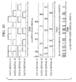
- FIG. 10 A timing chart showing a case in which multiplex modulation of four data signals is performed is shown in FIG. 10.
- data signals each with a bit rate of A/4 are multiplexed.
- modulated light is output with a duty of 50% and a bit rate of A.
- the data signals #3 and #4 are converted to RZ format signals, they are multiplexed in the same manner as the other signals by being blanked at half the frequency of the other signals.
- modulated light is generated in the NRZ format with a bit rate of A and a duty of 100%.
- the optical transmission apparatus described in the present embodiment it was possible to perform multiplex modulation of a plurality of data signals into an RZ format or NRZ format optical signal using fewer Mach-Zehnder optical modulators than in conventional optical transmission apparatuses. As a result, it was also possible to reduce optical loss from the case in which multiplex modulation of the signals was performed with conventional Mach-Zehnder optical modulators in a cascading connection.
- This optical communication apparatus comprises a continuous wave light source 11 which outputs an carrier light, a Mach-Zehnder optical modulator 18 which comprises N (where N is an even number of 2 or greater) modulating electrodes 16-1 to 16-N, N number of RZ converters 14-1 to 14-N which convert NRZ format data signals to RZ format signals, delays 15-1 to 15-(N-1) which apply a delay of (1/A) x k to the data signals in the channels 2 to N, respectively, and signal polarity inverters 19 which invert the polarity of the even numbered data signals.
- A is the bit rate of an optical signal 17
- k is an integer between 1 and N-1.
- the signal polarity inverters 19 were provided for the even numbered data signals, but they may be provided for the odd numbered data signals. Furthermore, the order of connection of the signal polarity inverters 19, the delays 15 and the RZ converters 14 may also be changed.
- An carrier light 12 from the continuous wave light source 11 is input into the Mach-Zehnder optical modulator 18.
- the data signals 13 of channels 1 to N are each converted to RZ (Return-to-Zero) format signals with a pulse width of 1/A or less, that is a duty of 1/N or less, by the RZ converters 14-1 to 14-N. If the pulse width is 1/A, the resulting data signals of the optical signal 17 are RZ format signals with varying duties, and if the pulse width is 1/(2A), the resulting data signals of the optical signal 17 are RZ format signals with a duty of 50%.
- the applied voltage amplitude may be V ⁇ peak-to-peak.
- the signals are modulated by the modulating electrodes 16-1 to 16-N of the Mach-Zehnder optical modulator 18, thereby generating an optical signal 17 with a bit rate of A.
- FIG. 13 shows a case in which the signals are converted to RZ (Return-to-Zero) format signals with a pulse width of 1/(2A), that is a duty of 1/(2N), by the RZ converters 14-1 to 14-N. Because the signal polarity of the even numbered data signals is inverted, when both signals are "0", the phase difference between the arms is ⁇ , and the resulting optical signal is "0".
- RZ Return-to-Zero
- the multiplex modulated optical signal is an alternating phase RZ format signal with a duty of 50%.
- FIG. 14 shows a case in which the signals are converted to RZ (Return-to-Zero) format signals with a pulse width of 1/A, that is a duty of 1/N, by the RZ converters 14-1 to 14-N.
- the resulting multiplex modulated optical signal is a RZ format signal with a duty which varies from 50% to 100% in alternate phases.
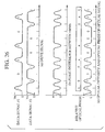
- An eye pattern is shown in FIG. 21. In FIG. 21, the duty varies between 50%, 75% and 100%.
- the optical transmission apparatus described in the present embodiment it was possible to perform multiplex modulation of a plurality of data signals into an alternating phase RZ format optical signal or an alternating phase RZ format optical signal with a varying duty, using fewer Mach-Zehnder optical modulators than in conventional optical transmission apparatuses. As a result, it was also possible to reduce optical loss from the case in which multiplex modulation of the signals was performed with conventional Mach-Zehnder optical modulators in a cascading connection.
- This optical communication apparatus comprises a pulse light source 21 which outputs a pulse light, a Mach-Zehnder optical modulator 18 which comprises N (where N is an even number of 2 or greater) modulating electrodes 16-1 to 16-N, N number of RZ converters 14-1 to 14-N which convert NRZ format data signals to RZ format signals, delays 15-1 to 15-(N-1) which apply a delay of (1/A) x k to the data signals in channels 2 to N, respectively, and signal polarity inverters 19 which invert the polarity of the even numbered data signals.
- A is the bit rate of the optical signal 17
- k is an integer between 1 and N-1.
- the signal polarity inverters 19 were provided for the even numbered data signals, but they may also be provided for the odd numbered data signals instead. Furthermore, the order of connection of the signal polarity inverter 19, the delays 15 and the RZ converters 14 may be changed.
- a pulse light 26 from the pulse light source 21 is input into the Mach-Zehnder optical modulator 18.
- the data signals 13 of channels 1 to N are converted to RZ (Return-to-Zero) format signals with a pulse width of 1/ or less, that is a duty of 1/N or less, by the RZ converters 14-1 to 14-N, respectively.
- RZ Return-to-Zero
- the data signals of the optical signal 17 are NRZ format signals
- the pulse width is 1/(2A)
- the data signals of the optical signal 17 are RZ format signals with a duty of 50%.
- the pulse width is limited to the width of the pulse light supplied by the pulse light source 21.
- the applied voltage amplitude may be V ⁇ peak-to-peak.
- the signals are modulated by the modulating electrodes 16-1 to 16-N, thereby generating an optical signal 17 with a bit rate of A.
- FIG. 16 and FIG. 17 Each figure shows an example in which multiplex modulation of two data signals is performed.
- the principles of the multiplex modulation are substantially the same as in embodiment 2, with the exception that the duty of the pulse is limited to the pulse width of the pulse light source.
- the generated optical signal is a CS-RZ format signal.
- the same CS-RZ format optical signal is output in the examples in both FIG. 16 and FIG. 17.
- the optical transmission apparatus described in the present embodiment it is possible to perform multiplex modulation of a plurality of data signals into a CS-RZ format optical signal using fewer Mach-Zehnder optical modulators than in conventional optical transmission apparatuses. As a result, it was also possible to reduce optical loss from the case in which multiplex modulation of the signals was performed with conventional Mach-Zehnder optical modulators in a cascading connection.
- This optical communication apparatus comprises a continuous wave light source 11 which outputs an carrier light, a push-pull type Mach-Zehnder optical modulator 18 which comprises N (where N is an even number of 2 or greater) modulating electrodes 16-1 to 16-N, N number of RZ converters 14-1 to 14-N which convert NRZ format data signals to RZ format signals, delays 15-1 to 15-(N-1) which apply a delay of (1/A) x k to the data signals of channels 2 to N, respectively, and a bias circuit 10 which applies a bias of V ⁇ to one of the arms of the Mach-Zehnder optical modulator 18.
- the odd numbered data signals are applied to the modulating electrodes provided on one arm of the Mach-Zehnder optical modulator, and the even numbered data signals are applied to the modulating electrodes provided on the other arm of the Mach-Zehnder optical modulator.
- A is the bit rate of the optical signal 17
- k is an integer between 1 and N-1
- V ⁇ is the drive voltage required to shift the phase of the input light by a half wavelength.
- the bias circuit 10 was provided on the arm where modulation of the odd numbered data signals is performed, but it may also be provided on the opposite arm instead. Furthermore, the order of connection of the delays 15 and the RZ converters 14 may be changed.
- An carrier light 12 from the continuous wave light source 11 is input into the Mach-Zehnder optical modulator 18, and a bias of V ⁇ is applied to one of the arms of the Mach-Zehnder optical modulator 18 by the bias circuit 10.
- the data signals 13 of channels 1 to N are each converted to a RZ (Return-to-Zero) format signals with a pulse width of 1/A or less, that is a duty of 1/N or less, by the RZ converters 14-1 to 14-N. If the pulse width is 1/A, the resulting data signals of the optical signal 17 are RZ format signals with varying duties, and if the pulse width is 1/(2A), the resulting data signals of the optical signal 17 are RZ format signals with a duty of 50%.
- the applied voltage amplitude may be V ⁇ peak-to-peak.
- the signals after the signals have been delayed by (1/A) x k by the delays 15-1 to 15-(N-1), respectively, the signals are modulated by the modulating electrodes 16-1 to 16-N, thereby generating an optical signal 17 with a bit rate of A.
- FIG. 19 shows an example in which multiplex modulation of two data signals is performed.
- FIG. 19 shows a case in which the signals are converted to RZ (Return-to-Zero) format signals with a pulse width of 1/(2A) that is a duty of 1/(2N), by the RZ converters 14-1 to 14-N. Because a bias of V ⁇ is applied to one of the arms of the Mach-Zehnder optical modulator 18, when both signals are "0", the phase difference between the arms is ⁇ , and the resulting optical signal is "0".
- RZ Return-to-Zero
- the resulting multiplex modulated optical signal is an alternating phase RZ format signal with a duty of 50%.
- FIG. 20 shows a case in which the signals are converted to RZ (Return-to-Zero) format signals with a pulse width of 1/A, that is a duty of 1/N, by the RZ converters 14-1 to 14-N.
- the resulting multiplex modulated optical signal is an alternating phase RZ format signal with a duty varying from 50% to 100%.
- An eye pattern is shown in FIG. 21. In FIG. 21, the duty varies between 50%, 75% and 100%.
- the optical transmission apparatus described in the present embodiment it was possible to perform multiplex modulation of a plurality of data signals into an alternating phase RZ format optical signal or an alternating phase RZ format optical signal with a varying duty, using fewer Mach-Zehnder optical modulators than in conventional optical transmission apparatuses. As a result, it was also possible to reduce optical loss from the case in which multiplex modulation of the signals was performed with conventional Mach-Zehnder optical modulators in a cascading connection.
- This optical communication apparatus comprises a pulse light source 21 which outputs a pulse light, a Mach-Zehnder optical modulator 18 which comprises N (where N is an even number of 2 or greater) modulating electrodes 16-1 to 16-N, N number of RZ converters 14-1 to 14-N which convert NRZ format data signals to RZ format signals, delays 15-1 to 15-(N-1) which apply a delay of (1/A) x k to the data signals of channels 2 to N, respectively, and a bias circuit 10 which applies a bias of V ⁇ to one of the arms of the Mach-Zehnder optical modulator 18.
- the odd numbered data signals are applied to the modulating electrodes provided on one arm of the Mach-Zehnder optical modulator, and the even numbered data signals are applied to the modulating electrodes provided on the other arm of the Mach-Zehnder optical modulator.
- A is the bit rate of the optical signal 17
- k is an integer between 1 and N-1.
- the bias circuit 10 was provided on the arm where modulation of the odd numbered data signals is performed, but it may also be provided on the opposite arm instead. Furthermore, the order of connection of the delays 15 and the RZ converters 14 may be changed.
- a pulse light 26 from the pulse light source 21 is input into the Mach-Zehnder optical modulator 18.
- the data signals 13 of channels 1 to N are converted to RZ (Return-to-Zero) format signals with a pulse width of 1/A or less, that is a duty of 1/N or less, by the RZ converters 14-1 to 14-N, respectively, and when the pulse width is 1/A, the resulting data signals of the optical signal 17 are RZ format signals with varying duties, and when the pulse width is 1/(2A), the resulting data signals of the optical signal 17 are RZ format signals with a duty of 50%.
- RZ Return-to-Zero
- the pulse width is limited to the width of the pulse light supplied by the pulse light source 21.
- the applied voltage amplitude may be V ⁇ peak-to-peak.
- the signals after the signals have been delayed by (1/A) x k by the delays 15-1 to 15-(N-1), respectively, they are then modulated by the modulating electrodes 16-1 to 16-N, thereby generating an optical signal 17 with a bit rate of A.
- FIG. 23 and FIG. 24 The principles of the multiplex modulation performed in the present optical transmission apparatus are shown in FIG. 23 and FIG. 24. Each figure shows an example in which multiplex modulation of two data signals is performed.
- the principles of the multiplex modulation are substantially the same as in embodiment 4, with the exception that the duty of the pulse is limited to the pulse width of the pulse light source.
- the generated optical signal is a CS-RZ format signal.
- the same CS-RZ format optical signal is output in the examples in both FIG. 23 and FIG. 24.
- the optical transmission apparatus described in the present embodiment it is possible to perform multiplex modulation of a plurality of data signals into a CS-RZ format optical signal using fewer Mach-Zehnder optical modulators than in conventional optical transmission apparatuses. As a result, it was also possible to reduce optical loss from the case in which multiplex modulation of the signals was performed with conventional Mach-Zehnder optical modulators in a cascading connection.
- This optical communication apparatus comprises a continuous wave light source 11 which outputs an carrier light, a Mach-Zehnder optical modulator 18 which comprises N (where N is an integer of 2 or greater) modulating electrodes 16-1 to 16-N, N number of RZ converters 14-1 to 14-N which convert NRZ format data signals to RZ format signals, delays 15-1 to 15-(N-1) which apply a delay of (1/A) x k to the data signals of channels 2 to N, respectively, and signal polarity inverters 19 which invert the polarity of the even numbered data signals.
- N is an integer of 2 or greater
- RZ converters 14-1 to 14-N which convert NRZ format data signals to RZ format signals
- delays 15-1 to 15-(N-1) which apply a delay of (1/A) x k to the data signals of channels 2 to N, respectively
- signal polarity inverters 19 which invert the polarity of the even numbered data signals.
- the odd numbered data signals are applied to the modulating electrodes provided on one of the arms of the Mach-Zehnder optical modulator, and the even numbered data signals are applied to the modulating electrodes provided on the other arm of the Mach-Zehnder optical modulator.
- A is the bit rate of an optical signal 17
- k is an integer between 1 and N-1.
- the signal polarity inverters 19 were provided for the even numbered data signals, but they may also be provided for the odd numbered data signals instead. Furthermore, the order of connection of the signal polarity inverters 19, the delays 15 and the RZ converters 14 may be changed.
- An carrier light 12 from the continuous wave light source 11 is input into the Mach-Zehnder optical modulator 18.
- the data signals 13 of channels 1 to N are converted to RZ (Return-to-Zero) format signals with a pulse width of 1/A or less, that is a duty of 1/N or less, by the RZ converters 14-1 to 14-N, respectively. If the pulse width is 1/A, the data signals of the optical signal 17 become NRZ format signals, and if the pulse width is 1/(2A), the data signals of the optical signal 17 become RZ format signals with a duty of 50%.
- the applied voltage amplitude may be V ⁇ peak-to-peak.
- the signals are modulated by the modulating electrodes 16-1 to 16-N, thereby generating an optical signal 17 with a bit rate of A.
- FIG. 26 shows an example in which multiplex modulation of two data signals is performed.
- FIG. 26 shows a case in which the signals are converted to RZ (Return-to-Zero) format signals with a pulse width of 1/(2A), that is a duty of 1/(2N), by the RZ converters 14-1 to 14-N. Because the signal polarity of the even numbered data signals is inverted, when both signals are "0", the phase difference between the arms is ⁇ , and the resulting optical signal is "0".
- RZ Return-to-Zero
- the generated multiplex modulated optical signal is an alternating phase RZ format signal with a duty of 50%.
- FIG. 27 shows a case in which the signals are converted to RZ (Return-to-Zero) format signals with a pulse width of 1/A, that is a duty of 1/N, by the RZ converters 14-1 to 14-N.
- the resulting multiplex modulated optical signal is a phase modulated NRZ format signal.
- the optical spectrum and eye pattern of the NRZ format optical signal are shown in FIG. 28 and FIG. 29, and the optical spectrum and eye pattern of the phase modulated NRZ format optical signal are shown in FIG. 30 and FIG. 31. It is apparent that while both eye patterns are the same, in the case of the phase modulated NRZ format signal the carrier component is suppressed.
- the optical transmission apparatus described in the present embodiment it was possible to perform multiplex modulation of a plurality of data signals into an alternating phase RZ format or an alternating phase NRZ format optical signal using fewer Mach-Zehnder optical modulators than in conventional optical transmission apparatuses. As a result, it was also possible to reduce optical loss from the case in which multiplex modulation of the signals was performed with conventional Mach-Zehrider optical modulators in a cascading connection.
- This optical communication apparatus comprises a pulse light source 21 which outputs a pulse light, a Mach-Zehnder optical modulator 18 which comprises N (where N is an even number of 2 or greater) modulating electrodes 16-1 to 16-N, N number of RZ converters 14-1 to 14-N which convert NRZ format data signals to RZ format signals, delays 15-1 to 15-(N-1) which apply a delay of (1/A) x k to the data signals in channels 2 to N, respectively, and signal polarity inverters 19 which invert the polarity of the even numbered data signals.
- N where N is an even number of 2 or greater
- RZ converters 14-1 to 14-N which convert NRZ format data signals to RZ format signals
- delays 15-1 to 15-(N-1) which apply a delay of (1/A) x k to the data signals in channels 2 to N, respectively
- signal polarity inverters 19 which invert the polarity of the even numbered data signals.
- the odd numbered data signals are applied to the modulating electrodes provided on one arm of the Mach-Zehnder optical modulator, and the even numbered data signals are applied to the modulating electrodes provided on the other arm of the Mach-Zehnder optical modulator.
- A is the bit rate of the optical signal 17
- k is an integer between 1 and N-1.
- the order of connection of the signal polarity inverters 19, the delays 15 and the RZ converters 14 may be changed.
- a pulse light 26 from the pulse light source 21 is input into the Mach-Zehnder optical modulator 18.
- the data signals 13 of the channels 1 to N are converted to RZ (Return-to-Zero) format signals with a pulse width of 1/A or less, that is a duty of 1/N or less, by the RZ converters 14-1 to 14-N, respectively.
- RZ Return-to-Zero
- the data signals of the optical signal 17 become NRZ format signals with varying duties
- the pulse width is 1/(2A)
- the data signals of the optical signal 17 become RZ format signals with a duty of 50%.
- the pulse width is limited to the width of the pulse light supplied by the pulse light source 21.
- the applied voltage amplitude may be V ⁇ peak-to-peak.
- the signals are then modulated by the modulating electrodes 16-1 to 16-N of the Mach-Zehnder optical modulator 18, thereby generating an optical signal 17 with a bit rate of A.
- FIG. 34 and FIG. 35 The principles of the multiplex modulation performed in the present optical transmission apparatus are shown in FIG. 34 and FIG. 35. Each figure shows an example in which multiplex modulation of two data signals is performed.
- the principles of the multiplex modulation are substantially the same as for embodiment 6, with the exception that the duty of the pulse is limited to the pulse width of the pulse light source.
- the generated optical signal is a CS-RZ format signal.
- the same CS-RZ format optical signal is output in the examples in both FIG. 34 and FIG. 35.
- the optical transmission apparatus described in the present embodiment it is possible to perform multiplex modulation of a plurality of data signals into a CS-RZ format optical signal using fewer Mach-Zehnder optical modulators than in conventional optical transmission apparatuses. As a result, it was also possible to reduce optical loss from the case in which multiplex modulation of the signals was performed with conventional Mach-Zehnder optical modulators in a cascading connection.
- This optical communication apparatus comprises a continuous wave light source 11 which outputs an carrier light, an optical divider which divides the carrier light from the continuous wave light source 11 into N carrier lights (where N is an integer), N optical modulators 20 which modulate each divided carrier light divided in the optical divider with electrical signals, an optical combiner 23 which combines the optical signals from the N optical modulators, N number of RZ converters 14-1 to 14-N which convert N data signals to RZ format signals, and delays 15-1 to 15-(N-1) which apply a delay of (1/A) x k to the data signals in channels 2 to N, respectively.
- A is the bit rate of the optical signal 17
- k is an integer between 1 and N-1.
- the order of connection of the delays 15 and the RZ converters 14 may be changed.
- An carrier light 12 from the continuous wave light source 11 is divided and distributed to the N optical modulators 20 by the optical divider 22.
- the data signals 13 of channels 1 to N are converted to RZ (Return-to-Zero) format signals with a pulse width of 1/A or less, that is a duty of 1/N or less, by the RZ converters 14-1 to 14-N, respectively.
- RZ Return-to-Zero
- the N modulated optical signals are then combined by the optical combiner 23, thereby generating an optical signal 17 with a bit rate of A.
- the pulse width during the conversion by the RZ converters 14 is 1/A
- the data signals of the optical signal 17 become NRZ format signals
- the pulse width is 1/(2A)
- the data signals of the optical signal 17 become RZ format signals with a duty of 50%.
- this optical transmission apparatus it is possible to perform multiplex modulation of N carrier lights into a high-speed optical signal, by processing in parallel and then combining the N carrier lights.
- N carrier lights were processed in parallel, a construction was used in which after division into N carrier lights, a pulse light having undergone blanking in an optical modulator by a clock signal was modulated by a data signal in a subsequent optical modulator, and then combined by an optical combiner Accordingly in the present embodiment, it was possible to perform multiplex modulation of a plurality of data signals onto a high-speed optical signal using fewer optical modulators than in conventional optical transmission apparatuses. As a result, it was also possible to reduce optical loss from the case in which multiplex modulation of the signals was performed with conventional optical modulators in a cascading connection.
- This optical communication apparatus comprises a continuous wave light source 11 which outputs an carrier light, an optical divider which divides the carrier light from the continuous wave light source 11 into N carrier lights (where N is an integer), N optical modulators 20 which modulate each divided carrier light divided in the optical divider with electrical signals, optical delays 24 which apply a different delay to each optical signal from the N optical modulators, each delay differing sequentially by 1/A, an optical combiner 23 which combines the optical signals from the N delays, and N number of RZ converters 14-1 to 14-N which convert N number of data signals to RZ format signals.
- A is the bit rate of an optical signal 17
- k is an integer between 1 and N-1.
- the order of connection of the optical modulators 20 and the optical delays 24 may be changed.
- delays were applied to each data signal at the electrical level, but the present embodiment differs in that the delay is applied at the optical level.
- An carrier light 12 from the continuous wave light source 11 is divided and distributed to the N optical modulators 20 by the optical divider 22.
- the data signals 13 of channels 1 to N are converted to RZ (Return-to-Zero) format signals with a pulse width of 1/A or less, that is a duty of 1/N or less, by the RZ converters 14-1 to 14-N, respectively.
- the N modulated optical signals After being modulated in the modulating electrodes 16-1 to 16-N of the optical modulators 20, the N modulated optical signals are combined by the optical combiner 23, thereby generating an optical signal 17 with a bit rate of A.
- the pulse width is 1/A during the conversion by the RZ converters 14, the data signals of the optical signal 17 become NRZ format signals, and if the pulse width is 1/(2A), the data signals of the optical signal 17 become RZ format signals with a duty of 50%.
- this optical transmission apparatus it is possible to perform multiplex modulation of N carrier lights into a high-speed optical signal, by processing in parallel and then combining the N carrier lights.
- N carrier lights were processed in parallel, a construction was used in which after division into N carrier lights, a pulse light having undergone blanking in an optical modulator by a clock signal was modulated by a data signal in a subsequent optical modulator, and then combined by an optical combiner. Accordingly in the present embodiment, it was possible to perform multiplex modulation of a plurality of data signals onto a high-speed optical signal using fewer optical modulators than in conventional optical transmission apparatuses.
- This optical communication apparatus comprises a continuous wave light source 11 which outputs an carrier light, an optical divider which divides the carrier light from the continuous wave light source 11 into N carrier lights (where N is an integer), N optical modulators 20 which modulate each divided carrier light divided in the optical divider with electrical signals, optical phase shifters 25 which shift the optical phase of the optical signals from the N optical modulators so as to generate a phase difference of a half period between the even numbered signals and the odd numbered signals, an optical combiner 23 which combines the optical signals from the optical phase shifters, N number of RZ converters 14-1 to 14-N which convert N number of data signals to RZ format signals, and delays 15-1 to 15-(N-1) which apply a delay of (1/A) x k to the data signals in channels 2 to N, respectively.
- A is the bit rate of the optical signal 17, and k is an integer between 1 and N-1.
- the order of connection of the delays 15 and the RZ converters, and the order of connection of the optical modulators 20 and the optical phase shifters 25, may be changed.
- the function of the optical phase shifter can be obtained by changing the length of the waveguide, or by changing the refractive index of the waveguide.
- An carrier light 12 from the continuous wave light source 11 is divided and distributed to the N optical modulators 20 by the optical divider 22.
- the data signals 13 of channels 1 to N are converted to RZ (Return-to-Zero) format signals with a pulse width of 1/A or less, that is a duty of 1/N or less, by the RZ converters 14-1 to 14-N, respectively.
- RZ Return-to-Zero
- the signals are modulated by the modulating electrodes 16-1 to 16-N of the optical modulators 20.
- the optical phase shifters 25 then shift the phase of the modulated optical signals so as to generate a phase difference of a half period between the even numbered signals and the odd numbered signals. Subsequently, the optical signals are combined by the optical combiner 23, thereby generating an optical signal 17 with a bit rate of A. If the pulse width is 1/A during the conversion by the RZ converters 14, the data signals of the resulting optical signal 17 become alternating phase RZ format signals with varying duties, and if the pulse width is 1/(2A), the data signals of the resulting optical signal 17 become alternating phase RZ format signals. In each case, under conditions where the duty of the optical signal is constant, if an X cut LiNbO 3 modulator is used as the optical modulator, chirping is eliminated in the modulator and a CS-RZ format signal is generated.
- FIG. 39 shows an example in which multiplex modulation of two data signals is performed.
- FIG. 39 shows a case in which the signals are converted to RZ (Return-to-Zero) format signals with a pulse width of 1/(2A), that is a duty of 1/(2N), by the RZ converters 14-1 to 14-N. Because the optical phases of the odd numbered data signals are shifted by a half period, that is ⁇ phases, the phase difference between the optical signals is ⁇ . Consequently, the resulting multiplex modulated optical signal is an RZ format signal with a duty of 50%.
- RZ Return-to-Zero
- the optical signals are alternating phase RZ format signals with varying duties.
- the duty of the optical signal is constant, if an X cut LiNbO 3 modulator is used as the optical modulator, chirping is eliminated in the modulator and a CS-RZ format signal is generated.
- This optical communication apparatus comprises a continuous wave light source 11 which outputs an carrier light, an optical divider 22 which divides the carrier light from the continuous wave light source 11 into N carrier lights (where N is an integer), N optical modulators 20 which modulate each divided carrier light divided in the optical divider with electrical signals, optical phase shifters 25 which shift the optical phase of the even numbered optical signals received from the N optical modulators by an odd multiple of a single period, an optical combiner 23 which combines the optical signals from the optical phase shifters, N number of RZ converters 14-1 to 14-N which convert N number of data signals to RZ format signals, and delays 15-1 to 15-(N-1) which apply a delay of (1/A) x k to the data signals of channels 2 to N, respectively.
- A is the bit rate of the optical signal 17, and k is an integer between 1 and N-1.
- the order of connection of the delays 15 and the RZ converters 14 and the order of connection of the optical modulators 20 and the optical phase shifters 25 may be changed.
- the optical phase shifters may also shift the optical phase of the odd numbered optical signals by an odd multiple of a half period.
- the function of the optical phase shifter can be obtained by either changing the length of the waveguide or changing the refractive index of the waveguide.
- An carrier light 12 from the continuous wave light source 11 is divided and distributed to the N optical modulators 20 by the optical divider 22.
- the data signals 13 of channels 1 to N are each converted to RZ (Return-to-Zero) format signals with a pulse width of 1/A or less, that is a duty of 1/N or less, by the RZ converters 14-1 to 14-N.
- RZ Return-to-Zero
- the signals are modulated by the modulating electrodes 16-1 to 16-N of the optical modulators 20.
- the optical phase shifters 25 then shift the optical phase of the optical signals obtained by modulating the even numbered data signals, so as to obtain a phase difference of a half period in the optical phase.
- the optical signals are combined by the optical combiner 23, thereby generating an optical signal 17 with a bit rate of A. If during the conversion by the RZ converters 14 the pulse width is 1/A, the data signals of the resulting optical signal 17 become alternating phase RZ format signals with varying duties, and if the pulse width is 1/(2A), the data signals of the resulting optical signal 17 become alternating phase RZ format signals. In each case, under conditions where the duty of the optical signal is constant, if an X cut LiNbO 3 modulator is used as the optical modulator, chirping is eliminated in the modulator and a CS-RZ format signal is generated.
- the present embodiment it was possible to perform multiplex modulation of a plurality of data signals onto a high-speed optical signal using fewer optical modulators than in conventional optical transmission apparatuses. Furthermore, it was also possible to reduce optical loss from the case in which multiplex modulation of the signals was performed with conventional optical modulators in a cascading connection. In addition, because the delay of the data signals, that is the optical phase shifting process, can be achieved by simply changing the length or the refractive index of the optical waveguide, the number of optical phase shifters can be reduced by half.
- FIG. 41 A block diagram showing an example of the construction of a twelfth embodiment according to a twelfth aspect of the present invention is shown in FIG. 41.
- the optical transmission apparatus of the present embodiment differs from that of the embodiment 10 in that the delay of the data signals 13 is performed at the optical level (at the stage where the signals are optical signals) instead of the electrical level (at the stage where the signals are electrical signals).
- optical delays 50 are provided between the optical modulators 20 and the optical phase shifters 25 (25-1 to 25-N), instead of the delays 15 (15-1 to 15-(N-1)) which were provided in the embodiment 10.
- optical delays 50 apply a delay of (1/A) x k to each of the carrier light signals 12 modulated in the channels 1 to N, respectively.
- the delaying process of the modulated carrier lights 12 is then performed by the optical delays 50, which apply a delay of (1/A) x k. Operations other than the delaying process of the carrier lights 12 performed by these optical delays 50, are performed in the same manner as in the embodiment 10.
- the pulse width is 1/A
- the data signals of the optical signal 17 become alternating phase RZ format signals with varying duties
- the pulse width is 1/(2A)
- the data signals of the optical signal 17 become alternating phase RZ format signals.
- the optical transmission apparatus of the present invention can be realized with a simpler construction, in that in addition to the effects of embodiment 10, the delaying process of the data signals 13 can be achieved by simply adjusting the length of the optical waveguides in the optical delays 50.
- FIG. 42 A block diagram showing an example of the construction of a thirteenth embodiment according to a thirteenth aspect of the present invention is shown in FIG. 42.
- the optical transmission apparatus of the present embodiment differs from the embodiment 11 in that the delay of the data signals 13 is performed at the optical level instead of at the electrical level
- optical delays 50 (50-1, 50-3, ..., 50-(N-1)) are provided between the optical modulators 20 and the optical combiner 23 on the waveguides corresponding with the odd numbered channels
- optical delays 50 (50-2, 50-4, ..., 50-N) are provided between the optical modulators 20 and the optical phase shifters 25 (25-1 to 25-N/2) on the waveguides corresponding with the even numbered channels, instead of the delays 15 (15-1 to 15-(N-1)) which were provided in the embodiment 11.
- optical delays 50 apply a delay of (1/A) x k to each of the carrier light signals 12 modulated in the channels 1 to N, respectively.
- delay of the data signals 13 is performed at the optical level by the optical delays 50, instead of being performed electrically by the delays 15.
- the carrier lights 12 are modulated in the modulators 20 by means of these RZ format signals, and the delaying process of the modulated carrier lights 12 is then performed by the optical delays 50, which apply a delay of (1/A) x k. Operations other than the delaying process of the carrier lights 12 performed by these optical delays 50, are performed in the same manner as in the embodiment 11.
- the pulse width is 1/A
- the data signals of the optical signal 17 become alternating phase RZ format signals with varying duties
- the pulse width is 1/(2A)
- the data signals of the optical signal 17 become alternating phase RZ format signals.
- the duty of the optical signal is constant, if an X cut LiNbO 3 modulator is used as the optical modulator, chirping is eliminated in the modulator and a CS-RZ format signal is generated.
- the optical transmission apparatus of the present invention can be realized with a simpler construction, in that in addition to the effects of embodiment 11, the delaying process of the data signals 13 can be achieved by simply adjusting the length of the optical waveguides in the optical delays 50.
- FIG. 43 A block diagram showing a construction example of an embodiment 14 according to a fourteenth aspect of the present invention is shown in FIG. 43.
- the optical transmission apparatus according to the embodiment 14 of the present invention is a construction wherein after performing intensity modulation of the optical signal output from the optical transmission apparatuses disclosed in embodiments 1, 2, 4, 6, and 8 to 13 by means of an optical intensity modulator 60, an optical intensity modulated optical signal is output.
- the optical intensity modulator 60 is driven by a clock signal 61 with a duty of 50% input from an external source, and by a gating operation, can generate a constant optical signal (signal light) with a duty of 50%.
- An optical signal in which the phase of the light inverts for each bit and which has a duty of 50% can provide both high dispersion tolerance and high receiver sensitivity.
- the optical intensity modulator 60 Furthermore, by controlling the duty of the clock signal, it is possible for the optical intensity modulator 60 to generate an optical signal with an even smaller duty.
- FIG. 44A is a diagram showing schematically an example of an optical signal waveform of an optical signal output from the optical transmission apparatus shown in FIG. 43 (the optical transmission apparatus according to embodiments 1, 2, 4, 6 and 8 to 13).
- FIG. 44B is a diagram showing schematically an example of the clock signal which drives the optical intensity modulator 60.
- FIG. 44C is a diagram showing schematically an example of an optical waveform of an optical signal output from the optical intensity modulator 60.
- FIG. 45 A block diagram showing an example of the construction of an embodiment 15 according to a fifteenth aspect of the present invention is shown in FIG. 45.
- a push-pull type Mach-Zehnder modulator 62 (having a similar construction to the Mach-Zehnder modulator 38-3) is used instead of the optical intensity modulator 60 which controls the duty of the optical signals in the embodiment 14.
- the push-pull type Mach-Zehnder modulator 62 modulates the optical signal from the optical transmission apparatus to a 01 alternating pulse light in which the phase of the optical signal inverts for every timeslot, by means of clock signals 63 and 64.
- the push-pull operation of the push-pull type Mach-Zehnder modulator 62 by the clock signals 63 and 64 enables the duty to be controlled without the occurrence of chirping.
- the clock signal 63 and the clock signal 64 have opposite polarity, with a peak-to-peak (the gap between the peaks and valleys of the pulse (the clock signals 63 and 64)) amplitude of V ⁇ /2 , and each has a clock frequency of B/2.
- the amplitude V ⁇ refers to the voltage amplitude required to invert the phase of the optical signal (shift the phase of the optical signal by ⁇ phases), and the frequency B refers to the clock frequency of the data signal 13.
- this construction of the embodiment 15 enables the duty to be controlled without the occurrence of chirping, and allows unnecessary increases in the spectrum width of the output optical signal to be prevented.
- FIG. 46 A block diagram showing an example of the construction of an embodiment 16 according to a sixteenth aspect of the present invention is shown in FIG. 46.
- the optical transmission apparatus shown in FIG. 46 differs from the optical transmission apparatus according to the embodiment 4 shown in FIG. 18 only in that an optical bandpass filter 65 is added as an additional stage following the Mach-Zehnder optical modulator 18 (the internal construction of which has already been described in FIG. 18, and is omitted here), and is otherwise the same in construction and in operation.
- optical transmission apparatus of embodiment 4 shown in FIG. 18 was used as an example in FIG. 46, but any optical transmission apparatus from embodiment 1 through to embodiment 15 may be used.
- the optical bandpass filter 65 has a transmission band such that all components except for the required optical signal band are blocked, and by removing the unnecessary harmonic component, can yield an improvement in spectral efficiency.
- the optical bandpass filter 65 by restricting the band of the optical signal using the optical bandpass filter 65, it is possible to reduce the optical intensity at the boundaries between bits. Accordingly, it is possible to increase the peak power without increasing the average power, and also increase the signal-to-noise ratio of the electrical signals after their receipt by an optical receiver.
- FIG. 46 The operation of the optical transmission apparatus shown in FIG. 46 is described with reference to FIGS. 47A to 47C (the horizontal axes in these figures indicate frequency).
- FIG. 47A shows schematically an example of an optical spectrum of an optical signal generated in the optical transmission apparatus shown in FIG. 46.
- FIG. 47B shows schematically an example of the transmission characteristics of an optical bandpass filter 65.
- FIG. 47C shows schematically an example of an optical spectrum of an optical signal output from the optical bandpass filter 65.
- the transmission band of the optical bandpass filter 65 is set up so as to transmit the required signal band (frequency band) and remove the unnecessary harmonic component of the optical signal.
- FIGS. 48A through 50 show examples of a signal spectrum and signal waveform produced when the drive signals of the Mach-Zehnder optical modulator in the optical transmission apparatus disclosed in the embodiment 16 have a duty of 50%.
- FIG. 48A shows the optical spectrum of an optical signal produced when optical band limitation is not performed
- FIG. 48B shows the optical spectrum of an optical signal produced when optical band limitation is performed.
- FIG. 49A shows the optical waveform of an optical signal produced in a case where optical band limitation is not performed
- FIG. 49B shows the optical waveform of an optical signal produced in a case where optical band limitation is performed.
- FIG. 50 shows an electrical signal waveform produced when, after converting the optical signal to an electric signal the electric signal is passed through a low pass filter with a bandwidth of 75% of the bit rate
- FIG. 50 (a) shows an electrical signal waveform produced in a case where optical band limitation is not performed
- FIG. 50 (b) shows an electrical signal waveform produced in a case where optical band limitation is performed.
- the peak power of a pulse with a small duty in an optical signal increases relative to the peak power of a pulse with a large duty.
- FIG. 51 is a block diagram showing an example of the construction of an embodiment 17 according to a seventeenth and eighteenth aspect of the present invention.
- a plurality of the optical transmission apparatuses disclosed in embodiments 1 through 15 are arranged in parallel, and are set up so that optical signals with different wavelengths are output from the plurality of optical transmission apparatuses, and wavelength multiplexing of the plurality of output optical signals is performed by an optical combiner 70, which outputs an optical signal.
- the optical combiner 70 comprises a periodic bandpass with the characteristic of blocking all components except for the required signal bandwidth, and has the function of removing the unnecessary harmonic component.
- FIG. 52A shows schematically an example of an optical spectrum of an optical signal input into the optical combiner 70 shown in FIG. 51.
- FIG. 52B shows schematically an example of the transmission characteristics of the optical combiner 70.
- FIG. 52C shows schematically an example of an optical spectrum of an optical signal which has undergone wavelength multiplexing and is output by the optical combiner 70.
- the periodic transmission characteristics of the optical combiner 70 are set up so as to transmit the required signal band, and remove the unnecessary harmonic component.
- the optical transmission apparatus As shown in the embodiment 17, it is possible to suppress the unnecessary harmonic component, improving spectral efficiency.
- the optical transmission apparatus according to the embodiment 17 is capable of dense wavelength division multiplexing transmission.
Priority Applications (1)
| Application Number | Priority Date | Filing Date | Title |
|---|---|---|---|
| EP07120570A EP1881632A1 (fr) | 2002-03-06 | 2003-03-04 | Dispositif de transmission optique |
Applications Claiming Priority (4)
| Application Number | Priority Date | Filing Date | Title |
|---|---|---|---|
| JP2002059632 | 2002-03-06 | ||
| JP2002059632 | 2002-03-06 | ||
| JP2002230457A JP2003329989A (ja) | 2002-03-06 | 2002-08-07 | 光送信装置 |
| JP2002230457 | 2002-08-07 |
Related Child Applications (1)
| Application Number | Title | Priority Date | Filing Date |
|---|---|---|---|
| EP07120570A Division EP1881632A1 (fr) | 2002-03-06 | 2003-03-04 | Dispositif de transmission optique |
Publications (2)
| Publication Number | Publication Date |
|---|---|
| EP1343266A2 true EP1343266A2 (fr) | 2003-09-10 |
| EP1343266A3 EP1343266A3 (fr) | 2006-05-03 |
Family
ID=27759729
Family Applications (2)
| Application Number | Title | Priority Date | Filing Date |
|---|---|---|---|
| EP07120570A Withdrawn EP1881632A1 (fr) | 2002-03-06 | 2003-03-04 | Dispositif de transmission optique |
| EP03100530A Withdrawn EP1343266A3 (fr) | 2002-03-06 | 2003-03-04 | Dispositif de transmission optique |
Family Applications Before (1)
| Application Number | Title | Priority Date | Filing Date |
|---|---|---|---|
| EP07120570A Withdrawn EP1881632A1 (fr) | 2002-03-06 | 2003-03-04 | Dispositif de transmission optique |
Country Status (4)
| Country | Link |
|---|---|
| US (1) | US20030170035A1 (fr) |
| EP (2) | EP1881632A1 (fr) |
| JP (1) | JP2003329989A (fr) |
| CN (1) | CN1442967A (fr) |
Cited By (5)
| Publication number | Priority date | Publication date | Assignee | Title |
|---|---|---|---|---|
| WO2008036205A2 (fr) | 2006-09-20 | 2008-03-27 | Lucent Technologeis Inc. | Modulateur optique |
| EP2034634A1 (fr) * | 2006-06-19 | 2009-03-11 | Fujitsu Ltd. | Processeur de signal optique |
| EP2487524A1 (fr) * | 2009-10-09 | 2012-08-15 | Nec Corporation | Module de modulation optique et procédé de modulation d'un signal optique |
| EP2650717A1 (fr) * | 2010-12-06 | 2013-10-16 | Nec Corporation | Dispositif et procédé de commande à signaux optiques |
| WO2015157075A1 (fr) * | 2014-04-11 | 2015-10-15 | Alcatel Lucent | Structure de filtre de pilotage d'un modulateur optique |
Families Citing this family (20)
| Publication number | Priority date | Publication date | Assignee | Title |
|---|---|---|---|---|
| FR2844654B1 (fr) * | 2002-09-12 | 2005-02-25 | Cit Alcatel | Peigne de frequences pour reseau a multiplexage par repartition de frequences optiques |
| JP2005218066A (ja) * | 2004-02-02 | 2005-08-11 | Nakagawa Kenkyusho:Kk | 位置情報通信装置 |
| US7317845B2 (en) * | 2004-06-23 | 2008-01-08 | Lucent Technologies Inc. | Optical modulator having reduced bandwidth requirements and method of operation thereof |
| JP2006054660A (ja) * | 2004-08-11 | 2006-02-23 | Nippon Telegr & Teleph Corp <Ntt> | 光送信装置および光伝送システム |
| GB0428118D0 (en) * | 2004-12-23 | 2005-01-26 | Ibm | A monitor for an information technology system |
| JP4940564B2 (ja) * | 2005-03-11 | 2012-05-30 | 日本電気株式会社 | 光送信器及び位相変調方法 |
| US7483597B2 (en) * | 2006-10-19 | 2009-01-27 | Lightwire, Inc. | Optical modulator utilizing multi-level signaling |
| US7912378B2 (en) * | 2007-01-26 | 2011-03-22 | Fujitsu Limited | Modulating a signal using a fractional phase modulator |
| JP4809270B2 (ja) * | 2007-03-07 | 2011-11-09 | 独立行政法人情報通信研究機構 | 光送信装置及び方法 |
| JP5025565B2 (ja) * | 2008-05-30 | 2012-09-12 | 株式会社アドバンテスト | 光信号ビットレート調整装置、光信号発生装置、光試験装置、光信号ビットレート調整方法およびプログラム、記録媒体 |
| CN102474352B (zh) * | 2009-07-01 | 2014-10-29 | 三菱电机株式会社 | 光发送装置以及光发送方法 |
| US9459511B2 (en) | 2012-04-27 | 2016-10-04 | Nec Corporation | Mach-Zehnder type optical modulator, optical transmission/reception system and control method of Mach-Zehnder type optical modulator |
| JP2014191220A (ja) * | 2013-03-27 | 2014-10-06 | Nippon Telegr & Teleph Corp <Ntt> | パルス光源およびパルス光発生方法 |
| US9531478B2 (en) * | 2013-11-08 | 2016-12-27 | Futurewei Technologies, Inc. | Digital optical modulator for programmable n-quadrature amplitude modulation generation |
| JP6446803B2 (ja) * | 2014-03-25 | 2019-01-09 | 日本電気株式会社 | 光送受信器 |
| WO2017123243A1 (fr) * | 2016-01-15 | 2017-07-20 | Hewlett Packard Enterprise Development Lp | Modulation de signal optique |
| US10120210B2 (en) | 2016-06-03 | 2018-11-06 | International Business Machines Corporation | Feed-forward optical equalization using an electro-optic modulator with a multi-segment electrode and distributed drivers |
| US10084619B2 (en) | 2016-06-03 | 2018-09-25 | International Business Machines Corporation | Nested feed-forward optical equalization using an electro-optic modulator with a multi-segment electrode |
| JP6332436B1 (ja) * | 2016-12-28 | 2018-05-30 | 住友大阪セメント株式会社 | Fpc付き光変調器及びそれを用いた光送信装置 |
| US11005569B1 (en) | 2020-08-28 | 2021-05-11 | Nokia Solutions And Networks Oy | Optical transmitter having cascaded modulators |
Citations (5)
| Publication number | Priority date | Publication date | Assignee | Title |
|---|---|---|---|---|
| US5786918A (en) * | 1993-09-08 | 1998-07-28 | Kokusai Denshin Denwa Kabushiki Kaisha | Optical communication system and optical transmitting device |
| US5926297A (en) * | 1996-09-03 | 1999-07-20 | Fujitsu Limited | Optical modulating device and optical modulating method |
| EP0957596A1 (fr) * | 1994-06-30 | 1999-11-17 | AT&T Corp. | Générateur d'impulsions optiques à données codées |
| WO2001050664A2 (fr) * | 1999-12-30 | 2001-07-12 | Siemens Aktiengesellschaft | Procede de synchronisation de phases de signaux de donnees optiques de retour a zero (rz) |
| US6271950B1 (en) * | 1998-08-18 | 2001-08-07 | Lucent Technologies Inc. | Optical differential phase shift keying transmission system having multiplexing, routing and add/replace capabilities |
Family Cites Families (4)
| Publication number | Priority date | Publication date | Assignee | Title |
|---|---|---|---|---|
| GB9127252D0 (en) * | 1991-12-23 | 1992-02-19 | Boots Co Plc | Therapeutic agents |
| JP3173591B2 (ja) * | 1998-06-09 | 2001-06-04 | 日本電気株式会社 | 光送信器と光伝送システムおよび信号光変調方法 |
| US6763197B1 (en) * | 1999-06-08 | 2004-07-13 | Nippon Telegraph And Telephone Corporation | Optical transmitter and optical transmitter control method using variable duty ratio setting and alternate phase inversion for optical clock pulses |
| US6535316B1 (en) * | 1999-08-13 | 2003-03-18 | Lucent Technologies Inc. | Generation of high-speed digital optical signals |
-
2002
- 2002-08-07 JP JP2002230457A patent/JP2003329989A/ja active Pending
-
2003
- 2003-03-04 EP EP07120570A patent/EP1881632A1/fr not_active Withdrawn
- 2003-03-04 CN CN03119835A patent/CN1442967A/zh active Pending
- 2003-03-04 US US10/379,256 patent/US20030170035A1/en not_active Abandoned
- 2003-03-04 EP EP03100530A patent/EP1343266A3/fr not_active Withdrawn
Patent Citations (5)
| Publication number | Priority date | Publication date | Assignee | Title |
|---|---|---|---|---|
| US5786918A (en) * | 1993-09-08 | 1998-07-28 | Kokusai Denshin Denwa Kabushiki Kaisha | Optical communication system and optical transmitting device |
| EP0957596A1 (fr) * | 1994-06-30 | 1999-11-17 | AT&T Corp. | Générateur d'impulsions optiques à données codées |
| US5926297A (en) * | 1996-09-03 | 1999-07-20 | Fujitsu Limited | Optical modulating device and optical modulating method |
| US6271950B1 (en) * | 1998-08-18 | 2001-08-07 | Lucent Technologies Inc. | Optical differential phase shift keying transmission system having multiplexing, routing and add/replace capabilities |
| WO2001050664A2 (fr) * | 1999-12-30 | 2001-07-12 | Siemens Aktiengesellschaft | Procede de synchronisation de phases de signaux de donnees optiques de retour a zero (rz) |
Cited By (9)
| Publication number | Priority date | Publication date | Assignee | Title |
|---|---|---|---|---|
| EP2034634A1 (fr) * | 2006-06-19 | 2009-03-11 | Fujitsu Ltd. | Processeur de signal optique |
| EP2034634A4 (fr) * | 2006-06-19 | 2013-10-16 | Fujitsu Ltd | Processeur de signal optique |
| WO2008036205A2 (fr) | 2006-09-20 | 2008-03-27 | Lucent Technologeis Inc. | Modulateur optique |
| WO2008036205A3 (fr) * | 2006-09-20 | 2008-05-22 | Lucent Technologeis Inc | Modulateur optique |
| EP2487524A1 (fr) * | 2009-10-09 | 2012-08-15 | Nec Corporation | Module de modulation optique et procédé de modulation d'un signal optique |
| EP2487524A4 (fr) * | 2009-10-09 | 2014-07-09 | Nec Corp | Module de modulation optique et procédé de modulation d'un signal optique |
| EP2650717A1 (fr) * | 2010-12-06 | 2013-10-16 | Nec Corporation | Dispositif et procédé de commande à signaux optiques |
| EP2650717A4 (fr) * | 2010-12-06 | 2014-11-05 | Nec Corp | Dispositif et procédé de commande à signaux optiques |
| WO2015157075A1 (fr) * | 2014-04-11 | 2015-10-15 | Alcatel Lucent | Structure de filtre de pilotage d'un modulateur optique |
Also Published As
| Publication number | Publication date |
|---|---|
| US20030170035A1 (en) | 2003-09-11 |
| JP2003329989A (ja) | 2003-11-19 |
| CN1442967A (zh) | 2003-09-17 |
| EP1343266A3 (fr) | 2006-05-03 |
| EP1881632A1 (fr) | 2008-01-23 |
Similar Documents
| Publication | Publication Date | Title |
|---|---|---|
| EP1343266A2 (fr) | Dispositif de transmission optique | |
| EP1059758B1 (fr) | Emetteur optique et procédé de contrôle d'émetteur optique utilisant le réglage d'un rapport cyclique variable et l'inversion alternée de phase pour les signaux d'horloge optiques | |
| JP4086912B2 (ja) | 光変調器の制御装置 | |
| EP1204228B1 (fr) | Technique de modulation optique pour signaux NRZ et émetteur optique | |
| EP1298819B1 (fr) | Dispositif et procédé pour modulation optique | |
| JP3892326B2 (ja) | 光変調器の制御装置 | |
| EP1716648B1 (fr) | Systeme de generation de signaux optiques de remise a zero avec decalage biphase alternatif et fluctuation de frequence | |
| EP1404036B1 (fr) | Dispositif de transmission optique duobinaire | |
| US7206519B2 (en) | Duobinary optical transmission apparatus | |
| US7277645B2 (en) | High-bit-rate long-haul fiber optic communication system techniques and arrangements | |
| JP2008135950A (ja) | 光変調回路および光伝送システム | |
| EP1416654B1 (fr) | Transmission duobinaire optique | |
| EP1526663B9 (fr) | Modulation de phase optique | |
| US7305189B2 (en) | Phase modulation for an optical transmission system | |
| US20020109893A1 (en) | Methods and apparatus for generating return-to-zero optically encoded data stream | |
| EP1202476B1 (fr) | Système et émetteur pour la transmission de données optiques | |
| JP3563027B2 (ja) | 光rz信号生成装置および光rz信号生成方法 | |
| EP1408631B1 (fr) | Emetteur optique | |
| JP3786901B2 (ja) | 光送信装置および光伝送システム | |
| EP1515461B1 (fr) | Emetteur optique duobinaire | |
| EP1355435B1 (fr) | Modulation de phase pour un système de transmission optique | |
| JP2004274643A (ja) | 光送信装置および光送信方法 | |
| JP2004140744A (ja) | 符号変換回路、及び光送信回路 |
Legal Events
| Date | Code | Title | Description |
|---|---|---|---|
| PUAI | Public reference made under article 153(3) epc to a published international application that has entered the european phase |
Free format text: ORIGINAL CODE: 0009012 |
|
| 17P | Request for examination filed |
Effective date: 20030304 |
|
| AK | Designated contracting states |
Kind code of ref document: A2 Designated state(s): AT BE BG CH CY CZ DE DK EE ES FI FR GB GR HU IE IT LI LU MC NL PT SE SI SK TR |
|
| AX | Request for extension of the european patent |
Extension state: AL LT LV MK RO |
|
| PUAL | Search report despatched |
Free format text: ORIGINAL CODE: 0009013 |
|
| AK | Designated contracting states |
Kind code of ref document: A3 Designated state(s): AT BE BG CH CY CZ DE DK EE ES FI FR GB GR HU IE IT LI LU MC NL PT SE SI SK TR |
|
| AX | Request for extension of the european patent |
Extension state: AL LT LV MK RO |
|
| GRAP | Despatch of communication of intention to grant a patent |
Free format text: ORIGINAL CODE: EPIDOSNIGR1 |
|
| GRAJ | Information related to disapproval of communication of intention to grant by the applicant or resumption of examination proceedings by the epo deleted |
Free format text: ORIGINAL CODE: EPIDOSDIGR1 |
|
| AKX | Designation fees paid |
Designated state(s): DE FR GB |
|
| 17Q | First examination report despatched |
Effective date: 20070226 |
|
| STAA | Information on the status of an ep patent application or granted ep patent |
Free format text: STATUS: THE APPLICATION IS DEEMED TO BE WITHDRAWN |
|
| 18D | Application deemed to be withdrawn |
Effective date: 20080429 |