EP1341302A2 - Symmetrisches Verstärkersystem ohne Transformator - Google Patents
Symmetrisches Verstärkersystem ohne Transformator Download PDFInfo
- Publication number
- EP1341302A2 EP1341302A2 EP03004276A EP03004276A EP1341302A2 EP 1341302 A2 EP1341302 A2 EP 1341302A2 EP 03004276 A EP03004276 A EP 03004276A EP 03004276 A EP03004276 A EP 03004276A EP 1341302 A2 EP1341302 A2 EP 1341302A2
- Authority
- EP
- European Patent Office
- Prior art keywords
- offset
- btl
- occurrence
- load
- voltage
- Prior art date
- Legal status (The legal status is an assumption and is not a legal conclusion. Google has not performed a legal analysis and makes no representation as to the accuracy of the status listed.)
- Withdrawn
Links
Images





Classifications
-
- H—ELECTRICITY
- H03—ELECTRONIC CIRCUITRY
- H03F—AMPLIFIERS
- H03F1/00—Details of amplifiers with only discharge tubes, only semiconductor devices or only unspecified devices as amplifying elements
- H03F1/52—Circuit arrangements for protecting such amplifiers
Definitions
- the present invention relates to a BTL amplifying system for driving a load such as a speaker.
- a BTL (Balanced Transformer Less) amplifier has been known as an amplifier for driving a load such as a speaker.
- the BTL amplifier is able to directly drive a load such as a speaker, and therefore, not only it excels in a frequency characteristic and a distortion characteristic, but also it offers an excellent advantage that a large output can be obtained on a low source voltage. For this reason, it has been used extensively in a portable audio device or in an audio device mounted on a vehicle, operating on a limited source voltage using a battery or the like.
- Fig. 8 is a view showing a conventional BTL amplifying system for driving a speaker, and it shows a case of using a BTL amplifier 1 in the form of an IC (integrated circuit) to serve as a direct-coupled amplifier (also referred to as a DC-coupled amplifier).
- a BTL amplifier 1 in the form of an IC (integrated circuit) to serve as a direct-coupled amplifier (also referred to as a DC-coupled amplifier).
- the BTL amplifier 1 receives an input audio signal having its amplitude adjusted in an electronic volume circuit 2, such as a variable attenuator, through a coupling capacitor 3, and is provided with a non-inverting amplifying circuit 4 for applying non-inverting amplification to the input audio signal, and an inverting amplifying circuit 5 for applying inverting amplification to the input audio signal. Further, it is provided with a power amplifying circuit 6 of a B class push-pull type for applying power amplification to the audio signal having its voltage amplified in the non-inverting amplifying circuit 4, and another power amplifying circuit 7 of a B class push-pull type for applying power amplification to the audio signal having its voltage amplified in the inverting amplifying circuit 5. A speaker 8 is connected somewhere between the output terminals of the power amplifying circuits 6 and 7.
- the power amplifying circuits 6 and 7 are supplied with phase-inverted audio signals from the non-inverting amplifying circuit 4 and the inverting amplifying circuit 5, respectively.
- the power amplifying circuit 6 supplies a power-amplified audio output current to the speaker 8
- the power amplifying circuit 7 operates so as to draw a current from the speaker 8.
- the power amplifying circuit 7 supplies a power-amplified audio output current to the speaker 8
- the power amplifying circuit 6 operates so as to draw a current from the speaker 8.
- the maximum output power Pout is approximately (Vcc) 2 / (2 x RL) , which is approximately four times of (Vdd) 2 /(8 ⁇ RL), that is approximately the maximum output power of a SEPP (Single Ended Push-Pull) amplifier. This makes it possible to form an audio device or the like capable of obtaining a large output on a low source voltage.
- the conventional BTL amplifying system described above is composed of the direct-coupled BTL amplifier 1 in the form of an IC to serve as an integrated circuit device, it is configured in such a manner so as to prevent an input of a DC component superimposed on the input audio signal when the amplitude is adjusted in the electronic volume circuit 2. As a result, only an AC input audio signal is inputted through the coupling capacitor 3.
- the present invention was devised in view of the foregoing problems, and therefore, it is an object of the present invention to provide an improved BTL amplifying system capable of preventing an offset from being applied to a load such as a speaker, and thereby forestalling damage to the load.
- a first aspect of the invention provides a BTL amplifying system provided with two power amplifying circuits of a BTL configuration for driving a load, the system comprising: detecting means for detecting a change in output voltages to be supplied to the load from the respective power amplifying circuits; and judging means for judging an occurrence of an offset from the change in the output voltages detected by the detecting means.
- the detecting means and the judging means continue detecting and judging operations while the power amplifying circuits are driving the load, and driving of the load by the power amplifying circuits is stopped when the judging means judges the occurrence of an offset.
- the occurrence of an offset is detected and judged while the power amplifying circuits of the BTL configuration are driving the load, and the driving operation is stopped upon detection and judgment of the occurrence of an offset.
- a second aspect of the invention is characterized in that the detecting means includes: difference means for calculating a difference between the output voltages to be supplied to the load from the respective power amplifying circuits; and comparing means for comparing the difference calculated by the difference means with a certain threshold, and generating a signal indicating a comparison result of the difference with respect to the certain threshold.
- the judging means judges the occurrence of an offset from a characteristic of a change in the signal indicating the comparison result and generated by the comparing means.
- a signal for detecting the occurrence of an offset is found by calculating the difference between the output voltages to be supplied to the load from the respective power amplifying circuits, and the occurrence of an offset is judgedbased on the characteristic of a change in the signal indicating a comparison result obtained by comparing the difference with the certain threshold.
- a third aspect of the invention is characterized in that the detecting means includes comparing means for comparing one of the output voltages to be supplied to the load from the respective power amplifying circuits with a certain threshold, and generating a signal indicating a comparison result of one of the output voltages with respect to the certain threshold. Specifically, thejudging means judges the occurrence of an offset from a characteristic of a change in the signal indicating the comparison result and generated by the comparing means.
- one of the output voltages to be supplied to the load from the respective power amplifying circuits is compared with the certain threshold, and the occurrence of an offset is judged from the characteristic of a change in the signal indicating the comparison result of the output voltage with respect to the certain threshold.
- a fourth aspect of the invention is characterized in that judging means judges the occurrence of an offset from a voltage value of a smoothed signal obtained through smoothing means for smoothing the signal indicating the comparison result and generated by the comparing means.
- the signal indicating the comparison result and generated by the comparing means is converted to a smoothed signal, and the occurrence of an offset is judged based on the voltage value of the smoothed signal.
- a fifth aspect of the invention is characterized in that the judging means judges the occurrence of an offset from an information about a measurement result obtained through measuring means for measuring a change with time in a portion having larger magnitude and a portion having smaller magnitude of the signal indicating the comparison result and generated by the comparing means.
- a characteristic for use in judging the occurrence of an offset is found by measuring a change with time in a portion having larger magnitude and a portion having smaller magnitude of the signal indicating the comparison result and generated by the comparing means.
- a sixth aspect of the invention is characterized by further including turn-OFF means for stopping the driving of the load by stopping amplifying operation of the respective power amplifying circuits in response to a judgment of the occurrence of an offset made by the judging means.
- a seventh aspect of the invention is characterized by further including turn-OFF means for stopping the driving of the load by inhibiting signal input to the respective power amplifying circuits in response to a judgment of the occurrence of an offset made by the judging means.
- an operation of driving the load is stopped by stopping the amplifying operation of the respective power amplifying circuits or inhibiting a signal to be amplified from being inputted to the respective power amplifying circuits.
- An eighth aspect of the invention is characterized by further including means for presenting a warning in response to a judgment of the occurrence of an offset made by the judging means . According to this configuration, it is possible for a user or the like to receive a warning signal indicating that an offset has occurred and driving of the load has been stopped.
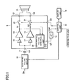
- FIG. 1 is a view showing a configuration of a BTL amplifying system of the first embodiment, and it shows an example in which the invention is employed as an amplifying system incorporated in a stereophonic audio device mounted on a vehicle and used to drive speakers provided to their respective stereo channels.
- the BTL amplifying system of the present embodiment is provided with a BTL amplifier 9 in the form of an IC to serve as an integrated circuit device, an electronic volume circuit 10 for adjusting the amplitude of an input audio signal Sin supplied from a signal source (not shown) and outputting the amplitude-adjusted signal, a coupling capacitor 11, a low-pass filter 12, a control unit 13 equipped with a microprocessor (MPU) , and a display unit 14 composed of a liquid crystal display or the like, and is configured to sound a speaker 15 connected somewhere between the output terminals Q1 and Q2 of the BTL amplifier 9 to serve as a load.
- MPU microprocessor
- the BTL amplifier 9 is provided with a non-inverting amplifying circuit 16 for applying non-inverting amplification to an audio signal supplied at the input terminal Q0 from the electronic volume circuit 10 through the coupling capacitor 11, an inverting amplifying circuit 17 for applying inverting amplification to the audio signal, a power amplifying circuit 18 for applying power amplification to the audio signal having its voltage amplified in the non-inverting amplifying circuit 16, and another power amplifying circuit 19 for applying power amplification to the audio signal having its voltage amplified in the inverting amplifying circuit 17.
- the amplifying circuits 16 and 17 are set to the same voltage gain, and the amplifying circuits 18 and 19 are set to the same power gain.
- these amplifying circuits 16, 17, 18 and 19 can be composed of a generally known direct-coupled amplifying circuit.
- the BTL amplifier 9 of the present embodiment is characterized in that the output contacts of the power amplifying circuits 18 and 19 are connected respectively to the output terminals Q1 and Q2 through switch elements 20 and 21 each composed of an analog switch or the like, and that it is provided with a differential voltage detecting unit 22 for generating a differential voltage signal S12 for detecting an offset, using an output voltage S1 from the power amplifying circuit 18 and an output voltage S2 from the power amplifying circuit 19.
- the BTL amplifier 9 is also provided with an outside input terminal Q3 for supplying a control signal to the switch elements 20 and 21 from the outside, and an outside output terminal Q4 for outputting the differential voltage signal S12 generated in the differential voltage detecting unit 22.
- the outside input terminal Q3 is connected to the control unit 13 and the outside output terminal Q4 is connected to the low-pass filter 12.
- the differential voltage detecting unit 22 is composed of a differential amplifier (not shown) for calculating the difference between the aforementioned output voltages S1 and S2, and a comparator (not shown) for comparing the voltage level of a difference signal (S1 - S2) outputted from the differential amplifier with a certain threshold voltage VTHD.
- the threshold voltage VTHD is determined in advance with consideration given to an allowable offset voltage.
- an offset voltage generated between the output voltages S1 and S2 is within a range such that does not damage or adversely affect the load, such as the speaker 15, the non-occurrence of a practical offset is assumed from the technical view points, and the occurrence of an offset is assumed when the offset voltage would damage the load, such as the speaker 15.
- the offset voltage is judged as being allowable, and a voltage value of the threshold voltage VTHD is determined in advance from experiments or the like with consideration given to the offset voltage judged as being within the allowable range as above.
- the aforementioned comparator outputs the differential voltage signal S12 of a rectangular waveform which shifts to a level "L” upon detection of a difference signal (S1 - S2) at a level higher than the threshold voltage VTHD and to a level "H” upon detection of a difference signal (S1 - S2) at a level equal to or lower than the threshold voltage VTHD.
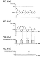
- the output voltages S1 and S2 respectively from the power amplifying circuits 18 and 19 shape inverted-phase waveforms with reference to an output bias voltage Vcc/2, which is half the source voltage Vcc.
- the differential amplifier Given the output voltages S1 and S2 as the targets for detection by the differential amplifier, then, as shown in Fig. 2 (b) , the differential amplifier generates a difference signal (S1 - S2) whose amplitude varies with reference to a certain reference voltage (a voltage 0 in the drawing).
- the aforementioned threshold voltage VTHD is set to a voltage shifted by a certain voltage with respect to the certain reference voltage
- the comparator compares the threshold voltage VTHD with the difference signal (S1 - S2)
- it outputs the differential voltage signal S12 of a rectangular waveform as shown in Fig. 2 (c) .
- the comparator compares the difference signal (S1 - S2) with the threshold voltage VTHD
- it outputs the differential voltage signal S12 as shown in Fig. 2 (c) which stays in the level "H” in a longer period than a period it stays in the level "L” within one duty period T1 during which inversion between the level "L” and the level “H” occurs.
- Fig. 3 (a) when there is an offset, the output voltages S1 and S2 respectively from the power amplifying circuits 18 and 19 shape phase-inverted waveforms shifted by an offset voltage with respect to the output bias voltage Vcc/2. Given the output voltages S1 and S2 as the targets of detection by the differential amplifier, then, as shown in Fig. 3(b), the differential amplifier generates a difference signal (S1 - S2) whose amplitude is shifted with respect to the aforementioned reference voltage (voltage 0).
- the comparator compares the threshold voltage VTHD with the difference signal (S1 - S2) and outputs the differential voltage signal S12 of a rectangular waveform as shown in Fig. 3 (c) . Since the comparator compares the difference signal (S1 - S2) whose amplitude varies as being shifted with respect to the reference voltage (voltage 0) with the threshold voltage VTHD, when an offset occurs between the output voltages S1 and S2 , the comparator outputs the differential voltage signal S12 which stays in the level "H" in a shorter period in comparison with the differential voltage signal S12 generated when there is no offset as shown in Fig. 2 (c) .
- the differential voltage detecting unit 22 detects the difference (S1 - S2) between the output voltages S1 and S2 outputted respectively from the power amplifying circuits 18 and 19, and outputs the differential voltage signal S12 in a duty ratio corresponding to the difference (S1 S2).
- the low-pass filter 12 is composed of a low-pass filter having a band as high as or lower than the audio band, for example, a low frequency band of 20 Hz or lower, as a pass band, and generates a detection signal Vdet of a DC voltage by smoothing the differential voltage signals S12 outputted from the aforementioned outside output terminal Q4 and supplies the detection signal Vdet to the control unit 13.
- the low-pass filter 12 smoothes the differential voltage signal S12 having the longer level "H" period, and thereby outputs the detection signal Vdet of a DC voltage as shown in Fig. 2(d).
- the low-pass filter 12 smoothens the differential voltage signal S12 having the shorter level "H" period, and thereby outputs the detection signal Vdet of a DC voltage as shown in Fig. 3(d).
- the low-pass filter 12 is configured to output the detection signal Vdet indicating the absence/presence of an offset depending on the difference in the voltage levels.
- the control unit 13 is pre-set with a threshold voltage Vok used when making a final judgment as to the absence/presence of an offset.
- the threshold voltage Vok used for the final judgment is also determined in advance with consideration given to a practically allowable offset voltage.
- the control unit 13 compares the voltage level of the detection signal Vdet with the threshold voltage Vok, and judges the absence of an offset in the outputs from the power amplifying circuits 18 and 19 when the voltage level of the detection signal Vdet is higher than the threshold voltage Vok. Conversely, it judges the presence of an offset in the outputs from the power amplifying circuits 18 and 19 when the voltage level of the detection signal Vdet is equal to or lower than the threshold voltage Vok.
- the control unit 13 Upon judging the presence of an offset, the control unit 13 supplies a switching control signal to the switch elements 20 and 21 through the outside input terminal Q3, and brings the switch elements 20 and 21 into a non-conductive state (OFF state) to cut the connection between the power amplifying circuits 18 and 19 and the speaker 15. Upon judging the absence of an offset, the control unit 13 maintains the conductive state (ON state) of the switch elements 20 and 21. Also, the control unit 13 controls the display unit 14 to display a warning or the like when switching the switch elements 20 and 21 to the non-conductive state.
- the control unit 13 performs basic control, for example, it adjusts a volume of the speaker 15 by receiving command information supplied from an operation panel (not shown) or the like manipulated by the user and controlling an operation of the electronic volume circuit 10 at a command from the user. Also, it controls the turn-ON and turn-OFF of the power of the BTL amplifying system in response to the set position of the ignition key of the vehicle, the ON/OFF position of the main power switch, etc. each manipulated by the user.
- Step S100 a command to turn ON the power is made as the user switches ON the main power switch provided to the audio device or the user manipulates and sets the ignition key of the vehicle to the starting position.
- Step S102 the control unit 13 turns ON the power of the BTL amplifying system.
- an input audio signal Sin played back from a signal source such as a radio receiver, an MD (Mini Disc) player, a CD (Compact Disc) player, and a DVD (Digital Versatile Disc) player provided to the audio device is supplied to the BTL amplifier 9 through the electronic volume circuit 10 and the coupling capacitor 11.
- the BTL amplifier 9 thus amplifies the input audio signal Sin and sounds the speaker 15.
- the BTL amplifying system starts an amplifying operation as soon as the power is turned ON, and continues to perform Steps S104 through S112 described below along with the amplifying operation.
- Step S104 when the BTL amplifier 9 starts the amplifying operation, the differential voltage detecting unit 22 calculates the difference (S1- S2) between the output voltages S1 and S2 respectively from the power amplifying circuits 18 and 19, and generates the differential voltage signal S12 by comparing the difference (S1 S2) with the threshold voltage VTHD.
- the low-pass filter 12 then generates the detection signal Vdet by smoothing the differential voltage signal S12, and outputs the detection signal Vdet to the control unit 13.
- Step S106 the control unit 13 compares the pre-set threshold voltage Vok with the detection signal Vdet, and judges whether the voltage level of the detection signal Vdet is higher than the threshold voltage Vok.
- the flow proceeds to Step S108, where the control unit 13 judges the absence of an offset between the output voltages S1 and S2, and in Step S110, it judges whether the user has inputted a command to turn OFF the power.
- Step S110 it judges whether the user has inputted a command to turn OFF the power.
- the flow returns to Step S104 and the processing is repeated.
- the control unit 13 stops a supply of power to the BTL amplifying system in Step S112 and ends the series of processing.
- Step S106 when it is judged that the voltage level of the detection signal Vdet is equal to or lower than the threshold voltage Vok (that is, Vdet ⁇ Vok) in Step S106, the flow proceeds to Step S114, where the control unit 13 judges the occurrence of an offset between the output voltages S1 and S2.
- Step S116 the control unit 13 switches both the switch elements 20 and 21 to the OFF state and thereby cuts the connection between the power amplifying circuits 18 and 19 and the speaker 15. The speaker 15 is thus stopped sounding. Further, in subsequent Step S118, the control unit 13 controls the display unit 14 to display a warning of the occurrence of an abnormality. Then, the control unit 13 forcedly stops a supply of power to the BTL amplifying system in Step S112, and ends the series of processing.
- the BTL amplifying system of the present embodiment continues to detect the absence/presence of an offset since the instant the power is turned ON, and forcedly turns OFF the power when the offset exceeds an allowable range.
- the detection of the absence/presence of an offset is continued while the input audio signal Sin from the sound source is amplified to sound the speaker 15. Consequently, should a DC offset current flow into the speaker 15 while the speaker 15 is sounded continuously as leakage occurs due to deterioration with time of the coupling capacitor 11 or the characteristic of the BTL amplifier 9 varies due to the influence of use environments, an offset being occurred can be detected as soon as possible and the power is turned OFF. This makes it possible to forestall a problem, for example, the speaker 15 is damaged due to heat generated by the offset current.
- Fig. 5 is a view showing a configuration of the BTL amplifying system, and like components with respect to the BTL amplifying system of Fig. 1 are labeled with like reference numerals.
- the BTL amplifying system of the present embodiment is configured in such a manner that the switch elements 20 and 21 shown in Fig. 1 are omitted, and the output contacts of the power amplifying circuits 18 and 19 are directly connected to the output terminals Q1 and Q2, respectively. Instead, activating/deactivating circuits 18a and 19a are provided respectively to the power amplifying circuits 18 and 19 to allow them to stop their own power amplifying operations.
- an unillustrated constant current source circuit composed of a current mirror circuit or the like is provided to each of the power amplifying circuits 18 and 19, and the output voltages S1 and S2 for driving the speaker 15 are generated by applying power amplification to currents outputted from the constant current source circuits according to the audio signals outputted from the non-inverting amplifying circuit 16 and the inverting amplifying circuit 17, respectively.
- the activating/deactivating circuits 18a and 19a stop the generation of the output voltages S1 and S2 by interrupting the currents outputted from the aforementioned constant current source circuits.
- the BTL amplifying system configured as above continues to perform the same offset detection processing as that in the first embodiment described with reference to Figs. 2(a) through 2(d) and Figs. 3 and 4.
- the differential voltage detecting unit 22 calculates the difference (S1- S2) between the output voltages S1 and S2 respectively from the power amplifying circuits 18 and 19, and generates the differential voltage signal S12 by comparing the difference (S1 - S2) with the threshold voltage VTHD.
- the low-pass filter 12 then generates the detection signal Vdet by smoothing the differential voltage signal S12 and outputs the detection signal Vdet to the control unit 13.
- control unit 13 judges the occurrence of an offset upon detection of the detection signal Vdet having a level equal to or lower than the threshold voltage Vok, and controls the activating/deactivating circuits 18a and 19a in such a manner that the power amplifying circuits 18 and 19 stop their own power amplifying operations.
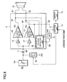
- Fig. 6 is a view showing a configuration of the BTL amplifying system of the present embodiment, and like components with respect to the BTL amplifying system of Fig. 5 are labeled with like reference numerals.
- the BTL amplifying system of the present embodiment is provided with a mechanical attenuator 10a instead of the electronic volume circuit 10 to allow the user to variably adjust a quantity of attenuation of the input audio signal Sin by hand, and a switch element 23 is connected somewhere between the output contact of the mechanical attenuator 10a and the ground terminal GND provided to the BTL amplifying system.
- the control unit 13 controls the ON/OFF operation of the switch element 23.
- the BTL amplifying system configured as above continues to perform the same offset detection processing as that in the first embodiment explained with reference to Fig. 2 (a) through 2 (d) and Figs. 3 and 4.
- the control unit 13 sets the switch element 23 to the OFF state.
- the input audio signal is thus inputted to the BTL amplifier 9 and a normal amplifying operation is performed.
- the differential voltage detecting unit 22 calculates the difference (S1 S2) between the output voltages S1 and S2 respectively from the power amplifying circuits 18 and 19, and generates the differential voltage signal S12 by comparing the difference (S1-S2) with the threshold voltage VTHD.
- the low-pass filter 12 then generates the detection signal Vdet by smoothing the differential voltage signal S12, and outputs the detection signal Vdet to the control unit 13.
- the control unit 13 judges the occurrence of an offset, and controls the activating/deactivating circuits 18a and 19a in such a manner that the power amplifying circuits 18 and 19 stop their own power amplifying operations.
- control unit 13 upon judging the occurrence of an offset, not only controls the power amplifying circuits 18 and 19 to stop their own power amplifying operations, but also controls the switch element 23 to switch from the OFF state to the ON state, so that the audio signal from the attenuator 10a is muted and thereby prevented from being supplied to the coupling capacitor 11.
- an input of the audio signal itself is stopped upon the occurrence of an offset, and therefore, not only can the speaker 15 be protected in a reliable manner, but also the BTL amplifier 9 can be protected.
- the electronic amplifying circuits 18 and 19 may be configured in such a manner that they are not provided with the aforementioned activating/deactivating circuits 18a and 19a, and merely control the switch element 23 to be ON when the occurrence of an offset is detected. In short, by inhibiting a supply of the input audio signal to the BTL amplifier 9, it is possible to prevent an offset voltage from being applied to the speaker 15 in advance.
- the BTL amplifying system of Fig. 6 is configured in such a manner that the switch element 23 is connected to the outside at somewhere between the input side contact of the coupling capacitor 11 and the ground terminal GND.
- the present embodiment may be modified as shown in Fig. 7, in which the switch element 23 composed of an analog switch or the like is pre-formed in the interior of the BTL amplifier 9, and upon judging the occurrence of an offset based on the detection signal Vdet, the control unit 13 controls the switch element 23 to be ON through a control signal input terminal Q5, so that an input of the audio signal to the non-inverting amplifying circuit 16 and to the inverting amplifying circuit 17 is inhibited.
- the mechanical attenuator 10a and the switch element 23 of the present embodiment may be provided to the BTL amplifying system of the first embodiment shown in Fig. 1.
- the detection signal Vdet of a DC voltage is obtained by smoothing the differential voltage signal S12 of a rectangular waveform outputted from the differential voltage detecting unit 22 in the low-pass filter 12. It shouldbe appreciated, however, that the invention is not limited to cases where the detection signal Vdet is obtained in the low-pass filter 12.
- the low-pass filter 12 may be replaced with a re-settable timer circuit or counter circuit which is connected somewhere between the terminal Q4 and the control unit 13, so that periods during which the differential voltage signal S12 stays in the level “H” and in the level “L” in one duty period are measured by the timer circuit or the counter circuit, and the result of measurement is supplied to the control unit 13 instead of the detection signal Vdet. Then, the control unit 13 detects a duty ratio of the level "H” period and the level "L” period from the result of measurement, compares the duty ratio with pre-set threshold data used to judge an offset, and makes a final judgment as to the occurrence of an offset.
- the aforementioned timer circuit or counter circuit may be pre-formed in the interior of the BTL amplifier 9 together with the differential voltage detecting unit 22, so that data of the result of measurement outputted from the timer circuit or the counter circuit is outputted from the terminal Q4.
- the differential voltage detecting unit 22 is provided so that the difference (S1-S2) between the output voltages S1 and S2 outputted respectively from the power amplifying circuits 18 and 19 is calculated, and the differential voltage signal S12 of a rectangular waveform is generated by comparing the difference (S1 - S2) with the threshold voltage VTHD.
- a signal of the same rectangular waveform as that of the aforementioned differential voltage signal S12 may be generated by comparing a change in either of the output voltages S1 and S2 with a certain threshold voltage VTHD', so that this signal is smoothed in the low-pass filter 12 or measured by the timer circuit or the counter circuit.
- the threshold voltage VTHD' is set to the sum of a voltage Vcc/2, which is half the source voltage Vcc, and a voltage VTHD/2, which is half the aforementioned threshold voltage VTHD, that is, a voltage expressed as (Vcc + VTHD) /2. Then, a signal of a rectangular waveform is generated, which shifts to the level "L” when the output voltage S1 has a level higher than the threshold voltage VTHD', and to the level "H” when the output voltage S1 has a level equal to or lower than the threshold voltage VTHD'. The signal thus generated is outputted instead of the aforementioned differential voltage signal S12.
- the threshold voltage VTHD' is set to the difference between a voltage Vcc/2, which is half the source voltage Vcc, and a voltage VTHD/2, which is half the aforementioned threshold voltage VTHD, that is, a voltage expressed as (Vcc - VTHD)/2. Then, a signal of a rectangular waveform is generated, which shifts to the level “L” when the output voltage S2 has a level equal to or lower than the threshold voltage VTHD' , and to the level "H” when the output voltage S2 has a level higher than the threshold voltage VTHD' . The signal thus generated is outputted instead of the aforementioned differential voltage signal S12.
- processing to detect and judge the occurrence of an offset may be repeated at predetermined regular intervals (for example, every second, every 10 seconds, every minute, or every hour), and the driving of the speaker 15 is stopped at the instant the occurrence of an offset is judged.
- the predetermined regular interval may differ in a certain time period immediately after the turn-ON of the power of the BTL amplifying system and in the period after this certain period has passed. The important point is that a countermeasure against an offset that best suits the situation can be provided by setting the timing at which the so-called constant detection is performed while the speaker 15 is driven according to practical use.
- a command maybe issued from the outside while the speaker 15 is driven to detect the occurrence of an offset.
- the control unit 13 may control the differential voltage detecting unit 22 to start to detect the output voltages S1 and S2, so that the control unit 13 judges the occurrence of an offset based on the detection result.
- the user or an inspection technical expert can check the operation status of the BTL amplifying system, which offers an advantage that accidents of various kinds can be prevented in advance.
- the occurrence of an offset is detected and judged while the power amplifying circuits of the BTL configuration are driving the load, and the driving operation is stopped upon detection and judgment of the occurrence of an offset.
Landscapes
- Engineering & Computer Science (AREA)
- Power Engineering (AREA)
- Amplifiers (AREA)
- Circuit For Audible Band Transducer (AREA)
Applications Claiming Priority (2)
| Application Number | Priority Date | Filing Date | Title |
|---|---|---|---|
| JP2002054034 | 2002-02-28 | ||
| JP2002054034A JP2003258575A (ja) | 2002-02-28 | 2002-02-28 | Btl増幅装置 |
Publications (2)
| Publication Number | Publication Date |
|---|---|
| EP1341302A2 true EP1341302A2 (de) | 2003-09-03 |
| EP1341302A3 EP1341302A3 (de) | 2005-01-26 |
Family
ID=27678561
Family Applications (1)
| Application Number | Title | Priority Date | Filing Date |
|---|---|---|---|
| EP03004276A Withdrawn EP1341302A3 (de) | 2002-02-28 | 2003-02-26 | Symmetrisches Verstärkersystem ohne Transformator |
Country Status (3)
| Country | Link |
|---|---|
| US (1) | US6806766B2 (de) |
| EP (1) | EP1341302A3 (de) |
| JP (1) | JP2003258575A (de) |
Cited By (1)
| Publication number | Priority date | Publication date | Assignee | Title |
|---|---|---|---|---|
| DE10307917B4 (de) * | 2003-02-25 | 2005-05-25 | Sukalo, Drazenko, Dipl.-Ing. | Subwoofer-System mit dynamischem Pushpull-Antrieb |
Families Citing this family (15)
| Publication number | Priority date | Publication date | Assignee | Title |
|---|---|---|---|---|
| JP2006054693A (ja) * | 2004-08-12 | 2006-02-23 | Matsushita Electric Ind Co Ltd | 携帯電話装置 |
| US7394312B2 (en) * | 2004-11-15 | 2008-07-01 | Pioneer Corporation | Re-configurable amplifier protection apparatus and method |
| JP2006278107A (ja) * | 2005-03-29 | 2006-10-12 | Sharp Corp | 面照明装置及びそれを備えた液晶表示装置 |
| JP2007088921A (ja) * | 2005-09-22 | 2007-04-05 | Matsushita Electric Ind Co Ltd | スピーカ保護回路 |
| US7332969B2 (en) | 2005-10-31 | 2008-02-19 | Matsushita Electric Industrial Co., Ltd. | Output offset protection for power amplifier |
| US7427893B2 (en) * | 2006-06-15 | 2008-09-23 | Kwang-Hwa Liu | Circuit and method for controlling the power mode a class-D amplifier |
| US7671675B2 (en) | 2007-08-20 | 2010-03-02 | Rohm Co., Ltd. | Output limiting circuit, class D power amplifier and audio equipment |
| KR101120629B1 (ko) * | 2008-04-18 | 2012-03-19 | 페어차일드 세미컨덕터 코포레이션 | 증폭기 전류 구동 반전 |
| JP5206763B2 (ja) * | 2010-10-21 | 2013-06-12 | オンキヨー株式会社 | 増幅装置 |
| CN106412761B (zh) | 2011-12-30 | 2020-02-14 | 意法半导体研发(深圳)有限公司 | 用于汽车音频功率放大器的嵌入式扬声器保护 |
| WO2016051583A1 (ja) * | 2014-10-03 | 2016-04-07 | パイオニア株式会社 | オフセット電圧監視装置及びオフセット電圧監視方法 |
| JP6767219B2 (ja) * | 2016-09-21 | 2020-10-14 | 株式会社東芝 | オフセット検出回路 |
| JP2018205223A (ja) * | 2017-06-08 | 2018-12-27 | 三菱電機株式会社 | ゲイン制御増幅装置 |
| JP2019054519A (ja) * | 2018-10-17 | 2019-04-04 | パイオニア株式会社 | オフセット電圧監視装置及びオフセット電圧監視方法 |
| CN118280428B (zh) * | 2024-06-03 | 2024-09-20 | 芯梦达半导体科技(济南)有限公司 | 内存检测方法及其检测系统 |
Family Cites Families (3)
| Publication number | Priority date | Publication date | Assignee | Title |
|---|---|---|---|---|
| JP3495620B2 (ja) * | 1998-12-04 | 2004-02-09 | パイオニア株式会社 | Btl増幅装置 |
| JP3474825B2 (ja) * | 2000-03-13 | 2003-12-08 | 富士通カンタムデバイス株式会社 | 高周波電力増幅器および通信装置 |
| KR20030014253A (ko) * | 2001-03-29 | 2003-02-15 | 코닌클리케 필립스 일렉트로닉스 엔.브이. | Btl증폭기 및 이를 위한 옵셋 검출 및 보정 시스템 |
-
2002
- 2002-02-28 JP JP2002054034A patent/JP2003258575A/ja active Pending
-
2003
- 2003-02-20 US US10/368,487 patent/US6806766B2/en not_active Expired - Fee Related
- 2003-02-26 EP EP03004276A patent/EP1341302A3/de not_active Withdrawn
Cited By (1)
| Publication number | Priority date | Publication date | Assignee | Title |
|---|---|---|---|---|
| DE10307917B4 (de) * | 2003-02-25 | 2005-05-25 | Sukalo, Drazenko, Dipl.-Ing. | Subwoofer-System mit dynamischem Pushpull-Antrieb |
Also Published As
| Publication number | Publication date |
|---|---|
| US6806766B2 (en) | 2004-10-19 |
| US20030160653A1 (en) | 2003-08-28 |
| JP2003258575A (ja) | 2003-09-12 |
| EP1341302A3 (de) | 2005-01-26 |
Similar Documents
| Publication | Publication Date | Title |
|---|---|---|
| US6806766B2 (en) | BTL amplifying system | |
| EP1244208B1 (de) | Leistungsverstärker | |
| US7092533B1 (en) | BTL amplifier apparatus | |
| CN109752608B (zh) | 负载检测器 | |
| US8180072B2 (en) | Electronic volume device | |
| JPH05315856A (ja) | 電力増幅装置 | |
| US10476446B2 (en) | Total harmonic distortion (THD) controlled clip detector and automatic gain limiter (AGL) | |
| US7332969B2 (en) | Output offset protection for power amplifier | |
| US5148115A (en) | Load connection state detector circuit | |
| US10622957B2 (en) | Integrated circuit, circuit assembly and a method for its operation | |
| JP2003304123A (ja) | オーディオアンプ及びその異常検出方法 | |
| US7679508B2 (en) | Sensing device for detecting approaching object | |
| CN103424625B (zh) | 测试信号供应设备和半导体集成电路 | |
| JP2007074119A (ja) | ショート検出回路 | |
| JP6528491B2 (ja) | 電力増幅器 | |
| KR910009479Y1 (ko) | 스피커의 저역 보상회로 | |
| US7697908B2 (en) | Duty-to-voltage amplifier, FM receiver and method for amplifying a peak of a multiplexed signal | |
| JP2009171068A (ja) | スピーカ接続状態検出方法 | |
| KR20000013911U (ko) | 스피커 임피던스 정합 장치 | |
| JP3355065B2 (ja) | スピーカラインの検査装置 | |
| JP2000098009A (ja) | 磁気検出センサ | |
| US20070165893A1 (en) | Howling margin measuring device | |
| JP2009260834A (ja) | 過電流保護回路及びd級アンプ | |
| KR200319847Y1 (ko) | 스피커 임피던스 보호장치 | |
| JP2004221885A (ja) | 電力増幅装置および電力増幅システム |
Legal Events
| Date | Code | Title | Description |
|---|---|---|---|
| PUAI | Public reference made under article 153(3) epc to a published international application that has entered the european phase |
Free format text: ORIGINAL CODE: 0009012 |
|
| AK | Designated contracting states |
Kind code of ref document: A2 Designated state(s): AT BE BG CH CY CZ DE DK EE ES FI FR GB GR HU IE IT LI LU MC NL PT SE SI SK TR |
|
| AX | Request for extension of the european patent |
Extension state: AL LT LV MK RO |
|
| PUAL | Search report despatched |
Free format text: ORIGINAL CODE: 0009013 |
|
| AK | Designated contracting states |
Kind code of ref document: A3 Designated state(s): AT BE BG CH CY CZ DE DK EE ES FI FR GB GR HU IE IT LI LU MC NL PT SE SI SK TR |
|
| AX | Request for extension of the european patent |
Extension state: AL LT LV MK RO |
|
| 17P | Request for examination filed |
Effective date: 20050509 |
|
| AKX | Designation fees paid |
Designated state(s): DE FR GB IT NL |
|
| GRAP | Despatch of communication of intention to grant a patent |
Free format text: ORIGINAL CODE: EPIDOSNIGR1 |
|
| STAA | Information on the status of an ep patent application or granted ep patent |
Free format text: STATUS: THE APPLICATION HAS BEEN WITHDRAWN |
|
| 18W | Application withdrawn |
Effective date: 20071001 |