EP1298734A2 - Module for optical communications for converting light to differential signals - Google Patents
Module for optical communications for converting light to differential signals Download PDFInfo
- Publication number
- EP1298734A2 EP1298734A2 EP02020556A EP02020556A EP1298734A2 EP 1298734 A2 EP1298734 A2 EP 1298734A2 EP 02020556 A EP02020556 A EP 02020556A EP 02020556 A EP02020556 A EP 02020556A EP 1298734 A2 EP1298734 A2 EP 1298734A2
- Authority
- EP
- European Patent Office
- Prior art keywords
- pattern
- major surface
- wiring
- intersecting
- connection terminal
- Prior art date
- Legal status (The legal status is an assumption and is not a legal conclusion. Google has not performed a legal analysis and makes no representation as to the accuracy of the status listed.)
- Withdrawn
Links
Images


Classifications
-
- H—ELECTRICITY
- H10—SEMICONDUCTOR DEVICES; ELECTRIC SOLID-STATE DEVICES NOT OTHERWISE PROVIDED FOR
- H10F—INORGANIC SEMICONDUCTOR DEVICES SENSITIVE TO INFRARED RADIATION, LIGHT, ELECTROMAGNETIC RADIATION OF SHORTER WAVELENGTH OR CORPUSCULAR RADIATION
- H10F77/00—Constructional details of devices covered by this subclass
- H10F77/93—Interconnections
- H10F77/933—Interconnections for devices having potential barriers
-
- H—ELECTRICITY
- H10—SEMICONDUCTOR DEVICES; ELECTRIC SOLID-STATE DEVICES NOT OTHERWISE PROVIDED FOR
- H10F—INORGANIC SEMICONDUCTOR DEVICES SENSITIVE TO INFRARED RADIATION, LIGHT, ELECTROMAGNETIC RADIATION OF SHORTER WAVELENGTH OR CORPUSCULAR RADIATION
- H10F77/00—Constructional details of devices covered by this subclass
- H10F77/50—Encapsulations or containers
-
- H—ELECTRICITY
- H01—ELECTRIC ELEMENTS
- H01L—SEMICONDUCTOR DEVICES NOT COVERED BY CLASS H10
- H01L2224/00—Indexing scheme for arrangements for connecting or disconnecting semiconductor or solid-state bodies and methods related thereto as covered by H01L24/00
- H01L2224/01—Means for bonding being attached to, or being formed on, the surface to be connected, e.g. chip-to-package, die-attach, "first-level" interconnects; Manufacturing methods related thereto
- H01L2224/42—Wire connectors; Manufacturing methods related thereto
- H01L2224/47—Structure, shape, material or disposition of the wire connectors after the connecting process
- H01L2224/48—Structure, shape, material or disposition of the wire connectors after the connecting process of an individual wire connector
- H01L2224/4805—Shape
- H01L2224/4809—Loop shape
- H01L2224/48091—Arched
Definitions
- the present invention relates to a module for optical communications, for example, which coverts a light signal to signals of a differential form and outputs the signals, or which emits the light signal in response to the inputted differential signals.
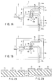
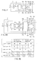
- FIG. 10A schematically shows a first example of a conventional module for the optical communications.
- a module for optical communications 101 includes a package 102 in which a light receiving element and wiring substrate described later are contained.
- a light receiving element 104 which receives a light incident from an optical fiber 103 and photoelectrically converts the light
- a wiring substrate 105 On the wiring substrate 105, there are disposed: semiconductor devices (hereinafter referred to as IC) such as a preamplifier 106 which amplifies a signal from the light receiving element 104; and wiring patterns 107a, 107b.
- IC semiconductor devices
- a differential output form has frequently been used which has a reverse and non-reverse outputs in order to enhance an SN ratio with respect to an external noise.
- a connection pad 108a formed on an upper side outputs the non-reverse output
- a connection pad 108b on a lower side outputs the reverse output.
- the wiring patterns 107a, 107b substantially have symmetric shapes in a perpendicular direction, and these wiring patterns 107a, 107b are disposed opposite to each other.
- the connection pads 108a, 108b and wiring patterns 107a, 107b are connected to each other via bonding wires 109.
- the wiring patterns 107a, 107b are connected to lead pins 110a, 110b in ends of the wiring substrate 105.
- the above-described module for optical communications 101 is disposed, for example, on a substrate, and the substrate is assembled in various apparatuses for use.
- FIG. 11 shows a second conventional example of the module for optical communications.
- a module for optical communications 121 includes the light receiving element 104 and wiring substrate 105 in the package 102.
- An IC 122 is disposed on the wiring substrate 105.
- the IC 122 includes a connection pin 123a which outputs the reverse output and a connection pin 123b which outputs the non-reverse output.
- the connection pins 123a, 123b are connected to wiring patterns 124a, 124b.
- the wiring patterns 124a, 124b are respectively connected to the lead pins 110a, 110b, for example, via bonding wires.
- the lead pin 110a is connected to the connection pad 108a to output the non-reverse output
- the lead pin 110b is connected to the connection pad 108b to output the reverse output.
- the arrangement of these lead pins is not optionally determined.
- a side on which the connection pads 108a, 108b of the IC 106 are formed does not meet with a side on which the lead pins 110a, 110b are formed. That is, the lead pin 110a forms the reverse output, and the lead pin 110b forms the non-reverse output.
- connection pad 108a forms the reverse output
- the lower connection pad 108b forms the non-reverse output. This increases costs.
- the IC with a connection pad arrangement that meets the demand of a user may not be manufactured.
- connection relations between the connection pads 108a, 108b and lead pins 110a, 110b need to be reversed.
- a method comprising: allowing the bonding wires 109 for connecting the connection pads 108a, 108b to the wiring patterns 107a, 107b to intersect with each other. That is, the connection pad 108a is connected to the wiring pattern 107b, and the connection pad 108b is connected to the wiring pattern 107a.
- connection pins 123a, 123b of the IC 122 may not be on the same side as the lead pins 110a, 110b in some cases.
- a module for optical communications comprising: a light receiving element receiving the light signal and converting the light signal to an electric signal; an insulating substrate including a first major surface and a second major surface opposite to the first major surface; an output section provided on the first major surface and extracting the electric signal as a reverse signal and non-reverse signal; first and second connection terminals connected to the output section, the reverse signal being outputted via the first connection terminal, the non-reverse signal being outputted via the second connection terminal; and first and second wiring patterns provided on the first major surface, one of the first and second wiring patterns being electrically connected to the first connection terminal, the other one of the first and second wiring patterns being electrically connected to the second connection terminal, the first wiring pattern including a first end, the second wiring pattern including a second end, and the first and second ends being provided in order in a direction intersecting with a line connecting the first and second connection terminals.
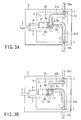
- FIG. 1A schematically shows a module for optical communications according to a first embodiment of the present invention.
- a module for optical communications 1 includes a package (envelope) 2 in which a light receiving element and wiring substrate described later are contained.
- the package 2 there are disposed: an optical fiber 3; a light receiving element 4 which receives a light signal incident from the optical fiber 3; and a wiring substrate 5 disposed adjacent to the light receiving element 4.
- the wiring substrate 5 is formed, for example, of silicon and ceramic such as alumina (Al 2 O 3 ), aluminum nitride (AlN) and silicon nitride (Si 3 N 4 ).
- an IC 6 is disposed opposite to the light receiving element 4.
- the IC 6 includes a preamplifier which is connected to the light receiving element 4 via bonding wires 7 and which amplifies a signal from the light receiving element 4 and outputs differential signals.
- the IC 6 includes a connection pad 8a which forms a non-reverse output, and a connection pad 8b which forms a reverse output.
- the connection pads (connection terminals) 8a, 8b are arranged along a side disposed opposite to a side on which, for example, the light receiving element 4 is disposed.
- wiring patterns 9a, 9b are disposed on the wiring substrate 5.
- the wiring patterns 9a, 9b are connected to the connection pads 8a, 8b via bonding wires 7a, 7b.
- Each of the wiring patterns 9a, 9b can be formed as a so-called coplanar line in which a signal electrode line is formed in a middle and ground electrodes are formed at a predetermined interval in opposite ends.
- a signal electrode line is formed in a middle and ground electrodes are formed at a predetermined interval in opposite ends.
- the respective bonding wires 7a, 7b are connected to the wiring patterns 9a, 9b. This means that the wires are connected to the signal electrode lines, unless otherwise specified.
- the coplanar line will be described later in detail.
- the wiring patterns 9a, 9b include, for example, first ends 10a, 10b, and second ends 11a, 11b and have substantially L shapes.
- the wiring patterns 9a, 9b are disposed vertically adjacent to each other.
- the upper wiring pattern 9a is disposed such that a character L is rotated in a clockwise direction by 90 degrees.
- the lower wiring pattern 9b is disposed such that the wiring pattern 9a is further rotated in a clockwise direction by 90 degrees.
- the first end 10a of the wiring pattern 9a is disposed not to contact the side on which the connection pads 8a, 8b are disposed.
- the first end 10b of the wiring pattern 9b is disposed opposite to the side on which the connection pads 8a, 8b of the IC 6 are disposed via the wiring pattern 9a in a non-contact state.
- the second ends 11a, 11b of the wiring patterns 9a, 9b are positioned in the ends of the wiring substrate 5.
- the wiring patterns 9a, 9b do not contact each other.
- the second end 11a of the wiring pattern 9a is connected to a lead pin 12a via the bonding wire 7, and the second end 11b of the wiring pattern 9b is connected to a lead pin 12b via the bonding wire 7.
- a resist 13 consisting of an insulating film such as resin is formed on the wiring pattern 9a disposed between the wiring pattern 9b and IC 6.
- the bonding wire 7a is disposed over the resist 13.
- a light signal incident from the optical fiber 3 is converted to an electric signal by the light receiving element 4.
- the electric signal converted by the light receiving element 4 is amplified by the IC 6, and outputted as non-reverse and reverse output signals to the outside of the package 2 from the lead pins 12a, 12b via the wiring patterns 9a, 9b.
- FIG. 1B schematically shows a constitution in which positions of the reverse and non-reverse outputs of the module for optical communications 1 constituted as described above are reversed, the lead pin 12a forms the reverse output, and the lead pin 12b forms the non-reverse output.
- the bonding wire 7a connected to the connection pad 8a of the non-reverse output of the IC 6 is connected to the wiring pattern 9b over the resist 13.
- the bonding wire 7b connected to the connection pad 8b of the reverse output of the IC 6 is connected to the wiring pattern 9a. Therefore, the lead pin 12a corresponds to the reverse output, and the lead pin 12b corresponds to the non-reverse output.
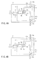
- FIG. 2A is a sectional view schematically showing the structure of the coplanar line.
- a signal electrode line 22 is formed substantially in a middle on a substrate 21.
- Ground electrode lines 23 are formed, for example, at a gap of about 0.1 mm on opposite sides of the signal electrode line 22.
- the substrate 21 in FIG. 2 corresponds to the wiring substrate 5 in the first embodiment shown in FIGS. 1A and 1B. FIG. 2B will be described later.
- two substantially L-shaped wiring patterns 9a, 9b are disposed on the wiring substrate 5, one end of the wiring pattern 9a is disposed adjacent to the IC 6 with a predetermined interval, and one end of the wiring pattern 9b is further disposed adjacent to one end of the wiring pattern 9a.
- the wiring patterns 9a, 9b are disposed vertically adjacent to each other with angles different from each other by 90 degrees. Therefore, a connection relation between the bonding wires 7a, 7b connecting the wiring patterns 9a, 9b to the connection pads 8a, 8b is changed, and then the disagreement of the positional relations can be adjusted.
- the bonding wires 109 do not have to intersect with each other. Therefore, it is possible to avoid short-circuiting the bonding wires 7a, 7b, and the deterioration of the frequency characteristics by the mutual inductance and parasitic capacity between the bonding wires 7a, 7b.
- the lead pins 12a, 12b can be set to desired outputs. Therefore, it is unnecessary to newly prepare the wiring substrate which satisfies the desired wiring pattern, or to separately prepare an IC in which the connection pads 8a, 8b correspond to the desired outputs. Therefore, a manufacturing cost of the module for optical communications 1 can be reduced.
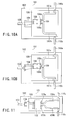
- FIG. 3A schematically shows the module for optical communications according to a second embodiment of the present invention.
- FIG. 3B schematically shows that the relation between the reverse and non-reverse outputs of the lead pins 12a, 12b of the module for optical communications shown in FIG. 3A.
- the coplanar lines in which the ground electrode is not disposed in the back surface of the wiring substrate 5 are used.
- grounded coplanar lines 31a, 31b in which the ground electrode is formed on the back surface of the wiring substrate 5 are used.
- Reference numeral 32 denotes through holes. The other parts are similar to those of the first embodiment.
- FIG. 2B schematically shows the structure of the grounded coplanar line.
- the grounded coplanar line includes a structure in which a ground electrode 24 is disposed over the back surface of the substrate 21.
- FIG. 4A schematically shows the module for optical communications according to a third embodiment of the present invention.
- FIG. 4B schematically shows that the relation between the reverse and non-reverse outputs of the lead pins 12a, 12b of the module for optical communications shown in FIG. 4A is changed.
- the wiring substrate 5 silicon, ceramic, and the like are used as the wiring substrate 5, and the coplanar line or grounded coplanar line is used as the wiring patterns 9a, 9b.
- the wiring patterns 9a, 9b wiring patterns 41a, 41b including a normal structure (micro strip structure) are used, and a material having a high permittivity is used as the wiring substrate 5.
- the material having the high permittivity include sapphire, arsenic gallium, barium titanate-based dielectric material, perovskite dielectric material, and the like.
- FIG. 5A schematically shows the module for optical communications according to a fourth embodiment of the present invention.
- a module for optical communications 51, the optical fiber 3, light receiving element 4, and wiring substrate 5 disposed adjacent to the light receiving element 4 are disposed in the package 2.
- the IC 6 such as the preamplifier is disposed opposite to the light receiving element 4.
- the connection pad 8a of the IC 6 corresponds, for example, to the non-reverse output, and the pad 8b corresponds to the reverse output.
- wiring patterns 35a, 35b are connected to connection pins 8a, 8b.
- the wiring patterns 35a, 35b includes, for example, major portions which have linear shapes. Moreover, the wiring patterns 35a, 35b are vertically disposed substantially in parallel to each other with a predetermined interval. Moreover, as described above, one part of each pattern is bent so that one end of the pattern is connected to each of the connection pins 8a, 8b of the IC 6. This bent shape may be any shape as long as one end of the wiring patterns 35a, 35b are formed so as to be connected to the connection pins 8a, 8b of the IC 6.
- Linear portions of the wiring patterns 35a, 35b have void portions 36a, 36b of the patterns substantially in the middle thereof. These portions are formed so as to be non-conductive, and thereby each pattern is separated into two parts. That is, the wiring pattern 35a includes first and second wiring patterns 35c and 35d. One end of the first wiring pattern 35c is connected to the connection pin 8a. One end of the second wiring pattern 35d is disposed opposite to the other end of the first wiring pattern 35c via the void portion 36a. Similarly, the wiring pattern 35b includes third and fourth wiring patterns 35e and 35f. One end of the third wiring pattern 35e is connected to the connection pin 8b. One end of the fourth wiring pattern 35f is disposed opposite to the other end of the third wiring pattern 35e via the void portion 36b.
- second intersecting patterns 37a, 37b are disposed between the wiring patterns 35a, 35b.
- the first wiring pattern 37a is disposed on the surface of the wiring substrate 5.
- one end of the first intersecting pattern 37a has an interval from the other end of the first wiring pattern 35c, and the other end thereof has an interval from one end of the fourth wiring pattern 35f.
- FIGS. 5B and 5C are diagrams showing one example of a section taken along the second intersecting pattern 37b of FIG. 5A. Additionally, in these drawings, the first intersecting pattern 37a is omitted. As shown in FIG. 5A, one end of the second intersecting pattern 37b has an interval from one end of the second wiring pattern 35d in the surface of the wiring substrate 5. Moreover, the other end also has an interval from the other end of the third wiring pattern 35e. Moreover, as shown in FIG.
- the connecting portion of the second intersecting pattern 37b is disposed on the back surface of the wiring substrate 5. These opposite ends and connecting portion of the second intersecting pattern are connected to one another via through holes 38 formed in the wiring substrate 5. Furthermore, as shown in FIG. 5C, the wiring substrate 5 may have a multilayered structure. In this case, the connecting portion can be disposed between the layers.
- the second and fourth wiring patterns 35d, 35f are connected to the lead pins 12a, 12b via the bonding wires 7.
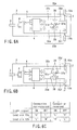
- FIGS. 6A and 6B schematically show the connected state of the wiring patterns 35a, 35b to the first and second intersecting patterns 37a, 37b in the module for optical communications 51 shown in FIG. 5A.
- a method of connecting the wiring patterns 35a, 35b to the first and second intersecting patterns 37a, 37b will be described hereinafter with reference to FIGS. 6A and 6B.
- connection patterns 39 are disposed to electrically connect the void portion 36a of the wiring pattern 35a.
- the first wiring pattern 35c is connected to the second wiring pattern 35d, and the lead pin 12a outputs the non-reverse output.
- the connection patterns 39 are disposed to electrically connect the void portion 36b of the wiring pattern 35b.
- the third wiring pattern 35e is connected to the fourth wiring pattern 35f, and the lead pin 12b outputs the reverse output.
- connection patterns 39 conductive members such as a resistor of substantially 0 ohm, wire bonding and capacitor can be used.
- the void portions 36a, 36b can be connected substantially with no resistance value with respect to an alternating signal.
- connection pattern 39 is used to connect the other end of the first wiring pattern 35c to one end of the first intersecting pattern 37a, and to connect the other end of the first intersecting pattern 37a to one end of the fourth wiring pattern 35f.
- the lead pin 12b outputs the non-reverse output.
- connection pattern 39 is used to connect one end of the second wiring pattern 35d to one end of the second intersecting pattern 37b, and to connect the other end of the second intersecting pattern 37b to the other end of the third wiring pattern 35e. In this case, the lead pin 12a outputs the reverse output.
- FIG. 6C shows a relation with a light signal and outputs from the lead pins 12a, 12b in the connection of the void portions 36a, 36b (connection non-reverse) and in the connection of the void portions via the first and second intersecting patterns 37a, 37b (connection reverse).
- connection when the connection is reversed or not reversed, the outputs of the lead pins 12a, 12b are reversed.
- the wiring pattern 35a is connected to the connection pin 8a of the IC 6, and includes the void portion 36a in the middle thereof
- the wiring pattern 35b is connected to the connection pin 8b, and includes the void portion 36b in the middle thereof.
- the first and second intersecting patterns 37a, 37b are disposed on the front and back surfaces of the wiring substrate 5 between the wiring patterns 35a, 35b.
- the connection pattern 39 is used to connect the void portions 36a, 36b, or to connect the wiring patterns 35a, 35b via the first and second intersecting patterns 37a, 37b, so that the lead pins 12a, 12b can output desired outputs.
- connection relation between the reverse and non-reverse outputs of the connection pins 8a, 8b of the IC 6 does not agree with the desired positional relation between the reverse and non-reverse outputs of the lead pins 12a, 12b, the connection relation between the reverse and non-reverse outputs can be changed so as to adjust the disagreement of the positional relation.
- the lead pins 12a, 12b can output the desired outputs. Therefore, it is unnecessary to prepare a new wiring substrate which satisfies the desired wiring pattern, or to separately prepare the IC in which the connection pins 8a, 8b output the desired outputs. This can reduce the manufacturing cost of the module for optical communications 51.
- FIG. 7 schematically shows the module for optical communications according to a fifth embodiment of the present invention.
- the portions connecting the opposite ends of the second intersecting pattern 37b are formed in the back surface or inner layer of the wiring substrate 5.
- the connecting portions include bonding wires 61 disposed on the surface of the wiring substrate 5. The other parts are similar to the fourth embodiment.
- the effect similar to that of the fourth embodiment is obtained. Moreover, when the connecting portion cannot be formed in the back surface or inner layer of the wiring substrate 5, it is easy to form the second intersecting pattern 37b.
- FIG. 8A schematically shows the module for optical communications according to a sixth embodiment of the present invention.
- an IC 71 such as a CDR IC in addition to the module for optical communications according to the fifth embodiment.
- the IC 71 outputs differential signals, which is inputted to the IC 71 or regenerated, and differential clock signals generated in response to the differential signals.
- connection pins 72c, 72d output differential signals, which are inputted to the IC 71 or regenerated, and connection pins 72e, 72f output differential signals of clock signals.
- the differential clock signals' periods are half time long of the period of the differential signals.
- Connection pins 72c to 72e are connected to lead pins 12c to 12f via wiring patterns 74 and bonding wires 7.
- FIG. 8B shows the output signals of the lead pins 12c to 12f, when the connection of the module for optical communications shown in FIG. 8A is reversed or non-reversed.
- a positive tilt indicates a signal whose edge rises in a middle point in a half cycle of the light signal
- a negative tilt indicates a signal whose edge falls in the middle point.
- the lead pins 12c, 12d can output desired outputs.
- FIG. 9A schematically shows the module for optical communications according to a seventh embodiment of the present invention.
- structures of the wiring patterns 35a, 35b and first and second intersecting patterns 37a, 37b described in the fourth embodiment are applied to an output section of the IC 71.
- connection pins 8a, 8b of the IC 6 are connected to connection pins 72a, 72b of the IC 71 via wiring patterns 81a, 81b.
- One end of wiring patterns 82a, 82b are connected to connection pins 72c, 72d of the IC 71.
- the wiring patterns 82a, 82b include non-conductive void portions, and intersecting patterns 83a, 83b are disposed between the intersecting patterns 82a, 82b.
- wiring patterns 82c, 82d are connected to connection pins 72e, 72f of the IC 71.
- the wiring patterns 82c, 82d include non-conductive void portions, and intersecting patterns 83c, 83d are disposed between the intersecting patterns 82c, 82d.
- the data signal from the IC 6 is supplied to the IC 71, and outputted via the connection pins 72c, 72d of the IC 71. Therefore, the data signals are outputted to the outside of the module via the lead pins 12c, 12d. Similarly, clock signals are outputted via connection pins 72e, 72f of the IC 71, and outputted to the outside of the module via lead pins 12e, 12f.
- FIG. 9B shows the output signals of the lead pins 12c to 12f in the reversed and non-reversed connections of the module for optical communications shown in FIG. 9A.
- FIG. 9B in the reversed and non-reversed connections of the light and clock signals, polarities of the lead pins 12c, 12d, and 12e, 12f are independently reversed.
- the seventh embodiment the effect similar to that of the fourth embodiment is obtained. Furthermore, when the wiring and intersecting patterns of the fourth embodiment are applied to the output of the IC 71, the polarities of the lead pins 12c, 12d outputting the data signals and the polarities of the lead pins 12e, 12f outputting the clock signals can independently be reversed.
- each of the wiring patterns 9a (31a, 41a), 9b (31b, 41b) has an L shape, and these patterns are disposed vertically adjacent to one another.
- the patterns are not limited to these shapes and arrangements. That is, the wiring pattern does not have to have the L shape.
- the positions of the connection pads 8a, 8b are not limited to those shown in FIG. 1.
- the wiring patterns 9a, 9b may have shapes and arrangements such that the first ends 10a (31a, 41a), 10b (31b, 41b) are disposed in order in a direction intersecting with the line connecting the connection pads 8a, 8b.
- the first and second wiring patterns 35c, 35d, and third and fourth wiring patterns 35e, 35f are not limited to the shapes and arrangements shown in FIG. 5.
- the positions of the connection pins 8a, 8b are not limited to those shown in FIG. 5, as long as the major portions of the linear shapes of the wiring patterns 35a, 35b are arranged along at least a direction intersecting with a direction connecting the connection pins 8a, 8b.
- the first and third wiring patterns 35c, 35e may slightly vertically deviate from the second and fourth wiring patterns 35d, 35f. This also applies to the fifth to seventh embodiments.
- the first and second intersecting patterns 37a, 37b are disposed on the front and back surfaces of the wiring substrate 5.
- the second intersecting pattern 37b may intersect with the first intersecting pattern 37a without contacting the pattern. That is, the patterns may intersect each other in a direction which heads from the front surface of the wiring substrate 5 to the back surfaces. This also applies to the sixth and seventh embodiments.
- the light from the optical fiber 3 is received and photoelectrically converted by the light receiving element 4, and the differential signals are outputted and amplified by the IC 6 in the constitution.
- the light signal can also be emitted to the optical fiber 3 in response to the differential signals inputted via the lead pins 12a, 12b.
- the IC 6 may drive a light emitting element, and the light emitting element which emits a light signal in response to the signal from the IC is disposed instead of the light receiving element 4.
- the wiring patterns 35d, 35f are connected to the lead pins 12a, 12b via the bonding wires 7.
- this is not limited.
- the wiring patterns 35d, 35f may also be disposed in the vicinity of the lead pins 7a, 7b and soldered/bonded to the pins.
Landscapes
- Light Receiving Elements (AREA)
- Optical Couplings Of Light Guides (AREA)
- Led Devices (AREA)
- Semiconductor Lasers (AREA)
Applications Claiming Priority (2)
| Application Number | Priority Date | Filing Date | Title |
|---|---|---|---|
| JP2001287658 | 2001-09-20 | ||
| JP2001287658A JP4102043B2 (ja) | 2001-09-20 | 2001-09-20 | 光通信用モジュール |
Publications (1)
| Publication Number | Publication Date |
|---|---|
| EP1298734A2 true EP1298734A2 (en) | 2003-04-02 |
Family
ID=19110435
Family Applications (1)
| Application Number | Title | Priority Date | Filing Date |
|---|---|---|---|
| EP02020556A Withdrawn EP1298734A2 (en) | 2001-09-20 | 2002-09-17 | Module for optical communications for converting light to differential signals |
Country Status (4)
| Country | Link |
|---|---|
| US (1) | US6794724B2 (enExample) |
| EP (1) | EP1298734A2 (enExample) |
| JP (1) | JP4102043B2 (enExample) |
| CN (1) | CN1405585A (enExample) |
Families Citing this family (6)
| Publication number | Priority date | Publication date | Assignee | Title |
|---|---|---|---|---|
| JP5127594B2 (ja) * | 2008-06-26 | 2013-01-23 | 三菱電機株式会社 | 半導体パッケージ |
| US8556523B2 (en) * | 2010-02-03 | 2013-10-15 | Jds Uniphase Corporation | Optical transceiver with polarity inversion |
| JP5692143B2 (ja) * | 2012-04-13 | 2015-04-01 | 住友電気工業株式会社 | 光コネクタモジュール |
| US9033592B2 (en) * | 2012-04-13 | 2015-05-19 | Sumitomo Electric Industries, Ltd. | Optical connector module |
| JP5692144B2 (ja) * | 2012-04-13 | 2015-04-01 | 住友電気工業株式会社 | 光コネクタモジュール |
| CN113614925A (zh) * | 2019-03-28 | 2021-11-05 | 古河电气工业株式会社 | 光模块 |
Family Cites Families (3)
| Publication number | Priority date | Publication date | Assignee | Title |
|---|---|---|---|---|
| JPH06342858A (ja) | 1993-06-02 | 1994-12-13 | Sumitomo Electric Ind Ltd | ハイブリッド集積回路 |
| US6285043B1 (en) | 1999-11-01 | 2001-09-04 | The Boeing Company | Application-specific optoelectronic integrated circuit |
| JP3921940B2 (ja) * | 2000-12-07 | 2007-05-30 | 住友電気工業株式会社 | 光送受信モジュール |
-
2001
- 2001-09-20 JP JP2001287658A patent/JP4102043B2/ja not_active Expired - Fee Related
-
2002
- 2002-09-17 US US10/244,941 patent/US6794724B2/en not_active Expired - Fee Related
- 2002-09-17 EP EP02020556A patent/EP1298734A2/en not_active Withdrawn
- 2002-09-20 CN CN02142471A patent/CN1405585A/zh active Pending
Also Published As
| Publication number | Publication date |
|---|---|
| US20030052379A1 (en) | 2003-03-20 |
| JP2003101043A (ja) | 2003-04-04 |
| US6794724B2 (en) | 2004-09-21 |
| CN1405585A (zh) | 2003-03-26 |
| JP4102043B2 (ja) | 2008-06-18 |
Similar Documents
| Publication | Publication Date | Title |
|---|---|---|
| US6573600B2 (en) | Multilayer wiring substrate having differential signal wires and a general signal wire in different planes | |
| US9159634B2 (en) | Transistor outline housing and method for producing same | |
| JP6363798B2 (ja) | 方向性結合器および通信モジュール | |
| US10777493B2 (en) | Semiconductor device mounting board and semiconductor package | |
| JP4290314B2 (ja) | 高周波回路及びそれを実装したモジュール、通信機 | |
| EP1303171A2 (en) | Electronic circuit unit suitable for miniaturization | |
| EP1298734A2 (en) | Module for optical communications for converting light to differential signals | |
| JP4823648B2 (ja) | 光半導体素子パッケージおよび光半導体素子 | |
| US7196909B2 (en) | AC coupling circuit having a large capacitance and a good frequency response | |
| JP3823102B2 (ja) | 光伝送モジュール | |
| US6856442B2 (en) | Transmission line, optical module using the same and manufacturing method of optical module | |
| JP3895397B2 (ja) | Sawフィルタの基板実装方法 | |
| JP5016219B2 (ja) | 共振回路、フィルタ回路、及び多層基板 | |
| US20240222929A1 (en) | Optical communication device | |
| JP2004153165A (ja) | 半導体素子収納用パッケージ及びその実装構造 | |
| JPH07202522A (ja) | 電子部品の実装構造 | |
| US7449788B2 (en) | Chip structure with arrangement of side pads | |
| JPH07234390A (ja) | 高速光素子の実装法 | |
| WO2023189918A1 (ja) | 半導体リレー及びそれを備えた半導体リレーモジュール | |
| JP2541336B2 (ja) | 集積回路装置の接続方法 | |
| JPS60178704A (ja) | 膜回路型半導体装置 | |
| JP6502826B2 (ja) | 配線基板および高周波モジュール | |
| JP2004363276A (ja) | 高周波回路モジュール | |
| JPH07122955A (ja) | ノイズ・フィルタ | |
| JPH0613437A (ja) | 半導体装置 |
Legal Events
| Date | Code | Title | Description |
|---|---|---|---|
| PUAI | Public reference made under article 153(3) epc to a published international application that has entered the european phase |
Free format text: ORIGINAL CODE: 0009012 |
|
| 17P | Request for examination filed |
Effective date: 20020917 |
|
| AK | Designated contracting states |
Kind code of ref document: A2 Designated state(s): AT BE BG CH CY CZ DE DK EE ES FI FR GB GR IE IT LI LU MC NL PT SE SK TR Designated state(s): AT BE BG CH CY CZ DE DK EE ES FI FR GB GR IE IT LI LU MC NL PT SE SK TR |
|
| AX | Request for extension of the european patent |
Extension state: AL LT LV MK RO SI |
|
| STAA | Information on the status of an ep patent application or granted ep patent |
Free format text: STATUS: THE APPLICATION HAS BEEN WITHDRAWN |
|
| 18W | Application withdrawn |
Effective date: 20050525 |