EP1298734A2 - Module for optical communications for converting light to differential signals - Google Patents
Module for optical communications for converting light to differential signals Download PDFInfo
- Publication number
- EP1298734A2 EP1298734A2 EP02020556A EP02020556A EP1298734A2 EP 1298734 A2 EP1298734 A2 EP 1298734A2 EP 02020556 A EP02020556 A EP 02020556A EP 02020556 A EP02020556 A EP 02020556A EP 1298734 A2 EP1298734 A2 EP 1298734A2
- Authority
- EP
- European Patent Office
- Prior art keywords
- pattern
- major surface
- wiring
- intersecting
- connection terminal
- Prior art date
- Legal status (The legal status is an assumption and is not a legal conclusion. Google has not performed a legal analysis and makes no representation as to the accuracy of the status listed.)
- Withdrawn
Links
- 230000003287 optical effect Effects 0.000 title claims abstract description 48
- 239000000758 substrate Substances 0.000 claims abstract description 59
- 239000003989 dielectric material Substances 0.000 claims description 6
- 239000000463 material Substances 0.000 claims description 4
- JBRZTFJDHDCESZ-UHFFFAOYSA-N AsGa Chemical compound [As]#[Ga] JBRZTFJDHDCESZ-UHFFFAOYSA-N 0.000 claims description 3
- JRPBQTZRNDNNOP-UHFFFAOYSA-N barium titanate Chemical compound [Ba+2].[Ba+2].[O-][Ti]([O-])([O-])[O-] JRPBQTZRNDNNOP-UHFFFAOYSA-N 0.000 claims description 3
- 229910002113 barium titanate Inorganic materials 0.000 claims description 3
- 229910052594 sapphire Inorganic materials 0.000 claims description 3
- 239000010980 sapphire Substances 0.000 claims description 3
- 239000004065 semiconductor Substances 0.000 claims description 3
- 239000000284 extract Substances 0.000 abstract 1
- 238000010586 diagram Methods 0.000 description 16
- 239000011800 void material Substances 0.000 description 13
- 239000013307 optical fiber Substances 0.000 description 7
- 230000000694 effects Effects 0.000 description 5
- 238000000034 method Methods 0.000 description 4
- 230000006866 deterioration Effects 0.000 description 3
- 238000004519 manufacturing process Methods 0.000 description 3
- 229910052581 Si3N4 Inorganic materials 0.000 description 2
- PNEYBMLMFCGWSK-UHFFFAOYSA-N aluminium oxide Inorganic materials [O-2].[O-2].[O-2].[Al+3].[Al+3] PNEYBMLMFCGWSK-UHFFFAOYSA-N 0.000 description 2
- 239000003990 capacitor Substances 0.000 description 2
- 239000000919 ceramic Substances 0.000 description 2
- 230000003071 parasitic effect Effects 0.000 description 2
- 229910052710 silicon Inorganic materials 0.000 description 2
- 239000010703 silicon Substances 0.000 description 2
- HQVNEWCFYHHQES-UHFFFAOYSA-N silicon nitride Chemical compound N12[Si]34N5[Si]62N3[Si]51N64 HQVNEWCFYHHQES-UHFFFAOYSA-N 0.000 description 2
- PIGFYZPCRLYGLF-UHFFFAOYSA-N Aluminum nitride Chemical compound [Al]#N PIGFYZPCRLYGLF-UHFFFAOYSA-N 0.000 description 1
- 229910052593 corundum Inorganic materials 0.000 description 1
- 239000002360 explosive Substances 0.000 description 1
- 239000011347 resin Substances 0.000 description 1
- 229920005989 resin Polymers 0.000 description 1
- 229910001845 yogo sapphire Inorganic materials 0.000 description 1
Images


Classifications
-
- H—ELECTRICITY
- H01—ELECTRIC ELEMENTS
- H01L—SEMICONDUCTOR DEVICES NOT COVERED BY CLASS H10
- H01L31/00—Semiconductor devices sensitive to infrared radiation, light, electromagnetic radiation of shorter wavelength or corpuscular radiation and specially adapted either for the conversion of the energy of such radiation into electrical energy or for the control of electrical energy by such radiation; Processes or apparatus specially adapted for the manufacture or treatment thereof or of parts thereof; Details thereof
- H01L31/02—Details
- H01L31/02002—Arrangements for conducting electric current to or from the device in operations
- H01L31/02005—Arrangements for conducting electric current to or from the device in operations for device characterised by at least one potential jump barrier or surface barrier
-
- H—ELECTRICITY
- H01—ELECTRIC ELEMENTS
- H01L—SEMICONDUCTOR DEVICES NOT COVERED BY CLASS H10
- H01L31/00—Semiconductor devices sensitive to infrared radiation, light, electromagnetic radiation of shorter wavelength or corpuscular radiation and specially adapted either for the conversion of the energy of such radiation into electrical energy or for the control of electrical energy by such radiation; Processes or apparatus specially adapted for the manufacture or treatment thereof or of parts thereof; Details thereof
- H01L31/02—Details
- H01L31/0203—Containers; Encapsulations, e.g. encapsulation of photodiodes
-
- H—ELECTRICITY
- H01—ELECTRIC ELEMENTS
- H01L—SEMICONDUCTOR DEVICES NOT COVERED BY CLASS H10
- H01L2224/00—Indexing scheme for arrangements for connecting or disconnecting semiconductor or solid-state bodies and methods related thereto as covered by H01L24/00
- H01L2224/01—Means for bonding being attached to, or being formed on, the surface to be connected, e.g. chip-to-package, die-attach, "first-level" interconnects; Manufacturing methods related thereto
- H01L2224/42—Wire connectors; Manufacturing methods related thereto
- H01L2224/47—Structure, shape, material or disposition of the wire connectors after the connecting process
- H01L2224/48—Structure, shape, material or disposition of the wire connectors after the connecting process of an individual wire connector
- H01L2224/4805—Shape
- H01L2224/4809—Loop shape
- H01L2224/48091—Arched
Definitions
- the present invention relates to a module for optical communications, for example, which coverts a light signal to signals of a differential form and outputs the signals, or which emits the light signal in response to the inputted differential signals.
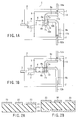
- FIG. 10A schematically shows a first example of a conventional module for the optical communications.
- a module for optical communications 101 includes a package 102 in which a light receiving element and wiring substrate described later are contained.
- a light receiving element 104 which receives a light incident from an optical fiber 103 and photoelectrically converts the light
- a wiring substrate 105 On the wiring substrate 105, there are disposed: semiconductor devices (hereinafter referred to as IC) such as a preamplifier 106 which amplifies a signal from the light receiving element 104; and wiring patterns 107a, 107b.
- IC semiconductor devices
- a differential output form has frequently been used which has a reverse and non-reverse outputs in order to enhance an SN ratio with respect to an external noise.
- a connection pad 108a formed on an upper side outputs the non-reverse output
- a connection pad 108b on a lower side outputs the reverse output.
- the wiring patterns 107a, 107b substantially have symmetric shapes in a perpendicular direction, and these wiring patterns 107a, 107b are disposed opposite to each other.
- the connection pads 108a, 108b and wiring patterns 107a, 107b are connected to each other via bonding wires 109.
- the wiring patterns 107a, 107b are connected to lead pins 110a, 110b in ends of the wiring substrate 105.
- the above-described module for optical communications 101 is disposed, for example, on a substrate, and the substrate is assembled in various apparatuses for use.
- FIG. 11 shows a second conventional example of the module for optical communications.
- a module for optical communications 121 includes the light receiving element 104 and wiring substrate 105 in the package 102.
- An IC 122 is disposed on the wiring substrate 105.
- the IC 122 includes a connection pin 123a which outputs the reverse output and a connection pin 123b which outputs the non-reverse output.
- the connection pins 123a, 123b are connected to wiring patterns 124a, 124b.
- the wiring patterns 124a, 124b are respectively connected to the lead pins 110a, 110b, for example, via bonding wires.
- the lead pin 110a is connected to the connection pad 108a to output the non-reverse output
- the lead pin 110b is connected to the connection pad 108b to output the reverse output.
- the arrangement of these lead pins is not optionally determined.
- a side on which the connection pads 108a, 108b of the IC 106 are formed does not meet with a side on which the lead pins 110a, 110b are formed. That is, the lead pin 110a forms the reverse output, and the lead pin 110b forms the non-reverse output.
- connection pad 108a forms the reverse output
- the lower connection pad 108b forms the non-reverse output. This increases costs.
- the IC with a connection pad arrangement that meets the demand of a user may not be manufactured.
- connection relations between the connection pads 108a, 108b and lead pins 110a, 110b need to be reversed.
- a method comprising: allowing the bonding wires 109 for connecting the connection pads 108a, 108b to the wiring patterns 107a, 107b to intersect with each other. That is, the connection pad 108a is connected to the wiring pattern 107b, and the connection pad 108b is connected to the wiring pattern 107a.
- connection pins 123a, 123b of the IC 122 may not be on the same side as the lead pins 110a, 110b in some cases.
- a module for optical communications comprising: a light receiving element receiving the light signal and converting the light signal to an electric signal; an insulating substrate including a first major surface and a second major surface opposite to the first major surface; an output section provided on the first major surface and extracting the electric signal as a reverse signal and non-reverse signal; first and second connection terminals connected to the output section, the reverse signal being outputted via the first connection terminal, the non-reverse signal being outputted via the second connection terminal; and first and second wiring patterns provided on the first major surface, one of the first and second wiring patterns being electrically connected to the first connection terminal, the other one of the first and second wiring patterns being electrically connected to the second connection terminal, the first wiring pattern including a first end, the second wiring pattern including a second end, and the first and second ends being provided in order in a direction intersecting with a line connecting the first and second connection terminals.
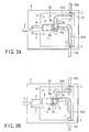
- FIG. 1A schematically shows a module for optical communications according to a first embodiment of the present invention.
- a module for optical communications 1 includes a package (envelope) 2 in which a light receiving element and wiring substrate described later are contained.
- the package 2 there are disposed: an optical fiber 3; a light receiving element 4 which receives a light signal incident from the optical fiber 3; and a wiring substrate 5 disposed adjacent to the light receiving element 4.
- the wiring substrate 5 is formed, for example, of silicon and ceramic such as alumina (Al 2 O 3 ), aluminum nitride (AlN) and silicon nitride (Si 3 N 4 ).
- an IC 6 is disposed opposite to the light receiving element 4.
- the IC 6 includes a preamplifier which is connected to the light receiving element 4 via bonding wires 7 and which amplifies a signal from the light receiving element 4 and outputs differential signals.
- the IC 6 includes a connection pad 8a which forms a non-reverse output, and a connection pad 8b which forms a reverse output.
- the connection pads (connection terminals) 8a, 8b are arranged along a side disposed opposite to a side on which, for example, the light receiving element 4 is disposed.
- wiring patterns 9a, 9b are disposed on the wiring substrate 5.
- the wiring patterns 9a, 9b are connected to the connection pads 8a, 8b via bonding wires 7a, 7b.
- Each of the wiring patterns 9a, 9b can be formed as a so-called coplanar line in which a signal electrode line is formed in a middle and ground electrodes are formed at a predetermined interval in opposite ends.
- a signal electrode line is formed in a middle and ground electrodes are formed at a predetermined interval in opposite ends.
- the respective bonding wires 7a, 7b are connected to the wiring patterns 9a, 9b. This means that the wires are connected to the signal electrode lines, unless otherwise specified.
- the coplanar line will be described later in detail.
- the wiring patterns 9a, 9b include, for example, first ends 10a, 10b, and second ends 11a, 11b and have substantially L shapes.
- the wiring patterns 9a, 9b are disposed vertically adjacent to each other.
- the upper wiring pattern 9a is disposed such that a character L is rotated in a clockwise direction by 90 degrees.
- the lower wiring pattern 9b is disposed such that the wiring pattern 9a is further rotated in a clockwise direction by 90 degrees.
- the first end 10a of the wiring pattern 9a is disposed not to contact the side on which the connection pads 8a, 8b are disposed.
- the first end 10b of the wiring pattern 9b is disposed opposite to the side on which the connection pads 8a, 8b of the IC 6 are disposed via the wiring pattern 9a in a non-contact state.
- the second ends 11a, 11b of the wiring patterns 9a, 9b are positioned in the ends of the wiring substrate 5.
- the wiring patterns 9a, 9b do not contact each other.
- the second end 11a of the wiring pattern 9a is connected to a lead pin 12a via the bonding wire 7, and the second end 11b of the wiring pattern 9b is connected to a lead pin 12b via the bonding wire 7.
- a resist 13 consisting of an insulating film such as resin is formed on the wiring pattern 9a disposed between the wiring pattern 9b and IC 6.
- the bonding wire 7a is disposed over the resist 13.
- a light signal incident from the optical fiber 3 is converted to an electric signal by the light receiving element 4.
- the electric signal converted by the light receiving element 4 is amplified by the IC 6, and outputted as non-reverse and reverse output signals to the outside of the package 2 from the lead pins 12a, 12b via the wiring patterns 9a, 9b.
- FIG. 1B schematically shows a constitution in which positions of the reverse and non-reverse outputs of the module for optical communications 1 constituted as described above are reversed, the lead pin 12a forms the reverse output, and the lead pin 12b forms the non-reverse output.
- the bonding wire 7a connected to the connection pad 8a of the non-reverse output of the IC 6 is connected to the wiring pattern 9b over the resist 13.
- the bonding wire 7b connected to the connection pad 8b of the reverse output of the IC 6 is connected to the wiring pattern 9a. Therefore, the lead pin 12a corresponds to the reverse output, and the lead pin 12b corresponds to the non-reverse output.
- FIG. 2A is a sectional view schematically showing the structure of the coplanar line.
- a signal electrode line 22 is formed substantially in a middle on a substrate 21.
- Ground electrode lines 23 are formed, for example, at a gap of about 0.1 mm on opposite sides of the signal electrode line 22.
- the substrate 21 in FIG. 2 corresponds to the wiring substrate 5 in the first embodiment shown in FIGS. 1A and 1B. FIG. 2B will be described later.
- two substantially L-shaped wiring patterns 9a, 9b are disposed on the wiring substrate 5, one end of the wiring pattern 9a is disposed adjacent to the IC 6 with a predetermined interval, and one end of the wiring pattern 9b is further disposed adjacent to one end of the wiring pattern 9a.
- the wiring patterns 9a, 9b are disposed vertically adjacent to each other with angles different from each other by 90 degrees. Therefore, a connection relation between the bonding wires 7a, 7b connecting the wiring patterns 9a, 9b to the connection pads 8a, 8b is changed, and then the disagreement of the positional relations can be adjusted.
- the bonding wires 109 do not have to intersect with each other. Therefore, it is possible to avoid short-circuiting the bonding wires 7a, 7b, and the deterioration of the frequency characteristics by the mutual inductance and parasitic capacity between the bonding wires 7a, 7b.
- the lead pins 12a, 12b can be set to desired outputs. Therefore, it is unnecessary to newly prepare the wiring substrate which satisfies the desired wiring pattern, or to separately prepare an IC in which the connection pads 8a, 8b correspond to the desired outputs. Therefore, a manufacturing cost of the module for optical communications 1 can be reduced.
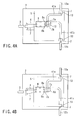
- FIG. 3A schematically shows the module for optical communications according to a second embodiment of the present invention.
- FIG. 3B schematically shows that the relation between the reverse and non-reverse outputs of the lead pins 12a, 12b of the module for optical communications shown in FIG. 3A.
- the coplanar lines in which the ground electrode is not disposed in the back surface of the wiring substrate 5 are used.
- grounded coplanar lines 31a, 31b in which the ground electrode is formed on the back surface of the wiring substrate 5 are used.
- Reference numeral 32 denotes through holes. The other parts are similar to those of the first embodiment.
- FIG. 2B schematically shows the structure of the grounded coplanar line.
- the grounded coplanar line includes a structure in which a ground electrode 24 is disposed over the back surface of the substrate 21.
- FIG. 4A schematically shows the module for optical communications according to a third embodiment of the present invention.
- FIG. 4B schematically shows that the relation between the reverse and non-reverse outputs of the lead pins 12a, 12b of the module for optical communications shown in FIG. 4A is changed.
- the wiring substrate 5 silicon, ceramic, and the like are used as the wiring substrate 5, and the coplanar line or grounded coplanar line is used as the wiring patterns 9a, 9b.
- the wiring patterns 9a, 9b wiring patterns 41a, 41b including a normal structure (micro strip structure) are used, and a material having a high permittivity is used as the wiring substrate 5.
- the material having the high permittivity include sapphire, arsenic gallium, barium titanate-based dielectric material, perovskite dielectric material, and the like.
- FIG. 5A schematically shows the module for optical communications according to a fourth embodiment of the present invention.
- a module for optical communications 51, the optical fiber 3, light receiving element 4, and wiring substrate 5 disposed adjacent to the light receiving element 4 are disposed in the package 2.
- the IC 6 such as the preamplifier is disposed opposite to the light receiving element 4.
- the connection pad 8a of the IC 6 corresponds, for example, to the non-reverse output, and the pad 8b corresponds to the reverse output.
- wiring patterns 35a, 35b are connected to connection pins 8a, 8b.
- the wiring patterns 35a, 35b includes, for example, major portions which have linear shapes. Moreover, the wiring patterns 35a, 35b are vertically disposed substantially in parallel to each other with a predetermined interval. Moreover, as described above, one part of each pattern is bent so that one end of the pattern is connected to each of the connection pins 8a, 8b of the IC 6. This bent shape may be any shape as long as one end of the wiring patterns 35a, 35b are formed so as to be connected to the connection pins 8a, 8b of the IC 6.
- Linear portions of the wiring patterns 35a, 35b have void portions 36a, 36b of the patterns substantially in the middle thereof. These portions are formed so as to be non-conductive, and thereby each pattern is separated into two parts. That is, the wiring pattern 35a includes first and second wiring patterns 35c and 35d. One end of the first wiring pattern 35c is connected to the connection pin 8a. One end of the second wiring pattern 35d is disposed opposite to the other end of the first wiring pattern 35c via the void portion 36a. Similarly, the wiring pattern 35b includes third and fourth wiring patterns 35e and 35f. One end of the third wiring pattern 35e is connected to the connection pin 8b. One end of the fourth wiring pattern 35f is disposed opposite to the other end of the third wiring pattern 35e via the void portion 36b.
- second intersecting patterns 37a, 37b are disposed between the wiring patterns 35a, 35b.
- the first wiring pattern 37a is disposed on the surface of the wiring substrate 5.
- one end of the first intersecting pattern 37a has an interval from the other end of the first wiring pattern 35c, and the other end thereof has an interval from one end of the fourth wiring pattern 35f.
- FIGS. 5B and 5C are diagrams showing one example of a section taken along the second intersecting pattern 37b of FIG. 5A. Additionally, in these drawings, the first intersecting pattern 37a is omitted. As shown in FIG. 5A, one end of the second intersecting pattern 37b has an interval from one end of the second wiring pattern 35d in the surface of the wiring substrate 5. Moreover, the other end also has an interval from the other end of the third wiring pattern 35e. Moreover, as shown in FIG.
- the connecting portion of the second intersecting pattern 37b is disposed on the back surface of the wiring substrate 5. These opposite ends and connecting portion of the second intersecting pattern are connected to one another via through holes 38 formed in the wiring substrate 5. Furthermore, as shown in FIG. 5C, the wiring substrate 5 may have a multilayered structure. In this case, the connecting portion can be disposed between the layers.
- the second and fourth wiring patterns 35d, 35f are connected to the lead pins 12a, 12b via the bonding wires 7.
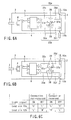
- FIGS. 6A and 6B schematically show the connected state of the wiring patterns 35a, 35b to the first and second intersecting patterns 37a, 37b in the module for optical communications 51 shown in FIG. 5A.
- a method of connecting the wiring patterns 35a, 35b to the first and second intersecting patterns 37a, 37b will be described hereinafter with reference to FIGS. 6A and 6B.
- connection patterns 39 are disposed to electrically connect the void portion 36a of the wiring pattern 35a.
- the first wiring pattern 35c is connected to the second wiring pattern 35d, and the lead pin 12a outputs the non-reverse output.
- the connection patterns 39 are disposed to electrically connect the void portion 36b of the wiring pattern 35b.
- the third wiring pattern 35e is connected to the fourth wiring pattern 35f, and the lead pin 12b outputs the reverse output.
- connection patterns 39 conductive members such as a resistor of substantially 0 ohm, wire bonding and capacitor can be used.
- the void portions 36a, 36b can be connected substantially with no resistance value with respect to an alternating signal.
- connection pattern 39 is used to connect the other end of the first wiring pattern 35c to one end of the first intersecting pattern 37a, and to connect the other end of the first intersecting pattern 37a to one end of the fourth wiring pattern 35f.
- the lead pin 12b outputs the non-reverse output.
- connection pattern 39 is used to connect one end of the second wiring pattern 35d to one end of the second intersecting pattern 37b, and to connect the other end of the second intersecting pattern 37b to the other end of the third wiring pattern 35e. In this case, the lead pin 12a outputs the reverse output.
- FIG. 6C shows a relation with a light signal and outputs from the lead pins 12a, 12b in the connection of the void portions 36a, 36b (connection non-reverse) and in the connection of the void portions via the first and second intersecting patterns 37a, 37b (connection reverse).
- connection when the connection is reversed or not reversed, the outputs of the lead pins 12a, 12b are reversed.
- the wiring pattern 35a is connected to the connection pin 8a of the IC 6, and includes the void portion 36a in the middle thereof
- the wiring pattern 35b is connected to the connection pin 8b, and includes the void portion 36b in the middle thereof.
- the first and second intersecting patterns 37a, 37b are disposed on the front and back surfaces of the wiring substrate 5 between the wiring patterns 35a, 35b.
- the connection pattern 39 is used to connect the void portions 36a, 36b, or to connect the wiring patterns 35a, 35b via the first and second intersecting patterns 37a, 37b, so that the lead pins 12a, 12b can output desired outputs.
- connection relation between the reverse and non-reverse outputs of the connection pins 8a, 8b of the IC 6 does not agree with the desired positional relation between the reverse and non-reverse outputs of the lead pins 12a, 12b, the connection relation between the reverse and non-reverse outputs can be changed so as to adjust the disagreement of the positional relation.
- the lead pins 12a, 12b can output the desired outputs. Therefore, it is unnecessary to prepare a new wiring substrate which satisfies the desired wiring pattern, or to separately prepare the IC in which the connection pins 8a, 8b output the desired outputs. This can reduce the manufacturing cost of the module for optical communications 51.
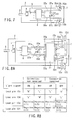
- FIG. 7 schematically shows the module for optical communications according to a fifth embodiment of the present invention.
- the portions connecting the opposite ends of the second intersecting pattern 37b are formed in the back surface or inner layer of the wiring substrate 5.
- the connecting portions include bonding wires 61 disposed on the surface of the wiring substrate 5. The other parts are similar to the fourth embodiment.
- the effect similar to that of the fourth embodiment is obtained. Moreover, when the connecting portion cannot be formed in the back surface or inner layer of the wiring substrate 5, it is easy to form the second intersecting pattern 37b.
- FIG. 8A schematically shows the module for optical communications according to a sixth embodiment of the present invention.
- an IC 71 such as a CDR IC in addition to the module for optical communications according to the fifth embodiment.
- the IC 71 outputs differential signals, which is inputted to the IC 71 or regenerated, and differential clock signals generated in response to the differential signals.
- connection pins 72c, 72d output differential signals, which are inputted to the IC 71 or regenerated, and connection pins 72e, 72f output differential signals of clock signals.
- the differential clock signals' periods are half time long of the period of the differential signals.
- Connection pins 72c to 72e are connected to lead pins 12c to 12f via wiring patterns 74 and bonding wires 7.
- FIG. 8B shows the output signals of the lead pins 12c to 12f, when the connection of the module for optical communications shown in FIG. 8A is reversed or non-reversed.
- a positive tilt indicates a signal whose edge rises in a middle point in a half cycle of the light signal
- a negative tilt indicates a signal whose edge falls in the middle point.
- the lead pins 12c, 12d can output desired outputs.
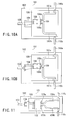
- FIG. 9A schematically shows the module for optical communications according to a seventh embodiment of the present invention.
- structures of the wiring patterns 35a, 35b and first and second intersecting patterns 37a, 37b described in the fourth embodiment are applied to an output section of the IC 71.
- connection pins 8a, 8b of the IC 6 are connected to connection pins 72a, 72b of the IC 71 via wiring patterns 81a, 81b.
- One end of wiring patterns 82a, 82b are connected to connection pins 72c, 72d of the IC 71.
- the wiring patterns 82a, 82b include non-conductive void portions, and intersecting patterns 83a, 83b are disposed between the intersecting patterns 82a, 82b.
- wiring patterns 82c, 82d are connected to connection pins 72e, 72f of the IC 71.
- the wiring patterns 82c, 82d include non-conductive void portions, and intersecting patterns 83c, 83d are disposed between the intersecting patterns 82c, 82d.
- the data signal from the IC 6 is supplied to the IC 71, and outputted via the connection pins 72c, 72d of the IC 71. Therefore, the data signals are outputted to the outside of the module via the lead pins 12c, 12d. Similarly, clock signals are outputted via connection pins 72e, 72f of the IC 71, and outputted to the outside of the module via lead pins 12e, 12f.
- FIG. 9B shows the output signals of the lead pins 12c to 12f in the reversed and non-reversed connections of the module for optical communications shown in FIG. 9A.
- FIG. 9B in the reversed and non-reversed connections of the light and clock signals, polarities of the lead pins 12c, 12d, and 12e, 12f are independently reversed.
- the seventh embodiment the effect similar to that of the fourth embodiment is obtained. Furthermore, when the wiring and intersecting patterns of the fourth embodiment are applied to the output of the IC 71, the polarities of the lead pins 12c, 12d outputting the data signals and the polarities of the lead pins 12e, 12f outputting the clock signals can independently be reversed.
- each of the wiring patterns 9a (31a, 41a), 9b (31b, 41b) has an L shape, and these patterns are disposed vertically adjacent to one another.
- the patterns are not limited to these shapes and arrangements. That is, the wiring pattern does not have to have the L shape.
- the positions of the connection pads 8a, 8b are not limited to those shown in FIG. 1.
- the wiring patterns 9a, 9b may have shapes and arrangements such that the first ends 10a (31a, 41a), 10b (31b, 41b) are disposed in order in a direction intersecting with the line connecting the connection pads 8a, 8b.
- the first and second wiring patterns 35c, 35d, and third and fourth wiring patterns 35e, 35f are not limited to the shapes and arrangements shown in FIG. 5.
- the positions of the connection pins 8a, 8b are not limited to those shown in FIG. 5, as long as the major portions of the linear shapes of the wiring patterns 35a, 35b are arranged along at least a direction intersecting with a direction connecting the connection pins 8a, 8b.
- the first and third wiring patterns 35c, 35e may slightly vertically deviate from the second and fourth wiring patterns 35d, 35f. This also applies to the fifth to seventh embodiments.
- the first and second intersecting patterns 37a, 37b are disposed on the front and back surfaces of the wiring substrate 5.
- the second intersecting pattern 37b may intersect with the first intersecting pattern 37a without contacting the pattern. That is, the patterns may intersect each other in a direction which heads from the front surface of the wiring substrate 5 to the back surfaces. This also applies to the sixth and seventh embodiments.
- the light from the optical fiber 3 is received and photoelectrically converted by the light receiving element 4, and the differential signals are outputted and amplified by the IC 6 in the constitution.
- the light signal can also be emitted to the optical fiber 3 in response to the differential signals inputted via the lead pins 12a, 12b.
- the IC 6 may drive a light emitting element, and the light emitting element which emits a light signal in response to the signal from the IC is disposed instead of the light receiving element 4.
- the wiring patterns 35d, 35f are connected to the lead pins 12a, 12b via the bonding wires 7.
- this is not limited.
- the wiring patterns 35d, 35f may also be disposed in the vicinity of the lead pins 7a, 7b and soldered/bonded to the pins.
Landscapes
- Engineering & Computer Science (AREA)
- Microelectronics & Electronic Packaging (AREA)
- Physics & Mathematics (AREA)
- Condensed Matter Physics & Semiconductors (AREA)
- Electromagnetism (AREA)
- General Physics & Mathematics (AREA)
- Computer Hardware Design (AREA)
- Power Engineering (AREA)
- Light Receiving Elements (AREA)
- Optical Couplings Of Light Guides (AREA)
- Led Devices (AREA)
- Semiconductor Lasers (AREA)
Abstract
A module for optical communications includes
a light receiving element (4) which converts the
light signal to an electric signal and an insulating
substrate (5) including first and second surfaces
opposite to each other. An output section (6) is
provided on the first surface and extracts the electric
signal as reverse and non-reverse signals. First and
second connection terminals (8a, 8b) are connected
to the output section and output the reverse and
non-reverse signals. First and second wiring patterns
(9a, 9b) are provided on the first surface. The first
and second wiring patterns are electrically connected
to one of the first and second wiring patterns and
the other one thereof. The first and second wiring
patterns have first and second ends, respectively.
The first and second ends are provided in order in
a direction intersecting with a line connecting the
first and second connection terminals.

Description
- The present invention relates to a module for optical communications, for example, which coverts a light signal to signals of a differential form and outputs the signals, or which emits the light signal in response to the inputted differential signals.
- In recent years, due to the explosive growth of communication demands brought about by the Internet, there are now strong demands for an optical communications system. In an optical communications system, a module for an optical communications for use in a light transmitter/receiver has been required to be reduced in size and cost.
- FIG. 10A schematically shows a first example of a conventional module for the optical communications. As shown in FIG. 10A, a module for
optical communications 101 includes apackage 102 in which a light receiving element and wiring substrate described later are contained. In thepackage 102, there are disposed: alight receiving element 104 which receives a light incident from anoptical fiber 103 and photoelectrically converts the light; and awiring substrate 105. On thewiring substrate 105, there are disposed: semiconductor devices (hereinafter referred to as IC) such as apreamplifier 106 which amplifies a signal from thelight receiving element 104; andwiring patterns 107a, 107b. - For an output of the
preamplifier 106, in recent years, a differential output form has frequently been used which has a reverse and non-reverse outputs in order to enhance an SN ratio with respect to an external noise. In this conventional example, for example, aconnection pad 108a formed on an upper side outputs the non-reverse output, and aconnection pad 108b on a lower side outputs the reverse output. Thewiring patterns 107a, 107b substantially have symmetric shapes in a perpendicular direction, and thesewiring patterns 107a, 107b are disposed opposite to each other. Theconnection pads wiring patterns 107a, 107b are connected to each other viabonding wires 109. Thewiring patterns 107a, 107b are connected tolead pins wiring substrate 105. - The above-described module for
optical communications 101 is disposed, for example, on a substrate, and the substrate is assembled in various apparatuses for use. - FIG. 11 shows a second conventional example of the module for optical communications. As shown in FIG. 11, a module for
optical communications 121 includes thelight receiving element 104 andwiring substrate 105 in thepackage 102. - An IC 122 is disposed on the
wiring substrate 105. The IC 122 includes aconnection pin 123a which outputs the reverse output and aconnection pin 123b which outputs the non-reverse output. Theconnection pins wiring patterns wiring patterns lead pins - Additionally, in the first conventional example, the
lead pin 110a is connected to theconnection pad 108a to output the non-reverse output, and thelead pin 110b is connected to theconnection pad 108b to output the reverse output. However, in general, the arrangement of these lead pins is not optionally determined. In some apparatus (substrate) in which the module foroptical communications 101 is assembled, a side on which theconnection pads IC 106 are formed does not meet with a side on which thelead pins lead pin 110a forms the reverse output, and thelead pin 110b forms the non-reverse output. In this case, a separate IC needs to be prepared in which theupper connection pad 108a forms the reverse output, and thelower connection pad 108b forms the non-reverse output. This increases costs. Moreover, the IC with a connection pad arrangement that meets the demand of a user may not be manufactured. - Furthermore, conversely, depending on an IC maker, different from the
aforementioned IC 106, the positions of the reverse output and non-reverse output may be reversed. Therefore, similarly, connection relations between theconnection pads lead pins - To switch the reverse and non-reverse outputs of the module for
optical communications 101 without changing the arrangement of thewiring patterns 107a, 107b, for example, as shown in FIG. 10B, a method is considered comprising: allowing thebonding wires 109 for connecting theconnection pads wiring patterns 107a, 107b to intersect with each other. That is, theconnection pad 108a is connected to thewiring pattern 107b, and theconnection pad 108b is connected to the wiring pattern 107a. - In this method, however, since the
bonding wires 109 intersect, there is a possibility of short-circuit. Moreover, since thebonding wires 109 are disposed in the vicinity of each other, a problem is deterioration of frequency properties by mutual inductance between thebonding wires 109. - Moreover, in the second conventional example, for similar reasons, the
connection pins IC 122 may not be on the same side as thelead pins new wiring substrate 105 including the wiring pattern which satisfies the condition. This not only complicates a manufacturing process of the module for optical communications but also increases costs. - According to a first aspect of the present invention, there is provided a module for optical communications comprising: a light receiving element receiving the light signal and converting the light signal to an electric signal; an insulating substrate including a first major surface and a second major surface opposite to the first major surface; an output section provided on the first major surface and extracting the electric signal as a reverse signal and non-reverse signal; first and second connection terminals connected to the output section, the reverse signal being outputted via the first connection terminal, the non-reverse signal being outputted via the second connection terminal; and first and second wiring patterns provided on the first major surface, one of the first and second wiring patterns being electrically connected to the first connection terminal, the other one of the first and second wiring patterns being electrically connected to the second connection terminal, the first wiring pattern including a first end, the second wiring pattern including a second end, and the first and second ends being provided in order in a direction intersecting with a line connecting the first and second connection terminals.
- This summary of the invention does not necessarily describe all necessary features so that the invention may also be a sub-combination of these described features.
- The invention can be more fully understood from the following detailed description when taken in conjunction with the accompanying drawings, in which:
- FIGS. 1A and 1B are diagrams schematically showing a module for optical communications according to a first embodiment of the present invention.
- FIGS. 2A and 2B are diagrams schematically showing a structure of a wiring pattern.
- FIGS. 3A and 3B are diagrams schematically showing the module for optical communications according to a second embodiment of the present invention.
- FIGS. 4A and 4B are diagrams schematically showing the module for optical communications according to a third embodiment of the present invention.
- FIG. 5A is a diagram schematically showing the module for optical communications according to a fourth embodiment of the present invention, and FIGS. 5B and 5C are diagrams showing an example of a second intersecting pattern of FIG. 5A.
- FIGS. 6A and 6B are diagrams schematically showing a connection method of the module for optical communications shown in FIG. 5A, and FIG. 6C is a diagram showing a relation between a light signal of the module of FIGS. 6A and 6B, and an output from a lead pin.
- FIG. 7 is a diagram schematically showing the module for optical communications according to a fifth embodiment of the present invention.
- FIG. 8A is a diagram schematically showing the module for optical communications according to a sixth embodiment of the present invention, and FIG. 8B is a diagram showing the relation between the light signal of the module of FIG. 8A, and the output from the lead pin.
- FIG. 9A is a diagram schematically showing the module for optical communications according to a seventh embodiment of the present invention, and FIG. 9B is a diagram showing the relation between the light signal of the module of FIG. 9A, and the output from the lead pin.
- FIGS. 10A and 10B are diagrams schematically showing a first conventional example of the module for optical communications.
- FIG. 11 is a diagram schematically showing a second conventional example of the module for optical communications.
-
- Embodiments of the present invention will be described hereinafter with reference to the drawings. Additionally, in the following description, constituting elements including substantially the same functions and constitutions are denoted with the same reference numerals, and a description will be made only if necessary.
- FIG. 1A schematically shows a module for optical communications according to a first embodiment of the present invention. As shown in FIG. 1A, a module for
optical communications 1 includes a package (envelope) 2 in which a light receiving element and wiring substrate described later are contained. In thepackage 2, there are disposed: anoptical fiber 3; alight receiving element 4 which receives a light signal incident from theoptical fiber 3; and awiring substrate 5 disposed adjacent to thelight receiving element 4. Thewiring substrate 5 is formed, for example, of silicon and ceramic such as alumina (Al2O3), aluminum nitride (AlN) and silicon nitride (Si3N4). - On the
wiring substrate 5, anIC 6 is disposed opposite to thelight receiving element 4. Examples of theIC 6 includes a preamplifier which is connected to thelight receiving element 4 viabonding wires 7 and which amplifies a signal from thelight receiving element 4 and outputs differential signals. Moreover, theIC 6 includes aconnection pad 8a which forms a non-reverse output, and aconnection pad 8b which forms a reverse output. The connection pads (connection terminals) 8a, 8b are arranged along a side disposed opposite to a side on which, for example, thelight receiving element 4 is disposed. On thewiring substrate 5,wiring patterns wiring patterns connection pads bonding wires - Each of the
wiring patterns respective bonding wires wiring patterns - The
wiring patterns second ends wiring patterns upper wiring pattern 9a is disposed such that a character L is rotated in a clockwise direction by 90 degrees. Thelower wiring pattern 9b is disposed such that thewiring pattern 9a is further rotated in a clockwise direction by 90 degrees. - The
first end 10a of thewiring pattern 9a is disposed not to contact the side on which theconnection pads first end 10b of thewiring pattern 9b is disposed opposite to the side on which theconnection pads IC 6 are disposed via thewiring pattern 9a in a non-contact state. - The second ends 11a, 11b of the
wiring patterns wiring substrate 5. Thewiring patterns - The
second end 11a of thewiring pattern 9a is connected to alead pin 12a via thebonding wire 7, and thesecond end 11b of thewiring pattern 9b is connected to alead pin 12b via thebonding wire 7. - A resist 13 consisting of an insulating film such as resin is formed on the
wiring pattern 9a disposed between thewiring pattern 9b andIC 6. Thebonding wire 7a is disposed over the resist 13. - An operation of the module for optical communications constituted as described above will be described. A light signal incident from the
optical fiber 3 is converted to an electric signal by thelight receiving element 4. The electric signal converted by thelight receiving element 4 is amplified by theIC 6, and outputted as non-reverse and reverse output signals to the outside of thepackage 2 from the lead pins 12a, 12b via thewiring patterns - FIG. 1B schematically shows a constitution in which positions of the reverse and non-reverse outputs of the module for
optical communications 1 constituted as described above are reversed, thelead pin 12a forms the reverse output, and thelead pin 12b forms the non-reverse output. As shown in FIG. 1B, thebonding wire 7a connected to theconnection pad 8a of the non-reverse output of theIC 6 is connected to thewiring pattern 9b over the resist 13. Moreover, thebonding wire 7b connected to theconnection pad 8b of the reverse output of theIC 6 is connected to thewiring pattern 9a. Therefore, thelead pin 12a corresponds to the reverse output, and thelead pin 12b corresponds to the non-reverse output. - In addition to the above-described constitution, when the widths of the
wiring patterns bonding wires wiring patterns bonding wires wiring patterns wiring patterns - However, when the widths of the
wiring patterns wiring patterns wiring patterns wiring patterns - Now the coplanar line structure will be described. FIG. 2A is a sectional view schematically showing the structure of the coplanar line. As shown in FIG. 2A, a
signal electrode line 22 is formed substantially in a middle on asubstrate 21.Ground electrode lines 23 are formed, for example, at a gap of about 0.1 mm on opposite sides of thesignal electrode line 22. When the width of thesignal electrode line 22 and the gap width are appropriately adjusted, the desired characteristic impedance is obtained. Therefore, when the gap width is set to be as narrow as possible, the desired characteristic impedance is obtained, and the width of thesignal electrode line 22 can be reduced. Additionally, thesubstrate 21 in FIG. 2 corresponds to thewiring substrate 5 in the first embodiment shown in FIGS. 1A and 1B. FIG. 2B will be described later. - According to the first embodiment, two substantially L-shaped
wiring patterns wiring substrate 5, one end of thewiring pattern 9a is disposed adjacent to theIC 6 with a predetermined interval, and one end of thewiring pattern 9b is further disposed adjacent to one end of thewiring pattern 9a. In this manner, thewiring patterns bonding wires wiring patterns connection pads - Moreover, different from the first conventional example, the
bonding wires 109 do not have to intersect with each other. Therefore, it is possible to avoid short-circuiting thebonding wires bonding wires - Furthermore, as described above, when the connection position of the
bonding wires connection pads optical communications 1 can be reduced. - FIG. 3A schematically shows the module for optical communications according to a second embodiment of the present invention. FIG. 3B schematically shows that the relation between the reverse and non-reverse outputs of the lead pins 12a, 12b of the module for optical communications shown in FIG. 3A.
- In the first embodiment, as the
wiring patterns wiring substrate 5 are used. On the other hand, in the second embodiment, groundedcoplanar lines 31a, 31b in which the ground electrode is formed on the back surface of thewiring substrate 5 are used.Reference numeral 32 denotes through holes. The other parts are similar to those of the first embodiment. - FIG. 2B schematically shows the structure of the grounded coplanar line. As shown in FIG. 2B, in addition to the structure of the coplanar line of FIG. 2A, the grounded coplanar line includes a structure in which a
ground electrode 24 is disposed over the back surface of thesubstrate 21. - Even when the grounded coplanar line is used, an effect similar to that of the first embodiment can be obtained.
- FIG. 4A schematically shows the module for optical communications according to a third embodiment of the present invention. FIG. 4B schematically shows that the relation between the reverse and non-reverse outputs of the lead pins 12a, 12b of the module for optical communications shown in FIG. 4A is changed.
- In the first and second embodiments, silicon, ceramic, and the like are used as the
wiring substrate 5, and the coplanar line or grounded coplanar line is used as thewiring patterns wiring patterns wiring patterns wiring substrate 5. Examples of the material having the high permittivity include sapphire, arsenic gallium, barium titanate-based dielectric material, perovskite dielectric material, and the like. With this constitution, thewiring patterns - According to the third embodiment, the effect similar to those of the first embodiment is obtained.
- FIG. 5A schematically shows the module for optical communications according to a fourth embodiment of the present invention. As shown in FIG. 5A, a module for
optical communications 51, theoptical fiber 3,light receiving element 4, andwiring substrate 5 disposed adjacent to thelight receiving element 4 are disposed in thepackage 2. On thewiring substrate 5, theIC 6 such as the preamplifier is disposed opposite to thelight receiving element 4. Theconnection pad 8a of theIC 6 corresponds, for example, to the non-reverse output, and thepad 8b corresponds to the reverse output. On thewiring substrate 5,wiring patterns connection pins - The
wiring patterns wiring patterns IC 6. This bent shape may be any shape as long as one end of thewiring patterns IC 6. - Linear portions of the
wiring patterns portions 36a, 36b of the patterns substantially in the middle thereof. These portions are formed so as to be non-conductive, and thereby each pattern is separated into two parts. That is, thewiring pattern 35a includes first andsecond wiring patterns first wiring pattern 35c is connected to theconnection pin 8a. One end of thesecond wiring pattern 35d is disposed opposite to the other end of thefirst wiring pattern 35c via the void portion 36a. Similarly, thewiring pattern 35b includes third andfourth wiring patterns third wiring pattern 35e is connected to theconnection pin 8b. One end of thefourth wiring pattern 35f is disposed opposite to the other end of thethird wiring pattern 35e via thevoid portion 36b. - First,
second intersecting patterns wiring patterns first wiring pattern 37a is disposed on the surface of thewiring substrate 5. Moreover, one end of thefirst intersecting pattern 37a has an interval from the other end of thefirst wiring pattern 35c, and the other end thereof has an interval from one end of thefourth wiring pattern 35f. - Opposite ends of the
second intersecting pattern 37b are disposed on the surface of thewiring substrate 5, and portions connecting the opposite ends of the pattern to each other are disposed on the back surface of thewiring substrate 5 as shown in FIGS. 5B and 5C in more detail. FIGS. 5B and 5C are diagrams showing one example of a section taken along thesecond intersecting pattern 37b of FIG. 5A. Additionally, in these drawings, thefirst intersecting pattern 37a is omitted. As shown in FIG. 5A, one end of thesecond intersecting pattern 37b has an interval from one end of thesecond wiring pattern 35d in the surface of thewiring substrate 5. Moreover, the other end also has an interval from the other end of thethird wiring pattern 35e. Moreover, as shown in FIG. 5B, the connecting portion of thesecond intersecting pattern 37b is disposed on the back surface of thewiring substrate 5. These opposite ends and connecting portion of the second intersecting pattern are connected to one another via throughholes 38 formed in thewiring substrate 5. Furthermore, as shown in FIG. 5C, thewiring substrate 5 may have a multilayered structure. In this case, the connecting portion can be disposed between the layers. - The second and
fourth wiring patterns bonding wires 7. - FIGS. 6A and 6B schematically show the connected state of the
wiring patterns second intersecting patterns optical communications 51 shown in FIG. 5A. A method of connecting thewiring patterns second intersecting patterns - As shown in FIG. 6A,
conductive connection patterns 39 are disposed to electrically connect the void portion 36a of thewiring pattern 35a. In this case, thefirst wiring pattern 35c is connected to thesecond wiring pattern 35d, and thelead pin 12a outputs the non-reverse output. Similarly, theconnection patterns 39 are disposed to electrically connect thevoid portion 36b of thewiring pattern 35b. In this case, thethird wiring pattern 35e is connected to thefourth wiring pattern 35f, and thelead pin 12b outputs the reverse output. - Additionally, as the
connection patterns 39, conductive members such as a resistor of substantially 0 ohm, wire bonding and capacitor can be used. When the capacitor is used, thevoid portions 36a, 36b can be connected substantially with no resistance value with respect to an alternating signal. - On the other hand, as shown in FIG. 6B, the
connection pattern 39 is used to connect the other end of thefirst wiring pattern 35c to one end of thefirst intersecting pattern 37a, and to connect the other end of thefirst intersecting pattern 37a to one end of thefourth wiring pattern 35f. In this case, thelead pin 12b outputs the non-reverse output. Similarly, theconnection pattern 39 is used to connect one end of thesecond wiring pattern 35d to one end of thesecond intersecting pattern 37b, and to connect the other end of thesecond intersecting pattern 37b to the other end of thethird wiring pattern 35e. In this case, thelead pin 12a outputs the reverse output. - FIG. 6C shows a relation with a light signal and outputs from the lead pins 12a, 12b in the connection of the
void portions 36a, 36b (connection non-reverse) and in the connection of the void portions via the first andsecond intersecting patterns - According to the fourth embodiment, the
wiring pattern 35a is connected to theconnection pin 8a of theIC 6, and includes the void portion 36a in the middle thereof, and thewiring pattern 35b is connected to theconnection pin 8b, and includes thevoid portion 36b in the middle thereof. Furthermore, the first andsecond intersecting patterns wiring substrate 5 between thewiring patterns connection pattern 39 is used to connect thevoid portions 36a, 36b, or to connect thewiring patterns second intersecting patterns IC 6 does not agree with the desired positional relation between the reverse and non-reverse outputs of the lead pins 12a, 12b, the connection relation between the reverse and non-reverse outputs can be changed so as to adjust the disagreement of the positional relation. - Moreover, as described above, when the connection relations of the
wiring patterns second intersecting patterns optical communications 51. - FIG. 7 schematically shows the module for optical communications according to a fifth embodiment of the present invention. In the fourth embodiment, the portions connecting the opposite ends of the
second intersecting pattern 37b are formed in the back surface or inner layer of thewiring substrate 5. On the other hand, in the fifth embodiment, the connecting portions includebonding wires 61 disposed on the surface of thewiring substrate 5. The other parts are similar to the fourth embodiment. - According to the fifth embodiment, the effect similar to that of the fourth embodiment is obtained. Moreover, when the connecting portion cannot be formed in the back surface or inner layer of the
wiring substrate 5, it is easy to form thesecond intersecting pattern 37b. - FIG. 8A schematically shows the module for optical communications according to a sixth embodiment of the present invention. In the sixth embodiment, there is further provided an
IC 71 such as a CDR IC in addition to the module for optical communications according to the fifth embodiment. TheIC 71 outputs differential signals, which is inputted to theIC 71 or regenerated, and differential clock signals generated in response to the differential signals. - As shown in FIG. 8A, one end of the
wiring patterns IC 6. The other end of the patterns are connected toconnection pins IC 71. In theIC 71, connection pins 72c, 72d output differential signals, which are inputted to theIC 71 or regenerated, andconnection pins pins 12c to 12f viawiring patterns 74 andbonding wires 7. - FIG. 8B shows the output signals of the lead pins 12c to 12f, when the connection of the module for optical communications shown in FIG. 8A is reversed or non-reversed. In FIG. 8B, a positive tilt indicates a signal whose edge rises in a middle point in a half cycle of the light signal, and a negative tilt indicates a signal whose edge falls in the middle point. As shown in FIG. 8B, with the connection reverse or non-reverse, the lead pins 12c, 12d can output desired outputs.
- According to the sixth embodiment, the effect similar to that of the fourth embodiment is obtained.
- FIG. 9A schematically shows the module for optical communications according to a seventh embodiment of the present invention. In the seventh embodiment, structures of the
wiring patterns second intersecting patterns IC 71. - As shown in FIG. 9A, the connection pins 8a, 8b of the
IC 6 are connected toconnection pins IC 71 viawiring patterns wiring patterns connection pins IC 71. Thewiring patterns intersecting patterns intersecting patterns - One end of
wiring patterns connection pins IC 71. Thewiring patterns intersecting patterns patterns - The data signal from the
IC 6 is supplied to theIC 71, and outputted via the connection pins 72c, 72d of theIC 71. Therefore, the data signals are outputted to the outside of the module via the lead pins 12c, 12d. Similarly, clock signals are outputted viaconnection pins IC 71, and outputted to the outside of the module via lead pins 12e, 12f. - FIG. 9B shows the output signals of the lead pins 12c to 12f in the reversed and non-reversed connections of the module for optical communications shown in FIG. 9A. As shown FIG. 9B, in the reversed and non-reversed connections of the light and clock signals, polarities of the lead pins 12c, 12d, and 12e, 12f are independently reversed.
- According to the seventh embodiment, the effect similar to that of the fourth embodiment is obtained. Furthermore, when the wiring and intersecting patterns of the fourth embodiment are applied to the output of the
IC 71, the polarities of the lead pins 12c, 12d outputting the data signals and the polarities of the lead pins 12e, 12f outputting the clock signals can independently be reversed. - In the first to third embodiments, each of the
wiring patterns 9a (31a, 41a), 9b (31b, 41b) has an L shape, and these patterns are disposed vertically adjacent to one another. However, the patterns are not limited to these shapes and arrangements. That is, the wiring pattern does not have to have the L shape. Moreover, the positions of theconnection pads - Concretely, the
wiring patterns connection pads - Moreover, in the fourth embodiment, the first and
second wiring patterns fourth wiring patterns wiring patterns third wiring patterns fourth wiring patterns - Moreover, in the fourth embodiment, the first and
second intersecting patterns wiring substrate 5. However, this is not limited. Thesecond intersecting pattern 37b may intersect with thefirst intersecting pattern 37a without contacting the pattern. That is, the patterns may intersect each other in a direction which heads from the front surface of thewiring substrate 5 to the back surfaces. This also applies to the sixth and seventh embodiments. - Furthermore, in the first to fifth embodiments, the light from the
optical fiber 3 is received and photoelectrically converted by thelight receiving element 4, and the differential signals are outputted and amplified by theIC 6 in the constitution. However, the light signal can also be emitted to theoptical fiber 3 in response to the differential signals inputted via the lead pins 12a, 12b. In this case, theIC 6 may drive a light emitting element, and the light emitting element which emits a light signal in response to the signal from the IC is disposed instead of thelight receiving element 4. - Moreover, in the fourth to seventh embodiments, the
wiring patterns bonding wires 7. However, this is not limited. For example, thewiring patterns
Claims (23)
- A module for optical communications, which converts a light signal to differential signals, characterized by comprising:a light receiving element (4) receiving the light signal and converting the light signal to an electric signal;an insulating substrate (5) including a first major surface and a second major surface opposite to the first major surface;an output section (6) provided on the first major surface and extracting the electric signal as a reverse signal and non-reverse signal;first and second connection terminals (8a, 8b) connected to the output section, the reverse signal being outputted via the first connection terminal, the non-reverse signal being outputted via the second connection terminal; andfirst and second wiring patterns (9a, 9b) provided on the first major surface, one of the first and second wiring patterns being electrically connected to the first connection terminal, the other one of the first and second wiring patterns being electrically connected to the second connection terminal, the first wiring pattern including a first end (10a), the second wiring pattern including a second end (10b), and the first and second ends being provided in order in a direction intersecting with a line connecting the first and second connection terminals.
- The module according to claim 1, characterized by further comprising:a package (2) covering the light receiving element (4), the substrate (5), the output section (6), the first and second connection terminals (8a, 8b), the first and second wiring patterns (9a, 9b); andlead pins (12a, 12b) projecting from the package and respectively connected to the first and second wiring patterns.
- The module according to claim 1, characterized by further comprising:an insulating film (13) provided on the first wiring pattern (9a); andconnection wires (7a, 7b) connecting the first connection terminal (8a) to the one of the first and second wiring patterns (9a, 9b) and connecting the second connection terminal (8a) to the other one of the first and second wiring patterns.
- The module according to claim 1, characterized in that each of the first and second wiring patterns (9a, 9b) comprises:a signal line (22); andground lines (23) provided at a predetermined interval on opposite sides of the signal line.
- The module according to claim 1, characterized in that the substrate essentially consists of a material selected from a group consisting of sapphire, arsenic gallium, barium titanate-based dielectric material, and perovskite dielectric material.
- A module for optical communications, which converts a light signal to differential signals, characterized by comprising:a light receiving element (4) receiving the light signal and converting the light signal to an electric signal;an insulating substrate (5) including a first major surface and a second major surface opposite to the first major surface;an output section (6) provided on the first major surface and extracting the electric signal as a reverse signal and non-reverse signal;first and second connection terminals (35c, 35e) connected to the output section, the reverse signal being outputted via the first connection terminal, the non-reverse signal being outputted via the second connection terminal;first wiring pattern (35d) provided on the first major surface, the first wiring pattern being opposite to the first connection terminal in a non-contact state;second wiring pattern (35f) provided on the first major surface, the second wiring pattern being opposite to the second connection terminal in a non-contact state;first intersecting pattern (37a) including one and end the other end, the one end being opposite to the first connection terminal in a non-contact state, the other end being opposite to the second wiring pattern in a non-contact state; andsecond intersecting pattern (37b) including one end and the other end, the one end being opposite to the second connection terminal in a non-contact state, the other end being opposite to the first wiring pattern in a non-contact state, the second intersecting pattern intersecting with the first intersecting pattern in a non-contact state in a direction heading from the first major surface to the second major surface.
- The module according to claim 6, characterized by further comprising:wherein the connection pattern (39) performs a connection selected from a group consisting of connections between the first connection terminal (35c) and the first wiring pattern (35d) and between the second connection terminal (35e) and the second wiring pattern (35f), and connections between the first connection terminal and the second wiring pattern via the first intersecting pattern (37a) and between the second connection terminal and the first wiring pattern via the second intersecting pattern (37b).a conductive connection pattern (39),
- The module according to claim 6, characterized by further comprising:a package (2) covering the light receiving element (4), the substrate (5), the output section (6), the first and second connection terminals (35c, 35e), the first and second wiring patterns (35d, 35f), the first and second intersecting patterns (37a, 37b); andlead pins (12a, 12b) projecting from the package and respectively connected to the first and second wiring patterns.
- The module according to claim 6, characterized in that the first intersecting pattern (37a) and the one and the other ends of the second intersecting pattern (37b) are provided on the first major surface, and
a portion connecting one end of the second intersecting pattern to the other end thereof is provided on the second major surface. - The module according to claim 6, characterized in that the substrate (2) comprises a multilayered structure, and
a portion connecting one end of the second intersecting pattern (37b) to the other end thereof is provided between the layers in the substrate. - The module according to claim 6, characterized in that a portion connecting one end of the second intersecting pattern (37b) to the other end thereof is a wire (61).
- The module according to claim 6, characterized by further comprising:a semiconductor device (71) including a third connection terminal (72a) connected to the first wiring pattern (35a), and a fourth connection terminal (72b) connected to the second wiring pattern (35b), the semiconductor device outputting the supplied reverse and non-reverse signals and differential clock signals.
- A module for optical communications, which converts differential signals to a light signal, characterized by comprising:an insulating substrate (5) including a first major surface and a second major surface opposite to the first major surface;first and second connection terminals (8a, 8b) respectively supplied with the reverse and non-reverse signals:an input section (6) provided on the first major surface, the input section being connected to the first and second connection terminals, and outputting an electric signal in response to the reverse and non-reverse signals;a light emitting element (4) emitting the light signal in response to the electric signal; andfirst and second wiring patterns (9a, 9b) provided on the first major surface, one of the first and second wiring patterns being electrically connected to the first connection terminal, the other one of the first and second wiring patterns being electrically connected to the second connection terminal, the first wiring pattern including a first end (10a), the second wiring pattern including a second end (10b), and the first and second ends being provided in order in a direction intersecting with a line connecting the first and second connection terminals.
- The module according to claim 13,
characterized by further comprising:a package (2) covering the light emitting element (4), the substrate (5), the input section (6), the first and second connection terminals (8a, 8b), the first and second wiring patterns (9a, 9b); andlead pins (12a, 12b) projecting from the package and respectively connected to the first and second wiring patterns. - The module according to claim 13,
characterized by further comprising:an insulating film (13) provided on the first wiring pattern (9a); andconnection wires (7a, 7b) connecting the first connection terminal (8a) to the one of the first and second wiring patterns (9a, 9b) and connecting the second connection terminal (8a) to the other one of the first and second wiring patterns. - The module according to claim 13, characterized in that each of the first and second wiring patterns (9a, 9b) comprises:a signal line (22); andground lines (23) provided at a predetermined interval on opposite sides of the signal line.
- The module according to claim 13, characterized in that the substrate essentially consists of a material selected from a group consisting of sapphire, arsenic gallium, barium titanate-based dielectric material, and perovskite dielectric material.
- A module for optical communications, which converts a light signal to differential signals, characterized by comprising:an insulating substrate (5) including a first major surface and a second major surface opposite to the first major surface;first and second connection terminals (35c, 35e) respectively supplied with the reverse and non-reverse signals:an input section (6) provided on the first major surface, the input section being connected to the first and second connection terminals, and outputting an electric signal in response to the reverse and non-reverse signals;a light emitting element (4) emitting the light signal in response to the electric signal;first wiring pattern (35d) provided on the first major surface, the first wiring pattern being opposite to the first connection terminal in a non-contact state;second wiring pattern (35f) provided on the first major surface, the second wiring pattern being opposite to the second connection terminal in a non-contact state;first intersecting pattern (37a) including one and end the other end, the one end being opposite to the first connection terminal in a non-contact state, the other end being opposite to the second wiring pattern in a non-contact state; andsecond intersecting pattern (37b) including one end and the other end, the one end being opposite to the second connection terminal in a non-contact state, the other end being opposite to the first wiring pattern in a non-contact state, the second intersecting pattern intersecting with the first intersecting pattern in a non-contact state in a direction heading from the first major surface to the second major surface.
- The module according to claim 18,
characterized by further comprising:wherein the connection pattern (39) performs a connection selected from a group consisting of connections between the first connection terminal (35c) and the first wiring pattern (35d) and between the second connection terminal (35e) and the second wiring pattern (35f), and connections between the first connection terminal and the second wiring pattern via the first intersecting pattern (37a) and between the second connection terminal and the first wiring pattern via the second intersecting pattern (37b).a conductive connection pattern (39), - The module according to claim 18, characterized by further comprising:a package (2) covering the light emitting element (4), the substrate (5), the input section (6), the first and second connection terminals (35c, 35e), the first and second wiring patterns (35d, 35f), the first and second intersecting patterns (37a, 37b); andlead pins (12a, 12b) projecting from the package and respectively connected to the first and second wiring patterns.
- The module according to claim 18, characterized in that the first intersecting pattern (37a) and the one and the other ends of the second intersecting pattern (37b) are provided on the first major surface, and
a portion connecting one end of the second intersecting pattern to the other end thereof is provided on the second major surface. - The module according to claim 18, characterized in that the substrate (2) comprises a multilayered structure, and
a portion connecting one end of the second intersecting pattern (37b) to the other end thereof is provided between the layers in the substrate. - The module according to claim 18, characterized in that a portion connecting one end of the second intersecting pattern (37b) to the other end thereof is a wire (61).
Applications Claiming Priority (2)
| Application Number | Priority Date | Filing Date | Title |
|---|---|---|---|
| JP2001287658 | 2001-09-20 | ||
| JP2001287658A JP4102043B2 (en) | 2001-09-20 | 2001-09-20 | Module for optical communication |
Publications (1)
| Publication Number | Publication Date |
|---|---|
| EP1298734A2 true EP1298734A2 (en) | 2003-04-02 |
Family
ID=19110435
Family Applications (1)
| Application Number | Title | Priority Date | Filing Date |
|---|---|---|---|
| EP02020556A Withdrawn EP1298734A2 (en) | 2001-09-20 | 2002-09-17 | Module for optical communications for converting light to differential signals |
Country Status (4)
| Country | Link |
|---|---|
| US (1) | US6794724B2 (en) |
| EP (1) | EP1298734A2 (en) |
| JP (1) | JP4102043B2 (en) |
| CN (1) | CN1405585A (en) |
Families Citing this family (6)
| Publication number | Priority date | Publication date | Assignee | Title |
|---|---|---|---|---|
| JP5127594B2 (en) * | 2008-06-26 | 2013-01-23 | 三菱電機株式会社 | Semiconductor package |
| US8556523B2 (en) * | 2010-02-03 | 2013-10-15 | Jds Uniphase Corporation | Optical transceiver with polarity inversion |
| US9033592B2 (en) * | 2012-04-13 | 2015-05-19 | Sumitomo Electric Industries, Ltd. | Optical connector module |
| JP5692143B2 (en) * | 2012-04-13 | 2015-04-01 | 住友電気工業株式会社 | Optical connector module |
| JP5692144B2 (en) * | 2012-04-13 | 2015-04-01 | 住友電気工業株式会社 | Optical connector module |
| JPWO2020196775A1 (en) * | 2019-03-28 | 2020-10-01 |
Family Cites Families (3)
| Publication number | Priority date | Publication date | Assignee | Title |
|---|---|---|---|---|
| JPH06342858A (en) | 1993-06-02 | 1994-12-13 | Sumitomo Electric Ind Ltd | Hybrid integrated circuit |
| US6285043B1 (en) | 1999-11-01 | 2001-09-04 | The Boeing Company | Application-specific optoelectronic integrated circuit |
| JP3921940B2 (en) * | 2000-12-07 | 2007-05-30 | 住友電気工業株式会社 | Optical transceiver module |
-
2001
- 2001-09-20 JP JP2001287658A patent/JP4102043B2/en not_active Expired - Fee Related
-
2002
- 2002-09-17 EP EP02020556A patent/EP1298734A2/en not_active Withdrawn
- 2002-09-17 US US10/244,941 patent/US6794724B2/en not_active Expired - Fee Related
- 2002-09-20 CN CN02142471A patent/CN1405585A/en active Pending
Also Published As
| Publication number | Publication date |
|---|---|
| JP2003101043A (en) | 2003-04-04 |
| CN1405585A (en) | 2003-03-26 |
| US6794724B2 (en) | 2004-09-21 |
| US20030052379A1 (en) | 2003-03-20 |
| JP4102043B2 (en) | 2008-06-18 |
Similar Documents
| Publication | Publication Date | Title |
|---|---|---|
| US6573600B2 (en) | Multilayer wiring substrate having differential signal wires and a general signal wire in different planes | |
| US20030058066A1 (en) | Surface acoustic wave filter device | |
| EP1160859A2 (en) | Surface-mounting type electronic circuit unit suitable for miniaturization and easy to manufacture | |
| JP6363798B2 (en) | Directional coupler and communication module | |
| JP4823648B2 (en) | Optical semiconductor device package and optical semiconductor device | |
| US10777493B2 (en) | Semiconductor device mounting board and semiconductor package | |
| JP4290314B2 (en) | High-frequency circuit, module mounted with the same, and communication device | |
| EP1303171A2 (en) | Electronic circuit unit suitable for miniaturization | |
| EP1298734A2 (en) | Module for optical communications for converting light to differential signals | |
| JP3823102B2 (en) | Optical transmission module | |
| JP5016219B2 (en) | Resonant circuit, filter circuit, and multilayer substrate | |
| US6674632B2 (en) | Mobile telephone device with passive integrated module | |
| US7196909B2 (en) | AC coupling circuit having a large capacitance and a good frequency response | |
| US6856442B2 (en) | Transmission line, optical module using the same and manufacturing method of optical module | |
| JP3895397B2 (en) | Substrate mounting method of SAW filter | |
| CN219670142U (en) | Micro-electromechanical system device | |
| WO2023189918A1 (en) | Semiconductor relay and semiconductor relay module provided with same | |
| US7449788B2 (en) | Chip structure with arrangement of side pads | |
| JP2010016196A (en) | High-frequency package | |
| JP6502826B2 (en) | Wiring board and high frequency module | |
| JP4404460B2 (en) | Multi-cavity wiring board, wiring board, multi-cavity semiconductor element storage package and semiconductor element storage package | |
| JPS60178704A (en) | Film circuit type semiconductor device | |
| JPH07234390A (en) | Method for mounting high speed optical element | |
| JPH11205074A (en) | Piezoelectric thin-film vibrator | |
| JP2541336B2 (en) | Method of connecting integrated circuit device |
Legal Events
| Date | Code | Title | Description |
|---|---|---|---|
| PUAI | Public reference made under article 153(3) epc to a published international application that has entered the european phase |
Free format text: ORIGINAL CODE: 0009012 |
|
| 17P | Request for examination filed |
Effective date: 20020917 |
|
| AK | Designated contracting states |
Kind code of ref document: A2 Designated state(s): AT BE BG CH CY CZ DE DK EE ES FI FR GB GR IE IT LI LU MC NL PT SE SK TR Designated state(s): AT BE BG CH CY CZ DE DK EE ES FI FR GB GR IE IT LI LU MC NL PT SE SK TR |
|
| AX | Request for extension of the european patent |
Extension state: AL LT LV MK RO SI |
|
| STAA | Information on the status of an ep patent application or granted ep patent |
Free format text: STATUS: THE APPLICATION HAS BEEN WITHDRAWN |
|
| 18W | Application withdrawn |
Effective date: 20050525 |