EP1286441B1 - Réseau laser à semiconducteur bi-dimensionel - Google Patents
Réseau laser à semiconducteur bi-dimensionel Download PDFInfo
- Publication number
- EP1286441B1 EP1286441B1 EP02255655A EP02255655A EP1286441B1 EP 1286441 B1 EP1286441 B1 EP 1286441B1 EP 02255655 A EP02255655 A EP 02255655A EP 02255655 A EP02255655 A EP 02255655A EP 1286441 B1 EP1286441 B1 EP 1286441B1
- Authority
- EP
- European Patent Office
- Prior art keywords
- light
- emitting device
- cooling assembly
- emitting
- dimensional light
- Prior art date
- Legal status (The legal status is an assumption and is not a legal conclusion. Google has not performed a legal analysis and makes no representation as to the accuracy of the status listed.)
- Expired - Fee Related
Links
Images


Classifications
-
- H—ELECTRICITY
- H01—ELECTRIC ELEMENTS
- H01S—DEVICES USING THE PROCESS OF LIGHT AMPLIFICATION BY STIMULATED EMISSION OF RADIATION [LASER] TO AMPLIFY OR GENERATE LIGHT; DEVICES USING STIMULATED EMISSION OF ELECTROMAGNETIC RADIATION IN WAVE RANGES OTHER THAN OPTICAL
- H01S5/00—Semiconductor lasers
- H01S5/40—Arrangement of two or more semiconductor lasers, not provided for in groups H01S5/02 - H01S5/30
- H01S5/4025—Array arrangements, e.g. constituted by discrete laser diodes or laser bar
-
- H—ELECTRICITY
- H01—ELECTRIC ELEMENTS
- H01L—SEMICONDUCTOR DEVICES NOT COVERED BY CLASS H10
- H01L2224/00—Indexing scheme for arrangements for connecting or disconnecting semiconductor or solid-state bodies and methods related thereto as covered by H01L24/00
- H01L2224/01—Means for bonding being attached to, or being formed on, the surface to be connected, e.g. chip-to-package, die-attach, "first-level" interconnects; Manufacturing methods related thereto
- H01L2224/42—Wire connectors; Manufacturing methods related thereto
- H01L2224/44—Structure, shape, material or disposition of the wire connectors prior to the connecting process
- H01L2224/45—Structure, shape, material or disposition of the wire connectors prior to the connecting process of an individual wire connector
- H01L2224/45001—Core members of the connector
- H01L2224/45099—Material
- H01L2224/451—Material with a principal constituent of the material being a metal or a metalloid, e.g. boron (B), silicon (Si), germanium (Ge), arsenic (As), antimony (Sb), tellurium (Te) and polonium (Po), and alloys thereof
- H01L2224/45138—Material with a principal constituent of the material being a metal or a metalloid, e.g. boron (B), silicon (Si), germanium (Ge), arsenic (As), antimony (Sb), tellurium (Te) and polonium (Po), and alloys thereof the principal constituent melting at a temperature of greater than or equal to 950°C and less than 1550°C
- H01L2224/45144—Gold (Au) as principal constituent
-
- H—ELECTRICITY
- H01—ELECTRIC ELEMENTS
- H01L—SEMICONDUCTOR DEVICES NOT COVERED BY CLASS H10
- H01L2224/00—Indexing scheme for arrangements for connecting or disconnecting semiconductor or solid-state bodies and methods related thereto as covered by H01L24/00
- H01L2224/01—Means for bonding being attached to, or being formed on, the surface to be connected, e.g. chip-to-package, die-attach, "first-level" interconnects; Manufacturing methods related thereto
- H01L2224/42—Wire connectors; Manufacturing methods related thereto
- H01L2224/47—Structure, shape, material or disposition of the wire connectors after the connecting process
- H01L2224/48—Structure, shape, material or disposition of the wire connectors after the connecting process of an individual wire connector
- H01L2224/4805—Shape
- H01L2224/4809—Loop shape
- H01L2224/48091—Arched
-
- H—ELECTRICITY
- H01—ELECTRIC ELEMENTS
- H01L—SEMICONDUCTOR DEVICES NOT COVERED BY CLASS H10
- H01L2224/00—Indexing scheme for arrangements for connecting or disconnecting semiconductor or solid-state bodies and methods related thereto as covered by H01L24/00
- H01L2224/01—Means for bonding being attached to, or being formed on, the surface to be connected, e.g. chip-to-package, die-attach, "first-level" interconnects; Manufacturing methods related thereto
- H01L2224/42—Wire connectors; Manufacturing methods related thereto
- H01L2224/47—Structure, shape, material or disposition of the wire connectors after the connecting process
- H01L2224/48—Structure, shape, material or disposition of the wire connectors after the connecting process of an individual wire connector
- H01L2224/484—Connecting portions
- H01L2224/48463—Connecting portions the connecting portion on the bonding area of the semiconductor or solid-state body being a ball bond
- H01L2224/48465—Connecting portions the connecting portion on the bonding area of the semiconductor or solid-state body being a ball bond the other connecting portion not on the bonding area being a wedge bond, i.e. ball-to-wedge, regular stitch
-
- H—ELECTRICITY
- H01—ELECTRIC ELEMENTS
- H01S—DEVICES USING THE PROCESS OF LIGHT AMPLIFICATION BY STIMULATED EMISSION OF RADIATION [LASER] TO AMPLIFY OR GENERATE LIGHT; DEVICES USING STIMULATED EMISSION OF ELECTROMAGNETIC RADIATION IN WAVE RANGES OTHER THAN OPTICAL
- H01S5/00—Semiconductor lasers
- H01S5/02—Structural details or components not essential to laser action
- H01S5/022—Mountings; Housings
- H01S5/0233—Mounting configuration of laser chips
- H01S5/02345—Wire-bonding
-
- H—ELECTRICITY
- H01—ELECTRIC ELEMENTS
- H01S—DEVICES USING THE PROCESS OF LIGHT AMPLIFICATION BY STIMULATED EMISSION OF RADIATION [LASER] TO AMPLIFY OR GENERATE LIGHT; DEVICES USING STIMULATED EMISSION OF ELECTROMAGNETIC RADIATION IN WAVE RANGES OTHER THAN OPTICAL
- H01S5/00—Semiconductor lasers
- H01S5/02—Structural details or components not essential to laser action
- H01S5/022—Mountings; Housings
- H01S5/0235—Method for mounting laser chips
- H01S5/02355—Fixing laser chips on mounts
- H01S5/0237—Fixing laser chips on mounts by soldering
-
- H—ELECTRICITY
- H01—ELECTRIC ELEMENTS
- H01S—DEVICES USING THE PROCESS OF LIGHT AMPLIFICATION BY STIMULATED EMISSION OF RADIATION [LASER] TO AMPLIFY OR GENERATE LIGHT; DEVICES USING STIMULATED EMISSION OF ELECTROMAGNETIC RADIATION IN WAVE RANGES OTHER THAN OPTICAL
- H01S5/00—Semiconductor lasers
- H01S5/02—Structural details or components not essential to laser action
- H01S5/024—Arrangements for thermal management
- H01S5/02407—Active cooling, e.g. the laser temperature is controlled by a thermo-electric cooler or water cooling
- H01S5/02423—Liquid cooling, e.g. a liquid cools a mount of the laser
Landscapes
- Physics & Mathematics (AREA)
- Condensed Matter Physics & Semiconductors (AREA)
- General Physics & Mathematics (AREA)
- Electromagnetism (AREA)
- Optics & Photonics (AREA)
- Semiconductor Lasers (AREA)
Claims (20)
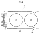
- Dispositif émetteur de lumière bi-dimensionnel comprenant :une pluralité d'unités d'émission de lumière empilées (Pn-1, Pn, Pn+1 ; Qn-1, Qn, Qn+1), chacune desdites unités d'émission de lumière ayant un ensemble de refroidissement (10) et une barre de diodes laser (60) agencée sur l'ensemble de refroidissement pour être reliée thermiquement et électriquement avec l'ensemble de refroidissement, au moins une partie (13) dudit ensemble de refroidissement (10) servant de première électrode de son unité d'émission de lumière, le dispositif étant caractérisé en ce quechacune de ladite pluralité d'unités d'émission de lumière comporte en outre une feuille de liaison automatique à bande (20) comprenant une couche électriquement conductrice (21) et une couche d'isolation (28) et agencée entre des ensembles de refroidissement adjacents (10) de telle sorte que ladite couche d'isolation est confrontée à une surface de l'ensemble de refroidissement sur laquelle la barre de diodes laser (60) est agencée, ladite couche électriquement conductrice comprenant une section d'extension nervurée (22) pour la connexion électrique avec la barre de diodes laser et servant de seconde électrode de son unité d'émission de lumière, où ladite première électrode et ladite seconde électrode sont isolées électriquement l'une de l'autre par ladite couche d'isolation (28).
- Dispositif émetteur de lumière bi-dimensionnel selon la revendication 1, où chaque ensemble de refroidissement (10) possède des ouvertures (16, 17) pour former des passages pour introduire et évacuer un agent de refroidissement et des chemins d'agent de refroidissement communiquant avec les passages, et chaque feuille de liaison automatique à bande (20) possède des ouvertures (26, 27) correspondant auxdites ouvertures ménagées dans l'ensemble de refroidissement.
- Dispositif émetteur de lumière bi-dimensionnel selon la revendication 1 ou 2, où chacune desdites unités émettrices de lumière (Pn-1, Pn, Pn+1 ; Qn-1, Qn, Qn+1) présente en outre une plaque d'écartement (31, 32) pour ajuster un espace entre des ensembles de refroidissement adjacents.
- Dispositif émetteur de lumière bi-dimensionnel selon la revendication 3, où ladite plaque d'écartement (31) est agencée entre la feuille de liaison automatique à bande (20) et la surface de l'ensemble de refroidissement (10) de son unité émettrice de lumière (Pn-1, Pn, Pn+1).
- Dispositif émetteur de lumière bi-dimensionnel selon la revendication 3 ou 4, où ladite plaque d'écartement (31, 32) est constituée par un élément qui présente une adhésion par la chaleur.
- Dispositif émetteur de lumière bi-dimensionnel selon la revendication 3, où ladite plaque d'écartement (32) est agencée entre la feuille de liaison automatique à bande (20) de son unité émettrice de lumière (Qn) et l'ensemble de refroidissement (10) de l'unité émettrice de lumière (Qn+1) adjacente à son unité émettrice de lumière.
- Dispositif émetteur de lumière bi-dimensionnel selon l'une des revendications 3 à 6, où ladite plaque d'écartement (31, 32) est réalisée en un matériau électriquement conducteur.
- Dispositif émetteur de lumière bi-dimensionnel selon la revendication 7, où ladite plaque d'écartement (31, 32) est réalisée en cuivre.
- Dispositif émetteur de lumière bi-dimensionnel selon la revendication 7, où ladite plaque d'écartement (31, 32) est réalisée en un alliage contenant du cuivre et du tungstène.
- Dispositif émetteur de lumière bi-dimensionnel selon l'une des revendications 3 à 6, où ladite plaque d'écartement (31, 32) est formée par un élément réalisé en un matériau isolant revêtu d'un matériau électriquement conducteur.
- Dispositif émetteur de lumière bi-dimensionnel selon la revendication 6, ou l'une quelconque des revendications 7 à 10 lorsqu'elles dépendent de la revendication 6, où au moins une surface de ladite plaque d'écartement (32) confrontée à la feuille de liaison automatique à bande (20) de son unité émettrice de lumière (Qn) et une surface de ladite plaque d'écartement confrontée à l'ensemble de refroidissement (10) de l'unité d'émettrice de lumière (Qn+1) adjacente à son unité émettrice de lumière sont revêtues d'une brasure.
- Dispositif émetteur de lumière bi-dimensionnel selon l'une des revendications précédentes, où ladite feuille de liaison automatique à bande (20) comprend en outre une plaque métallique agencée sur ladite couche électriquement conductrice (21).
- Dispositif émetteur de lumière bi-dimensionnel selon la revendication 12, où ladite plaque métallique est une plaque de cuivre.
- Dispositif émetteur de lumière bi-dimensionnel selon la revendication 13, où ladite plaque de cuivre est revêtue d'une brasure.
- Dispositif émetteur de lumière bi-dimensionnel selon l'une des revendications 1 à 11, où ladite feuille de liaison automatique à bande (20) comprend en outre une plaque isolante ayant une couche électriquement conductrice (21) formée sur celle-ci.
- Dispositif émetteur de lumière bi-dimensionnel selon l'une des revendications précédentes, où une portion de connexion (23) de ladite section d'extension (22) de ladite feuille de liaison automatique à bande (20) à relier électriquement à la barre de diodes laser (60) est revêtue d'une brasure ou d'or.
- Dispositif émetteur de lumière bi-dimensionnel selon l'une des revendications précédentes, où des fentes (24, 25) sont formées au voisinage d'une portion de connexion (23) de ladite section d'extension (22) de ladite feuille de liaison automatique à bande (20) pour être reliées électriquement à la barre de diodes laser (60).
- Dispositif émetteur de lumière bi-dimensionnel selon l'une des revendications précédentes, où les surfaces externes des ensembles de refroidissement (10) sont revêtues d'or.
- Dispositif émetteur de lumière bi-dimensionnel selon l'une des revendications précédentes, où chacune desdites unités émettrices de lumière (Pn-1, Pn, Pn+1 ; Qn-1, Qn, Qn+1) présente en outre une pièce d'écartement de matrice (41) placée entre la barre de diodes laser (60) et l'ensemble de refroidissement (10).
- Dispositif émetteur de lumière bi-dimensionnel selon la revendication 19, où ladite pièce d'écartement de matrice (41) est réalisée en un matériau ayant un coefficient de dilatation thermique proche d'un coefficient de dilatation thermique de la barre de diodes laser (60) et une conductivité de chaleur élevée.
Applications Claiming Priority (2)
| Application Number | Priority Date | Filing Date | Title |
|---|---|---|---|
| JP2001250314 | 2001-08-21 | ||
| JP2001250314A JP3643328B2 (ja) | 2001-08-21 | 2001-08-21 | 2次元ldアレイ発光装置 |
Publications (3)
| Publication Number | Publication Date |
|---|---|
| EP1286441A2 EP1286441A2 (fr) | 2003-02-26 |
| EP1286441A3 EP1286441A3 (fr) | 2004-01-02 |
| EP1286441B1 true EP1286441B1 (fr) | 2006-11-08 |
Family
ID=19079162
Family Applications (1)
| Application Number | Title | Priority Date | Filing Date |
|---|---|---|---|
| EP02255655A Expired - Fee Related EP1286441B1 (fr) | 2001-08-21 | 2002-08-14 | Réseau laser à semiconducteur bi-dimensionel |
Country Status (4)
| Country | Link |
|---|---|
| US (1) | US6934309B2 (fr) |
| EP (1) | EP1286441B1 (fr) |
| JP (1) | JP3643328B2 (fr) |
| DE (1) | DE60215892T2 (fr) |
Cited By (1)
| Publication number | Priority date | Publication date | Assignee | Title |
|---|---|---|---|---|
| RU2712764C1 (ru) * | 2019-06-11 | 2020-01-31 | Федеральное государственное бюджетное учреждение науки Физический институт им. П.Н. Лебедева Российской академии наук (ФИАН) | Способ создания двумерной матрицы лазерных диодов и двумерная матрица лазерных диодов |
Families Citing this family (30)
| Publication number | Priority date | Publication date | Assignee | Title |
|---|---|---|---|---|
| JP4934954B2 (ja) * | 2003-10-15 | 2012-05-23 | 日亜化学工業株式会社 | ヒートシンク及びヒートシンクを備えた半導体装置 |
| JP4654664B2 (ja) * | 2004-01-13 | 2011-03-23 | セイコーエプソン株式会社 | 光源装置および投射型表示装置 |
| JP4600733B2 (ja) * | 2004-07-12 | 2010-12-15 | ソニー株式会社 | 半導体レーザ装置およびその製造方法 |
| JP2007019265A (ja) * | 2005-07-07 | 2007-01-25 | Sony Corp | 発光装置 |
| DE102006051745B4 (de) * | 2006-09-28 | 2024-02-08 | OSRAM Opto Semiconductors Gesellschaft mit beschränkter Haftung | LED-Halbleiterkörper und Verwendung eines LED-Halbleiterkörpers |
| JP2008139279A (ja) * | 2006-11-02 | 2008-06-19 | Kyoto Denkiki Kk | 照明装置 |
| DE102007009380A1 (de) * | 2007-02-21 | 2008-09-04 | Forschungsverbund Berlin E.V. | Impulslaser und Verfahren zur Erzeugung von Laserstrahlung |
| DE102007016772A1 (de) * | 2007-04-04 | 2008-10-16 | Jenoptik Laserdiode Gmbh | Stapelbare mehrschichtige Mikrokanalwärmesenke |
| JP2008300596A (ja) * | 2007-05-31 | 2008-12-11 | Sony Corp | ヒートシンクおよび半導体レーザ装置 |
| US7623560B2 (en) * | 2007-09-27 | 2009-11-24 | Ostendo Technologies, Inc. | Quantum photonic imagers and methods of fabrication thereof |
| DE102008026229B4 (de) * | 2008-05-29 | 2012-12-27 | Jenoptik Laser Gmbh | Wärmeübertragungsvorrichtung zur doppelseitigen Kühlung eines Halbleiterbauelementes |
| DE102008036439A1 (de) * | 2008-08-05 | 2010-02-11 | Jenoptik Laserdiode Gmbh | Wärmeableitmodul mit einem Halbleiterelement und Herstellungsverfahren für ein solches Wärmeableitmodul |
| KR101622930B1 (ko) * | 2011-05-19 | 2016-05-31 | 벌시테크 리미티드 | 칩 적층 방법 |
| JP2012248812A (ja) * | 2011-05-31 | 2012-12-13 | Sumitomo Electric Ind Ltd | 半導体光集積素子の製造方法 |
| US8787414B1 (en) * | 2011-09-07 | 2014-07-22 | Science Research Laboratory, Inc. | Methods and systems for providing a low stress electrode connection |
| CN104485576A (zh) * | 2014-12-12 | 2015-04-01 | 中国工程物理研究院流体物理研究所 | 一种多芯组高功率塑封脉冲半导体激光二极管 |
| KR102406606B1 (ko) * | 2015-10-08 | 2022-06-09 | 삼성디스플레이 주식회사 | 유기 발광 소자, 이를 포함하는 유기 발광 표시 장치, 및 이의 제조 방법 |
| EP3447863B1 (fr) * | 2016-04-19 | 2021-03-31 | Panasonic Intellectual Property Management Co., Ltd. | Dispositif laser à semi-conducteur et son procédé de fabrication |
| CN106684707A (zh) * | 2017-03-13 | 2017-05-17 | 西安炬光科技股份有限公司 | 一种粘接型半导体激光器叠阵及其制备方法 |
| US11282981B2 (en) * | 2017-11-27 | 2022-03-22 | Seoul Viosys Co., Ltd. | Passivation covered light emitting unit stack |
| US11527519B2 (en) | 2017-11-27 | 2022-12-13 | Seoul Viosys Co., Ltd. | LED unit for display and display apparatus having the same |
| US10892296B2 (en) | 2017-11-27 | 2021-01-12 | Seoul Viosys Co., Ltd. | Light emitting device having commonly connected LED sub-units |
| US10892297B2 (en) | 2017-11-27 | 2021-01-12 | Seoul Viosys Co., Ltd. | Light emitting diode (LED) stack for a display |
| US10748881B2 (en) | 2017-12-05 | 2020-08-18 | Seoul Viosys Co., Ltd. | Light emitting device with LED stack for display and display apparatus having the same |
| US10886327B2 (en) | 2017-12-14 | 2021-01-05 | Seoul Viosys Co., Ltd. | Light emitting stacked structure and display device having the same |
| US11552057B2 (en) | 2017-12-20 | 2023-01-10 | Seoul Viosys Co., Ltd. | LED unit for display and display apparatus having the same |
| US11522006B2 (en) | 2017-12-21 | 2022-12-06 | Seoul Viosys Co., Ltd. | Light emitting stacked structure and display device having the same |
| US11552061B2 (en) | 2017-12-22 | 2023-01-10 | Seoul Viosys Co., Ltd. | Light emitting device with LED stack for display and display apparatus having the same |
| US11114499B2 (en) | 2018-01-02 | 2021-09-07 | Seoul Viosys Co., Ltd. | Display device having light emitting stacked structure |
| US10784240B2 (en) | 2018-01-03 | 2020-09-22 | Seoul Viosys Co., Ltd. | Light emitting device with LED stack for display and display apparatus having the same |
Family Cites Families (2)
| Publication number | Priority date | Publication date | Assignee | Title |
|---|---|---|---|---|
| US4716568A (en) * | 1985-05-07 | 1987-12-29 | Spectra Diode Laboratories, Inc. | Stacked diode laser array assembly |
| US6274391B1 (en) * | 1992-10-26 | 2001-08-14 | Texas Instruments Incorporated | HDI land grid array packaged device having electrical and optical interconnects |
-
2001
- 2001-08-21 JP JP2001250314A patent/JP3643328B2/ja not_active Expired - Fee Related
-
2002
- 2002-08-12 US US10/216,324 patent/US6934309B2/en not_active Expired - Fee Related
- 2002-08-14 DE DE60215892T patent/DE60215892T2/de not_active Expired - Fee Related
- 2002-08-14 EP EP02255655A patent/EP1286441B1/fr not_active Expired - Fee Related
Cited By (1)
| Publication number | Priority date | Publication date | Assignee | Title |
|---|---|---|---|---|
| RU2712764C1 (ru) * | 2019-06-11 | 2020-01-31 | Федеральное государственное бюджетное учреждение науки Физический институт им. П.Н. Лебедева Российской академии наук (ФИАН) | Способ создания двумерной матрицы лазерных диодов и двумерная матрица лазерных диодов |
Also Published As
| Publication number | Publication date |
|---|---|
| DE60215892D1 (de) | 2006-12-21 |
| US6934309B2 (en) | 2005-08-23 |
| JP2003060283A (ja) | 2003-02-28 |
| US20030039278A1 (en) | 2003-02-27 |
| EP1286441A3 (fr) | 2004-01-02 |
| DE60215892T2 (de) | 2007-03-01 |
| JP3643328B2 (ja) | 2005-04-27 |
| EP1286441A2 (fr) | 2003-02-26 |
Similar Documents
| Publication | Publication Date | Title |
|---|---|---|
| EP1286441B1 (fr) | Réseau laser à semiconducteur bi-dimensionel | |
| US6936855B1 (en) | Bendable high flux LED array | |
| JP4009056B2 (ja) | パワーモジュール | |
| US6498355B1 (en) | High flux LED array | |
| US7391153B2 (en) | Light emitting device provided with a submount assembly for improved thermal dissipation | |
| JP3847691B2 (ja) | 電力用半導体装置 | |
| US7985975B2 (en) | Light emitting package and light emitting package array formed by coupled electrodes | |
| US7723837B2 (en) | Semiconductor device | |
| US7058101B2 (en) | Stepped manifold array of microchannel heat sinks | |
| US5747876A (en) | Semiconductor device and semiconductor module | |
| US4719631A (en) | Conductively cooled laser diode array pumped laser | |
| EP3799229B1 (fr) | Dispositif laser à semi-conducteur | |
| US20060104565A1 (en) | Optical semiconductor module | |
| EP3159981A1 (fr) | Embase thermoconductrice, électroconductrice, isolée électriquement pour barrettes de diodes lasers | |
| KR20060134969A (ko) | 표면 장착 발광 칩 패키지 | |
| JP2005158957A (ja) | 発光装置 | |
| US20020110165A1 (en) | Method and system for cooling at least one laser diode with a cooling fluid | |
| JP2016054279A (ja) | 半導体レーザ | |
| CN110945653A (zh) | Led模块 | |
| US7026712B2 (en) | Peltier module with durable power supply lines and exothermic module with built-in cooler | |
| CN209913232U (zh) | 半导体激光泵浦源封装结构 | |
| US20070200223A1 (en) | Semiconductor device and semiconductor module therewith | |
| EP1341275B1 (fr) | Module laser | |
| JP2009246053A (ja) | フレーム板を備えたダイオード | |
| CN114530757A (zh) | 光半导体模块 |
Legal Events
| Date | Code | Title | Description |
|---|---|---|---|
| PUAI | Public reference made under article 153(3) epc to a published international application that has entered the european phase |
Free format text: ORIGINAL CODE: 0009012 |
|
| AK | Designated contracting states |
Kind code of ref document: A2 Designated state(s): AT BE BG CH CY CZ DE DK EE ES FI FR GB GR IE IT LI LU MC NL PT SE SK TR Designated state(s): AT BE BG CH CY CZ DE DK EE ES FI FR GB GR IE IT LI LU MC NL PT SE SK TR |
|
| AX | Request for extension of the european patent |
Extension state: AL LT LV MK RO SI |
|
| PUAL | Search report despatched |
Free format text: ORIGINAL CODE: 0009013 |
|
| AK | Designated contracting states |
Kind code of ref document: A3 Designated state(s): AT BE BG CH CY CZ DE DK EE ES FI FR GB GR IE IT LI LU MC NL PT SE SK TR |
|
| AX | Request for extension of the european patent |
Extension state: AL LT LV MK RO SI |
|
| RAP1 | Party data changed (applicant data changed or rights of an application transferred) |
Owner name: FANUC LTD |
|
| 17P | Request for examination filed |
Effective date: 20040628 |
|
| AKX | Designation fees paid |
Designated state(s): DE |
|
| 17Q | First examination report despatched |
Effective date: 20040901 |
|
| GRAP | Despatch of communication of intention to grant a patent |
Free format text: ORIGINAL CODE: EPIDOSNIGR1 |
|
| GRAS | Grant fee paid |
Free format text: ORIGINAL CODE: EPIDOSNIGR3 |
|
| GRAA | (expected) grant |
Free format text: ORIGINAL CODE: 0009210 |
|
| AK | Designated contracting states |
Kind code of ref document: B1 Designated state(s): DE |
|
| REF | Corresponds to: |
Ref document number: 60215892 Country of ref document: DE Date of ref document: 20061221 Kind code of ref document: P |
|
| PLBE | No opposition filed within time limit |
Free format text: ORIGINAL CODE: 0009261 |
|
| STAA | Information on the status of an ep patent application or granted ep patent |
Free format text: STATUS: NO OPPOSITION FILED WITHIN TIME LIMIT |
|
| 26N | No opposition filed |
Effective date: 20070809 |
|
| PG25 | Lapsed in a contracting state [announced via postgrant information from national office to epo] |
Ref country code: DE Free format text: LAPSE BECAUSE OF NON-PAYMENT OF DUE FEES Effective date: 20080301 |