EP1282136B1 - Method and apparatus for writing memory cells - Google Patents
Method and apparatus for writing memory cells Download PDFInfo
- Publication number
- EP1282136B1 EP1282136B1 EP02255052A EP02255052A EP1282136B1 EP 1282136 B1 EP1282136 B1 EP 1282136B1 EP 02255052 A EP02255052 A EP 02255052A EP 02255052 A EP02255052 A EP 02255052A EP 1282136 B1 EP1282136 B1 EP 1282136B1
- Authority
- EP
- European Patent Office
- Prior art keywords
- output
- voltage
- pulse
- cell
- comparator
- Prior art date
- Legal status (The legal status is an assumption and is not a legal conclusion. Google has not performed a legal analysis and makes no representation as to the accuracy of the status listed.)
- Expired - Lifetime
Links
- 230000015654 memory Effects 0.000 title claims description 53
- 238000000034 method Methods 0.000 title description 12
- 230000008859 change Effects 0.000 claims description 6
- 230000000977 initiatory effect Effects 0.000 claims description 2
- 230000004044 response Effects 0.000 claims 2
- 230000004888 barrier function Effects 0.000 description 9
- 239000004020 conductor Substances 0.000 description 9
- 230000015556 catabolic process Effects 0.000 description 6
- 230000008901 benefit Effects 0.000 description 4
- 239000012212 insulator Substances 0.000 description 4
- 238000004519 manufacturing process Methods 0.000 description 3
- 238000012544 monitoring process Methods 0.000 description 3
- 230000008569 process Effects 0.000 description 3
- 230000005641 tunneling Effects 0.000 description 3
- 230000004075 alteration Effects 0.000 description 2
- 230000007423 decrease Effects 0.000 description 2
- 230000001419 dependent effect Effects 0.000 description 2
- 230000007246 mechanism Effects 0.000 description 2
- 229910021420 polycrystalline silicon Inorganic materials 0.000 description 2
- 229920005591 polysilicon Polymers 0.000 description 2
- 238000012546 transfer Methods 0.000 description 2
- 229910017107 AlOx Inorganic materials 0.000 description 1
- 229910003321 CoFe Inorganic materials 0.000 description 1
- 229910001030 Iron–nickel alloy Inorganic materials 0.000 description 1
- 229910004205 SiNX Inorganic materials 0.000 description 1
- VYPSYNLAJGMNEJ-UHFFFAOYSA-N Silicium dioxide Chemical compound O=[Si]=O VYPSYNLAJGMNEJ-UHFFFAOYSA-N 0.000 description 1
- XUIMIQQOPSSXEZ-UHFFFAOYSA-N Silicon Chemical compound [Si] XUIMIQQOPSSXEZ-UHFFFAOYSA-N 0.000 description 1
- 229910003070 TaOx Inorganic materials 0.000 description 1
- 238000013459 approach Methods 0.000 description 1
- 230000002238 attenuated effect Effects 0.000 description 1
- 230000000295 complement effect Effects 0.000 description 1
- 229910052802 copper Inorganic materials 0.000 description 1
- 230000002950 deficient Effects 0.000 description 1
- 239000000696 magnetic material Substances 0.000 description 1
- 229910052751 metal Inorganic materials 0.000 description 1
- 239000002184 metal Substances 0.000 description 1
- 229910044991 metal oxide Inorganic materials 0.000 description 1
- 150000004706 metal oxides Chemical class 0.000 description 1
- 150000002739 metals Chemical class 0.000 description 1
- 230000002093 peripheral effect Effects 0.000 description 1
- 238000012106 screening analysis Methods 0.000 description 1
- 239000004065 semiconductor Substances 0.000 description 1
- 229910052710 silicon Inorganic materials 0.000 description 1
- 239000010703 silicon Substances 0.000 description 1
- 229910052814 silicon oxide Inorganic materials 0.000 description 1
- 239000007787 solid Substances 0.000 description 1
- 238000007619 statistical method Methods 0.000 description 1
- 239000000758 substrate Substances 0.000 description 1
Images

Classifications
-
- G—PHYSICS
- G11—INFORMATION STORAGE
- G11C—STATIC STORES
- G11C7/00—Arrangements for writing information into, or reading information out from, a digital store
-
- G—PHYSICS
- G11—INFORMATION STORAGE
- G11C—STATIC STORES
- G11C16/00—Erasable programmable read-only memories
- G11C16/02—Erasable programmable read-only memories electrically programmable
- G11C16/06—Auxiliary circuits, e.g. for writing into memory
- G11C16/34—Determination of programming status, e.g. threshold voltage, overprogramming or underprogramming, retention
- G11C16/3436—Arrangements for verifying correct programming or erasure
- G11C16/3468—Prevention of overerasure or overprogramming, e.g. by verifying whilst erasing or writing
- G11C16/3486—Circuits or methods to prevent overprogramming of nonvolatile memory cells, e.g. by detecting onset or cessation of current flow in cells and using the detector output to terminate programming
-
- G—PHYSICS
- G11—INFORMATION STORAGE
- G11C—STATIC STORES
- G11C17/00—Read-only memories programmable only once; Semi-permanent stores, e.g. manually-replaceable information cards
- G11C17/14—Read-only memories programmable only once; Semi-permanent stores, e.g. manually-replaceable information cards in which contents are determined by selectively establishing, breaking or modifying connecting links by permanently altering the state of coupling elements, e.g. PROM
- G11C17/16—Read-only memories programmable only once; Semi-permanent stores, e.g. manually-replaceable information cards in which contents are determined by selectively establishing, breaking or modifying connecting links by permanently altering the state of coupling elements, e.g. PROM using electrically-fusible links
-
- G—PHYSICS
- G11—INFORMATION STORAGE
- G11C—STATIC STORES
- G11C17/00—Read-only memories programmable only once; Semi-permanent stores, e.g. manually-replaceable information cards
- G11C17/14—Read-only memories programmable only once; Semi-permanent stores, e.g. manually-replaceable information cards in which contents are determined by selectively establishing, breaking or modifying connecting links by permanently altering the state of coupling elements, e.g. PROM
- G11C17/18—Auxiliary circuits, e.g. for writing into memory
Definitions
- This invention relates generally to an electronic memory device, and more particularly to methods and circuits for writing write-once read-many (WORM) memory devices, especially those employing write pulses.
- WORM write-once read-many
- a non-volatile memory may be write-once-read-many ("WORM") or reprogrammable.
- WORM write-once-read-many
- a WORM memory is written (programmed) once, and it is thereafter permanent for all practical purposes.
- Most WORM memories are field programmable, rather than requiring that programming be performed during manufacture. Examples of field programmable WORM memories include bipolar PROM (programmable read only memory), CMOS (complementary metal oxide semiconductor) PROM, EPROM (erasable PROM), and tunnel-junction based ROM.
- WORM memories are programmed by applying a relatively large voltage to selected cells in order to alter the physical characteristics of the selected cells.
- the alteration mechanism depends upon the type of memory.
- a unit memory cell of a bipolar or CMOS PROM typically consists of one transistor in series with a fuse and/or an anti-fuse, and a PROM is programmed by applying a large voltage across the fuse or anti-fuse of the selected cells.
- the applied voltage causes the fuse to open or the anti-fuse to short (or both if both are present).
- the resistance across the cell is altered, and a reading operation can detect the alteration, as contrasted with the unaltered state, by applying a small read voltage to the cell and sensing the current flowing through the cell.
- a unit memory cell of a EPROM typically consists of a transistor and a floating gate, and an EPROM is programmed by applying a large potential to transfer charge from the silicon substrate to the floating gate of selected cells.
- the mechanism for the charge transfer in this case is Fowler-Nordheim electron tunneling.
- the anti-fuse tunnel junction 100 includes a bottom electrode 120, an insulator barrier layer 140 and a top electrode 160.
- the bottom electrode 120 and the top electrode 160 could be conductor metals such as Cu, Al or the like or magnetic materials such as NiFe, CoFe, NiFeCo or the like.
- the insulator barrier layer 140 is typically very thin, from 5 ⁇ (Angstroms) to 100 ⁇ . Generally, the insulator barrier layer 140 is made of TaO x , AlO x , SiO x , SiN x , AlN x or the like.
- the thin insulator barrier allows quantum mechanical tunneling to occur and a current flows from one electrode, across the barrier layer 140, to the other electrode.
- the resistance of the tunnel junction is exponentially dependent on the thickness of the barrier layer. Therefore, by controlling the thickness during manufacturing, the tunnel junction can be made to a desired resistance value that is suitable for a particular application.
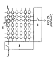
- a circuit for programming a generic WORM memory is part of a WORM memory system 200 illustrated in Figure 2A.
- the WORM memory system 200 comprises an array of memory cells 210.
- the memory cells 210 are preferably set in a rectangular arrangement of rows and columns. Each memory cell 210 is at the intersection of a row conductor 220 and a column conductor 230.
- a row decoder 240 connects to the row conductors 220, and a column decoder 250 connects to the column conductors 230.
- Address lines (not shown) control the row decoder 240 and/or the column decoder 250 to select a desired row, column or individual cell 210.
- one particular cell 110 has been selected for writing.
- a write voltage V WR is applied across the cell 210.
- a graph 260 of the write voltage V WR is illustrated in Figure 2B.
- the write voltage V WR is a pulse 270 of height V 1 and fixed width T 1 . For every cell 210 to be written, that cell 210 is selected through the row decoder 240 and the column decoder 250; then, the same pulse 270 is applied to the selected cell(s).
- V 1 is typically required to be a high value to program the memories.
- an EPROM a high voltage is needed for Fowler-Nordheim electron tunneling to occur.
- PROM with a polysilicon fuse as the programmable element, a large voltage is needed to deliver enough energy to blow the polysilicon fuse.
- a bipolar PROM with one forward and one reversed diode as a memory cell a large voltage is needed to exceed the reverse voltage of the diode to cause it to breakdown.
- the breakdown voltage of the tunnel junction is as low as 1.5 V (volts). This breakdown voltage can be controlled by the thickness of the barrier layer of the tunnel junction. A thicker barrier has a higher breakdown voltage, and a thinner barrier has a lower breakdown voltage, but these types of anti-fuse junctions exhibit significant variations in breakdown voltage.
- the programming of some WORM memories exhibit significant variability from cell to cell in the required writing voltage level. This variation can result from physical variation from cell to cell in the manufacturing process. Some cells may require less energy to be programmed, while other cells may require more. In other words, the pulse 270 may be longer than necessary for some cells yet too short for other cells. To increase yield rates, the pulse duration T 1 is typically much longer than necessary for the vast majority of cells.
- US-A-5,684,732 discloses a circuit for supplying writing currents to antifuses comprising a current generator, a switch on the write line and a comparator which compares the writing input voltage with a reference voltage. The output of the comparator controls a switching network.
- the disclosure of this document corresponds generally to the preamble of claim 1.
- the terms “has,” “have” and “having” are open-ended.
- the pulse train generator may comprise other signal interfaces besides the output referred to above.
- the term “connected”, as used herein, means connected directly or indirectly through an intermediary element.
- embodiments of the invention have the advantages that the writing process utilizes less power and the writing time is reduced, and certain embodiments of the invention are capable of achieving certain advantages, including some or all of the following: (1) the writing process is more reliable; (2) elements in series with the memory cell (e.g. row and column decoders) are less likely to be damaged; and (3) no cross connections from the array outputs are needed, as all relevant circuitry is on only the writing side of the array.
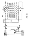
- FIG 3A illustrates a WORM memory system 300, including a circuit for programming the memory, according to an embodiment of the invention.
- the WORM memory system 300 comprises the same basic WORM memory as illustrated in Figure 2A. However, the WORM memory system 300 comprises a different circuit for programming the memory.
- the programming circuit applies a limited pulse to the memory cell 210. Preferably, the limited pulse is a two-tier pulse.
- the programming circuit monitors when the writing operation is effective, so that unnecessary expenditure of energy and time is reduced.
- the programming circuit includes a pulse generator 310, which connects (indirectly) to a write line for the selected memory cell 210.
- the write line in this case is the row conductor 220 or a line connectable (directly or indirectly) to the row conductor 220 via the row decoder 240.
- the labels "row” and “column” are arbitrary except as relative to each other. Therefore, in general, the write line could be the column conductor 230 or a line connectable to the column conductor 230 via the column decoder 250.
- the pulse generator 310 includes current source circuitry. In another embodiment, the pulse generator 310 includes voltage source circuitry with peripheral circuitry to generate a rectangular pulse at the desired pulse width, frequency and amplitude.
- the output of the pulse generator 310 connects to the drain terminal of a transistor 320.
- the source terminal of the transistor 320 connects to a resistor R 1 and a resistor R 2 in series.
- the resistor R 2 connects to the row decoder 240.
- the gate terminal of the transistor 320 is an enable input. When the voltage at the gate terminal is high, the transistor 320 conducts from drain to source, allowing the pulse generator 310 output to reach the memory cell 210 (assuming the row decoder 240 and the column decoder 250 are configured to select the memory cell 210). When the voltage at the gate terminal is low, the transistor 320 "turns off" (i.e., is open between the source and drain). In alternative embodiments, the transistor 320 can be substituted by any general switch.
- a node 325 which connects to an input of a voltage comparator 330.
- the other input of the voltage comparator 330 is connected to a reference voltage V REF .
- the output of the voltage comparator 330 is high when the voltage on the node 325 exceeds V REF ; otherwise, the output of the voltage comparator 230 is low.
- the output of the voltage comparator 330 is connected to the clock input of an SR flip-flop 335 and input of the controller 355.
- the output of the voltage comparator 330 changes from high to low and causes the Q output of the SR flip-flop 335 to turn off the transistor 320.
- the controller 355 also senses the change at the node 325 via the voltage comparator 330 and, in turn, shuts off the pulse generator 310 output on the write line for the memory cell 210.
- the controller 355 turns off the pulse generator 310 and brings the gate of the transistor 320 to a low state via the R terminal of the SR flip-flop 335.
- the slew rate of the voltage comparator 330 is preferably fast enough to detect the change in voltage at the node 325 so that the circuitry can respond in an appropriate manner with little delay.
- the resistors R 1 and R 2 act as a voltage divider. Preferably, both R 1 and R 2 are small resistors, so that the write pulse is not too severely attenuated.
- R 1 and R 2 can choose R 1 and R 2 for proper operation in conjunction with the comparator 330, the memory cell 210 and the other circuitry of the memory system 300.
- the voltage divider formed by R, and R 2 could be replaced by a current shunting arrangement, and the voltage comparator 330 could be replaced by a current comparator (connected to a reference current I REF , rather than a reference voltage V REF ).
- a current comparator connected to a reference current I REF , rather than a reference voltage V REF .
- Such an alternative circuit can detect current changes on the input side of the memory cell 210 as a result of successful writing of the cell 210. The details of such an alternative is within the ordinary skill in the art.
- Figure 3B is a graph 360 of an effective write voltage pulse 370 and an ineffective write voltage pulse 380, both for use in the programming circuit of Figure 3A.
- the effective write voltage pulse 370 illustrated as a "Utah" shaped pulse with solid outline, is the voltage at the node 325 in the case when the memory cell 210 is written successfully.
- the effective write voltage pulse 370 is a two-tier pulse of height V 21 for an interval T 21 then height V 22 for an interval T 22.
- the overall width of the effective write voltage pulse 370 is T 21 + T 22 , which is a variable, is preferably much narrower than T 1 , the width of the conventional write pulse 270 ( Figure 2B).
- the interval T 21 is the time required for writing a cell to complete.
- the interval T 22 is the time required for the circuitry to respond in this way.
- the interval T 22 is preferably as short as possible. In a best case, only enough pulse energy necessary to write a cell is applied to the cell and then quickly turned off. In this way, the effective write voltage pulse 370 is most often shorter (usually considerably shorter) than the conventional write pulse 270. Because the interval T 21 can vary from cell to cell, different length pulses may be applied to different memory cells. In this way, the programming circuit of Figure 3A self-adjusts to each cell.
- the ineffective write voltage pulse 380 shown as a rectangular pulse partially in dashed outline, is the voltage at the node 325 when an attempt to write the memory cell 210 is unsuccessful.
- the controller 355 disables the pulse after a predetermined time T 2 , which is a time that with a certain high probability would be sufficient to write the memory cell 210, if it were not defective.
- the predetermined time T 2 is an upper limit on the maximum duration of any writing operation.
- V 21 , V 22 , V REF and T 2 are dependent upon the physics of the memory cell 110.
- the voltage V 21 should carry sufficient energy to effectuate writing, but not so much energy that other circuitry (e.g., the row decoder 240 or the column decoder 250) is damaged.
- the reference voltage V REF is chosen to be some value between V 21 and V 22 (i.e., V 21 ⁇ V REF ⁇ V 22 ). Given a particular memory cell 110, one skilled in the art can pick suitable values for V 21 , V 22 (and thus R 1 and R 2 ) and T 2 . Given V 21 and V 22 , V REF can be suitably chosen.
- pulses 370 and 380 are illustrated in Figure 3B as having perfectly square edges, that is an ideal form.
- the pulses 370 and 380 typically have exponential rises and falls between levels. In fact, in full generality, the shape of the pulses is arbitrary. The multiple levels, if any, of the pulse 370 merely represent different energy levels.
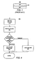
- FIG. 4 is a flow chart of a method 400, according to an embodiment of the invention.
- the method 400 selects 410 one or more cells (e.g., an entire row) to be written.
- the method 400 initiates 420 a pulse to the selected cell(s).
- the initiating step 420 turns on the pulse 370 or a similar pulse.
- the method 400 monitors 430 whether the writing has been successful or not.
- the monitoring step 430 is preferably performed by monitoring the input side of the cell, rather than sensing the cell output. If and when the writing is successful, then the method 400 optionally logs 440 the fact that the write was successful and/or the duration of the pulse.
- the duration is a measure of the quality of the cell and of the memory system generally.
- the logged data may be used at a later time for device screening or statistical analysis. If the writing is not successful according to the monitoring step 430, then the pulse has timed-out and the method 400 optionally logs 460 a failure to write the cell.
Landscapes
- Read Only Memory (AREA)
- Semiconductor Memories (AREA)
- Static Random-Access Memory (AREA)
Applications Claiming Priority (2)
| Application Number | Priority Date | Filing Date | Title |
|---|---|---|---|
| US09/917,882 US6434060B1 (en) | 2001-07-31 | 2001-07-31 | Write pulse limiting for worm storage device |
| US917882 | 2001-07-31 |
Publications (2)
| Publication Number | Publication Date |
|---|---|
| EP1282136A1 EP1282136A1 (en) | 2003-02-05 |
| EP1282136B1 true EP1282136B1 (en) | 2007-09-12 |
Family
ID=25439461
Family Applications (1)
| Application Number | Title | Priority Date | Filing Date |
|---|---|---|---|
| EP02255052A Expired - Lifetime EP1282136B1 (en) | 2001-07-31 | 2002-07-18 | Method and apparatus for writing memory cells |
Country Status (7)
Families Citing this family (15)
| Publication number | Priority date | Publication date | Assignee | Title |
|---|---|---|---|---|
| US6534841B1 (en) * | 2001-12-14 | 2003-03-18 | Hewlett-Packard Company | Continuous antifuse material in memory structure |
| JP4772328B2 (ja) * | 2005-01-13 | 2011-09-14 | 株式会社東芝 | 不揮発性半導体記憶装置 |
| JP4974588B2 (ja) * | 2005-06-01 | 2012-07-11 | 株式会社半導体エネルギー研究所 | 情報管理方法及び情報管理システム |
| US7453755B2 (en) * | 2005-07-01 | 2008-11-18 | Sandisk 3D Llc | Memory cell with high-K antifuse for reverse bias programming |
| TWI430275B (zh) * | 2008-04-16 | 2014-03-11 | Magnachip Semiconductor Ltd | 用於程式化非揮發性記憶體裝置之方法 |
| US8395923B2 (en) * | 2008-12-30 | 2013-03-12 | Intel Corporation | Antifuse programmable memory array |
| JP2010267368A (ja) * | 2009-04-17 | 2010-11-25 | Semiconductor Energy Lab Co Ltd | 半導体記憶装置 |
| JP5466594B2 (ja) * | 2010-07-29 | 2014-04-09 | ルネサスエレクトロニクス株式会社 | 半導体記憶装置及びアンチヒューズのプログラム方法 |
| US8866121B2 (en) | 2011-07-29 | 2014-10-21 | Sandisk 3D Llc | Current-limiting layer and a current-reducing layer in a memory device |
| US8659001B2 (en) | 2011-09-01 | 2014-02-25 | Sandisk 3D Llc | Defect gradient to boost nonvolatile memory performance |
| US8637413B2 (en) | 2011-12-02 | 2014-01-28 | Sandisk 3D Llc | Nonvolatile resistive memory element with a passivated switching layer |
| US8698119B2 (en) | 2012-01-19 | 2014-04-15 | Sandisk 3D Llc | Nonvolatile memory device using a tunnel oxide as a current limiter element |
| US8686386B2 (en) | 2012-02-17 | 2014-04-01 | Sandisk 3D Llc | Nonvolatile memory device using a varistor as a current limiter element |
| CN102810635A (zh) * | 2012-08-09 | 2012-12-05 | 清华大学 | 一写多读式存储器件及其制造方法 |
| US20140241031A1 (en) | 2013-02-28 | 2014-08-28 | Sandisk 3D Llc | Dielectric-based memory cells having multi-level one-time programmable and bi-level rewriteable operating modes and methods of forming the same |
Citations (1)
| Publication number | Priority date | Publication date | Assignee | Title |
|---|---|---|---|---|
| EP1278203A1 (en) * | 2001-07-20 | 2003-01-22 | Hewlett-Packard Company | Method and apparatus for writing a memory device |
Family Cites Families (14)
| Publication number | Priority date | Publication date | Assignee | Title |
|---|---|---|---|---|
| JPS6382534A (ja) * | 1986-09-26 | 1988-04-13 | Matsushita Electric Ind Co Ltd | メモリ保護装置 |
| US5008855A (en) * | 1989-07-18 | 1991-04-16 | Actel Corporation | Method of programming anti-fuse element |
| JPH03142779A (ja) * | 1989-10-27 | 1991-06-18 | Nec Corp | センスアンプ駆動回路 |
| US5257225A (en) * | 1992-03-12 | 1993-10-26 | Micron Technology, Inc. | Method for programming programmable devices by utilizing single or multiple pulses varying in pulse width and amplitude |
| US5502395A (en) * | 1994-05-25 | 1996-03-26 | Allen; William J. | Method for programming antifuses for reliable programmed links |
| US5684732A (en) * | 1995-03-24 | 1997-11-04 | Kawasaki Steel Corporation | Semiconductor devices |
| JPH1166862A (ja) * | 1997-08-14 | 1999-03-09 | Nec Corp | 半導体メモリ |
| TW387086B (en) * | 1998-05-18 | 2000-04-11 | Winbond Electronics Corp | Pulsed word-line control circuit for memory device and its controlling method |
| US6052325A (en) * | 1998-05-22 | 2000-04-18 | Micron Technology, Inc. | Method and apparatus for translating signals |
| DE19824524C2 (de) * | 1998-06-02 | 2002-08-08 | Honeywell Bv | Regeleinrichtung für Gasbrenner |
| JP2000057772A (ja) * | 1998-08-12 | 2000-02-25 | Nec Corp | 半導体記憶装置 |
| KR100371022B1 (ko) * | 1998-11-26 | 2003-07-16 | 주식회사 하이닉스반도체 | 다중비트 메모리셀의 데이터 센싱장치 |
| DE69937559T2 (de) * | 1999-09-10 | 2008-10-23 | Stmicroelectronics S.R.L., Agrate Brianza | Nicht-flüchtige Speicher mit Erkennung von Kurzschlüssen zwischen Wortleitungen |
| US6144606A (en) * | 1999-10-14 | 2000-11-07 | Advanced Micro Devices, Inc. | Method and system for bi-directional voltage regulation detection |
-
2001
- 2001-07-31 US US09/917,882 patent/US6434060B1/en not_active Expired - Lifetime
-
2002
- 2002-05-30 TW TW091111536A patent/TWI223269B/zh not_active IP Right Cessation
- 2002-07-18 DE DE60222349T patent/DE60222349D1/de not_active Expired - Lifetime
- 2002-07-18 EP EP02255052A patent/EP1282136B1/en not_active Expired - Lifetime
- 2002-07-24 JP JP2002214851A patent/JP2003123496A/ja active Pending
- 2002-07-30 KR KR1020020044798A patent/KR20030011671A/ko not_active Ceased
- 2002-07-31 CN CNB021272859A patent/CN1331153C/zh not_active Expired - Lifetime
Patent Citations (1)
| Publication number | Priority date | Publication date | Assignee | Title |
|---|---|---|---|---|
| EP1278203A1 (en) * | 2001-07-20 | 2003-01-22 | Hewlett-Packard Company | Method and apparatus for writing a memory device |
Also Published As
| Publication number | Publication date |
|---|---|
| DE60222349D1 (de) | 2007-10-25 |
| US6434060B1 (en) | 2002-08-13 |
| CN1331153C (zh) | 2007-08-08 |
| CN1400605A (zh) | 2003-03-05 |
| KR20030011671A (ko) | 2003-02-11 |
| TWI223269B (en) | 2004-11-01 |
| EP1282136A1 (en) | 2003-02-05 |
| JP2003123496A (ja) | 2003-04-25 |
Similar Documents
| Publication | Publication Date | Title |
|---|---|---|
| EP1282136B1 (en) | Method and apparatus for writing memory cells | |
| JP4264432B2 (ja) | プログラム可能な抵抗メモリ素子のプログラミング | |
| EP1278203B1 (en) | Method and apparatus for writing a memory device | |
| US6928022B2 (en) | Write driver circuit in phase change memory device and method for applying write current | |
| US6862213B2 (en) | Semiconductor memory device and control method thereof | |
| US7706178B2 (en) | Programmable matrix array with phase-change material | |
| CN101872647B (zh) | 一次编程电阻随机存储单元、阵列、存储器及其操作方法 | |
| US7646630B2 (en) | Programmable matrix array with chalcogenide material | |
| JP5297525B2 (ja) | 不揮発性記憶における同時書込みと検証 | |
| US10783961B2 (en) | Memory cells, memory systems, and memory programming methods | |
| US9646692B1 (en) | Programming verify for nonvolatile memory | |
| US20050122768A1 (en) | Nonvolatile semiconductor memory device | |
| US20060097342A1 (en) | Programmable matrix array with phase-change material | |
| JPH05266682A (ja) | トランジスター・スナップ・バックによるアンチ・ヒューズ・プログラミング | |
| US8248836B2 (en) | Non-volatile memory cell stack with dual resistive elements | |
| US7420850B2 (en) | Method for controlling current during programming of memory cells | |
| US6909638B2 (en) | Non-volatile memory having a bias on the source electrode for HCI programming | |
| US11735257B2 (en) | Memory with high-accuracy reference-free multi-inverter sense circuit and associated sensing method |
Legal Events
| Date | Code | Title | Description |
|---|---|---|---|
| PUAI | Public reference made under article 153(3) epc to a published international application that has entered the european phase |
Free format text: ORIGINAL CODE: 0009012 |
|
| AK | Designated contracting states |
Designated state(s): AT BE BG CH CY CZ DE DK EE ES FI FR GB GR IE IT LI LU MC NL PT SE SK TR |
|
| AX | Request for extension of the european patent |
Extension state: AL LT LV MK RO SI |
|
| 17P | Request for examination filed |
Effective date: 20030616 |
|
| 17Q | First examination report despatched |
Effective date: 20030724 |
|
| AKX | Designation fees paid |
Designated state(s): DE FR GB |
|
| GRAP | Despatch of communication of intention to grant a patent |
Free format text: ORIGINAL CODE: EPIDOSNIGR1 |
|
| GRAS | Grant fee paid |
Free format text: ORIGINAL CODE: EPIDOSNIGR3 |
|
| GRAA | (expected) grant |
Free format text: ORIGINAL CODE: 0009210 |
|
| AK | Designated contracting states |
Kind code of ref document: B1 Designated state(s): DE FR GB |
|
| REG | Reference to a national code |
Ref country code: GB Ref legal event code: FG4D |
|
| REF | Corresponds to: |
Ref document number: 60222349 Country of ref document: DE Date of ref document: 20071025 Kind code of ref document: P |
|
| PLBE | No opposition filed within time limit |
Free format text: ORIGINAL CODE: 0009261 |
|
| STAA | Information on the status of an ep patent application or granted ep patent |
Free format text: STATUS: NO OPPOSITION FILED WITHIN TIME LIMIT |
|
| PG25 | Lapsed in a contracting state [announced via postgrant information from national office to epo] |
Ref country code: DE Free format text: LAPSE BECAUSE OF FAILURE TO SUBMIT A TRANSLATION OF THE DESCRIPTION OR TO PAY THE FEE WITHIN THE PRESCRIBED TIME-LIMIT Effective date: 20071213 |
|
| 26N | No opposition filed |
Effective date: 20080613 |
|
| REG | Reference to a national code |
Ref country code: GB Ref legal event code: 732E Free format text: REGISTERED BETWEEN 20110203 AND 20110209 |
|
| REG | Reference to a national code |
Ref country code: FR Ref legal event code: TP |
|
| REG | Reference to a national code |
Ref country code: FR Ref legal event code: PLFP Year of fee payment: 15 |
|
| REG | Reference to a national code |
Ref country code: FR Ref legal event code: PLFP Year of fee payment: 16 |
|
| REG | Reference to a national code |
Ref country code: FR Ref legal event code: PLFP Year of fee payment: 17 |
|
| PGFP | Annual fee paid to national office [announced via postgrant information from national office to epo] |
Ref country code: FR Payment date: 20210611 Year of fee payment: 20 |
|
| PGFP | Annual fee paid to national office [announced via postgrant information from national office to epo] |
Ref country code: GB Payment date: 20210623 Year of fee payment: 20 |
|
| REG | Reference to a national code |
Ref country code: GB Ref legal event code: PE20 Expiry date: 20220717 |
|
| PG25 | Lapsed in a contracting state [announced via postgrant information from national office to epo] |
Ref country code: GB Free format text: LAPSE BECAUSE OF EXPIRATION OF PROTECTION Effective date: 20220717 |