EP1271636A1 - Thermal oxidation process control by controlling oxidation agent partial pressure - Google Patents
Thermal oxidation process control by controlling oxidation agent partial pressure Download PDFInfo
- Publication number
- EP1271636A1 EP1271636A1 EP01115213A EP01115213A EP1271636A1 EP 1271636 A1 EP1271636 A1 EP 1271636A1 EP 01115213 A EP01115213 A EP 01115213A EP 01115213 A EP01115213 A EP 01115213A EP 1271636 A1 EP1271636 A1 EP 1271636A1
- Authority
- EP
- European Patent Office
- Prior art keywords
- oxygen
- reaction chamber
- feed
- oxidising
- partial pressure
- Prior art date
- Legal status (The legal status is an assumption and is not a legal conclusion. Google has not performed a legal analysis and makes no representation as to the accuracy of the status listed.)
- Withdrawn
Links
Images

Classifications
-
- C—CHEMISTRY; METALLURGY
- C30—CRYSTAL GROWTH
- C30B—SINGLE-CRYSTAL GROWTH; UNIDIRECTIONAL SOLIDIFICATION OF EUTECTIC MATERIAL OR UNIDIRECTIONAL DEMIXING OF EUTECTOID MATERIAL; REFINING BY ZONE-MELTING OF MATERIAL; PRODUCTION OF A HOMOGENEOUS POLYCRYSTALLINE MATERIAL WITH DEFINED STRUCTURE; SINGLE CRYSTALS OR HOMOGENEOUS POLYCRYSTALLINE MATERIAL WITH DEFINED STRUCTURE; AFTER-TREATMENT OF SINGLE CRYSTALS OR A HOMOGENEOUS POLYCRYSTALLINE MATERIAL WITH DEFINED STRUCTURE; APPARATUS THEREFOR
- C30B29/00—Single crystals or homogeneous polycrystalline material with defined structure characterised by the material or by their shape
- C30B29/02—Elements
- C30B29/06—Silicon
-
- C—CHEMISTRY; METALLURGY
- C23—COATING METALLIC MATERIAL; COATING MATERIAL WITH METALLIC MATERIAL; CHEMICAL SURFACE TREATMENT; DIFFUSION TREATMENT OF METALLIC MATERIAL; COATING BY VACUUM EVAPORATION, BY SPUTTERING, BY ION IMPLANTATION OR BY CHEMICAL VAPOUR DEPOSITION, IN GENERAL; INHIBITING CORROSION OF METALLIC MATERIAL OR INCRUSTATION IN GENERAL
- C23C—COATING METALLIC MATERIAL; COATING MATERIAL WITH METALLIC MATERIAL; SURFACE TREATMENT OF METALLIC MATERIAL BY DIFFUSION INTO THE SURFACE, BY CHEMICAL CONVERSION OR SUBSTITUTION; COATING BY VACUUM EVAPORATION, BY SPUTTERING, BY ION IMPLANTATION OR BY CHEMICAL VAPOUR DEPOSITION, IN GENERAL
- C23C8/00—Solid state diffusion of only non-metal elements into metallic material surfaces; Chemical surface treatment of metallic material by reaction of the surface with a reactive gas, leaving reaction products of surface material in the coating, e.g. conversion coatings, passivation of metals
- C23C8/06—Solid state diffusion of only non-metal elements into metallic material surfaces; Chemical surface treatment of metallic material by reaction of the surface with a reactive gas, leaving reaction products of surface material in the coating, e.g. conversion coatings, passivation of metals using gases
- C23C8/08—Solid state diffusion of only non-metal elements into metallic material surfaces; Chemical surface treatment of metallic material by reaction of the surface with a reactive gas, leaving reaction products of surface material in the coating, e.g. conversion coatings, passivation of metals using gases only one element being applied
- C23C8/10—Oxidising
-
- C—CHEMISTRY; METALLURGY
- C30—CRYSTAL GROWTH
- C30B—SINGLE-CRYSTAL GROWTH; UNIDIRECTIONAL SOLIDIFICATION OF EUTECTIC MATERIAL OR UNIDIRECTIONAL DEMIXING OF EUTECTOID MATERIAL; REFINING BY ZONE-MELTING OF MATERIAL; PRODUCTION OF A HOMOGENEOUS POLYCRYSTALLINE MATERIAL WITH DEFINED STRUCTURE; SINGLE CRYSTALS OR HOMOGENEOUS POLYCRYSTALLINE MATERIAL WITH DEFINED STRUCTURE; AFTER-TREATMENT OF SINGLE CRYSTALS OR A HOMOGENEOUS POLYCRYSTALLINE MATERIAL WITH DEFINED STRUCTURE; APPARATUS THEREFOR
- C30B33/00—After-treatment of single crystals or homogeneous polycrystalline material with defined structure
- C30B33/005—Oxydation
-
- H—ELECTRICITY
- H10—SEMICONDUCTOR DEVICES; ELECTRIC SOLID-STATE DEVICES NOT OTHERWISE PROVIDED FOR
- H10P—GENERIC PROCESSES OR APPARATUS FOR THE MANUFACTURE OR TREATMENT OF DEVICES COVERED BY CLASS H10
- H10P14/00—Formation of materials, e.g. in the shape of layers or pillars
- H10P14/60—Formation of materials, e.g. in the shape of layers or pillars of insulating materials
- H10P14/63—Formation of materials, e.g. in the shape of layers or pillars of insulating materials characterised by the formation processes
- H10P14/6302—Non-deposition formation processes
- H10P14/6304—Formation by oxidation, e.g. oxidation of the substrate
- H10P14/6306—Formation by oxidation, e.g. oxidation of the substrate of the semiconductor materials
- H10P14/6308—Formation by oxidation, e.g. oxidation of the substrate of the semiconductor materials of Group IV semiconductors
- H10P14/6309—Formation by oxidation, e.g. oxidation of the substrate of the semiconductor materials of Group IV semiconductors of silicon in uncombined form, i.e. pure silicon
-
- H—ELECTRICITY
- H10—SEMICONDUCTOR DEVICES; ELECTRIC SOLID-STATE DEVICES NOT OTHERWISE PROVIDED FOR
- H10P—GENERIC PROCESSES OR APPARATUS FOR THE MANUFACTURE OR TREATMENT OF DEVICES COVERED BY CLASS H10
- H10P14/00—Formation of materials, e.g. in the shape of layers or pillars
- H10P14/60—Formation of materials, e.g. in the shape of layers or pillars of insulating materials
- H10P14/63—Formation of materials, e.g. in the shape of layers or pillars of insulating materials characterised by the formation processes
- H10P14/6302—Non-deposition formation processes
- H10P14/6322—Formation by thermal treatments
Definitions
- the invention relates to a method for generating an oxide layer on a substrate, e.g. a silicon wafer.
- metal oxides e.g. silicon oxides
- oxidising agent e.g. molecular oxygen
- the first type of reaction uses basically gaseous oxygen as an oxidising agent which may be diluted by an inert gas, e.g. nitrogen gas. This type of oxidation process is called "dry oxidation".
- dry oxidation water vapor is used as the oxidising agent in the presence of excess oxygen.
- This type of oxidation process is called "wet oxidation".
- a catalyst is added to the oxidising agent, e.g. hydrogen chloride.
- the oxidation reaction has to be controlled with high precision.
- the velocity of the reaction is depending on the gas pressure inside the oven which is influenced by the air pressure in the surroundings.
- the layer thickness is therefore influenced by variations in the surrounding air pressure.
- the oxidation reaction is performed at high temperatures of more than 1000°C and therefore the interior of the oven has to be lined with a temperature resistant material, e.g.
- the reaction time used for the manufacturing of the oxide layer is varied depending on the air pressure in the surroundings.
- the variation of the reaction time depending on the pressure to obtain a constant layer thickness has to be determined empirically. Therefore a high number of experiments have to be performed for each individual oven and the relationship found empirically has permanently to be rechecked to adapt the parameters to variations in the oven equipment, e.g. in the tightness of the oven door.
- the interior pressure of the oven is kept constant by feeding nitrogen gas to the oven and varying the nitrogen feed depending on the surrounding air pressure.
- this method could not provide a constant oxide layer thickness over a longer production period.
- a method for generating an oxide layer on a substrate wherein the substrate is placed in a reaction chamber equipped with feed means for feeding an oxidising medium to the reaction chamber, control means for controlling the feed of the oxidising medium to the reaction chamber, an exhaust for removing exhaust gases from the reaction chamber, and a sensing element to determine the oxygen partial pressure in the exhaust gases, wherein the oxidising medium comprises molecular oxygen and during the generation of the oxide layer the oxygen partial pressure in the exhaust gases is kept constant.
- the oxygen partial pressure in the exhaust gases can be kept constant, e.g. by varying the feed of the oxidising medium to the reaction chamber.
- a range is defined within the partial pressure of oxygen in the exhaust gases may vary. This range may easily be found by experiments in which the influence of small variations of the oxygen partial pressure in the exhaust gases on the layer thickness of the oxide layer is investigated.
- the method may easily be automated and therefore a precise manufacturing of oxide layers over longer production periods is made possible.
- the method compensates variations in the air pressure of the surroundings as well as variations caused by leaks of the reaction chamber.
- the method may be performed as a "dry oxidation” as well as a “wet oxidation”.
- the oxidising medium further comprises water vapour.
- the water vapour is usually produced by providing a torch to which hydrogen and oxygen gas is fed.
- the water is produced by an oxyhydrogen flame.
- an excess of oxygen gas is used to avoid the danger of explosions inside the reaction chamber.
- a catalyst may be fed to the reaction chamber.
- the oxidising medium further comprises a catalyst.
- acids are used as a catalyst, preferably hydrogen chloride.
- the catalyst may be fed to the reaction chamber together with the other components of the oxidising medium, e.g. by feeding the catalyst to the torch. In a further embodiment a separate feed for the catalyst may be provided.
- a molar ratio of oxygen : water vapour in the feed of the oxidising medium is kept constant.
- the amount of hydrogen fed to the torch has to be varied when varying the oxygen amount fed to the torch to keep constant the partial pressure of oxygen in the exhaust gases.
- the molar ratio of oxygen : water vapour : catalyst in the feed of the oxidising medium is preferably kept constant.
- the amount of catalyst fed to the reaction chamber has to be adapted when varying the oxygen amount fed to the reaction chamber.
- the oxidising medium further comprising an inert gas.
- an inert gas may be used e.g. noble gases or preferably nitrogen.
- the partial pressure of oxygen in the exhaust gases may also be kept constant by controlling the inert gas ratio in the feed of the oxidising medium. The control of the inert gas ratio can be controlled quite easy by varying the feed of the inert gas to the reaction chamber.
- the method according to the invention also allows a compensation of leaks of the reaction chamber, e.g. caused by a leak in the seal of a door of the reaction chamber.
- a leak then provides a secondary feed to the reaction chamber and inert gas is fed to the reaction chamber by the secondary feed.
- the inert gas may be same or different from the inert gas fed to the reaction chamber as a component of the oxidising medium.
- nitrogen is used and the secondary feed is caused by flushing the outside door seal of the reaction chamber with nitrogen gas.
- a minimum ratio of inert gas is provided in the feed of the oxidising agent.
- a given amount of inert gas enters through a leak at the door seal into the reaction chamber. This amount may vary over the time e.g. due to fluctuations in the flow of the inert gas used to flush the outside of the door.
- the partial pressure of oxygen in the exhaust gases may be kept constant much easier when the secondary flow entering the reaction chamber through a leak becomes very low.
- the oxide layer is produced by oxidising the substrate material.
- the substrate preferably is a silicon wafer used in the production of microchips.
- the formation of the oxide layer is preferably formed at elevated temperatures.
- the reaction chamber therefore is preferably formed as an oven.
- the partial pressure of oxygen in the exhaust gases is preferably determined by providing a sensing element for determining the total gas pressure within the reaction chamber and a sensing element for determining the oxygen concentration in the exhaust gases and calculating the oxygen partial pressure by multiplying the total pressure within the reaction chamber by the oxygen concentration (0 ⁇ C(O 2 ) ⁇ 1) in the exhaust gas.
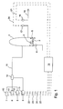
- an oven 1 is provided with a door 2 which might be opened to place a substrate 3 in the interior of oven 1.
- the outside seal of door 2 is flushed with nitrogen gas provided by a nitrogen valve 4. Small amounts of nitrogen gas are leaking into the interior of oven 1 through leaks 5 between the oven and the edge of door 2.
- Oven 1 is provided with a flange 26 which has an opening 27. Opening 27 is connected to nitrogen valve 4.
- the surface of door 2 fits closely to the surface of flange 26.
- Door 2 is provided with a groove 28, which is extending parallel to the edge of door 2. Nitrogen coming from nitrogen valve 4 is entering groove 28 through opening 27, is then flowing through groove 28 and then leaves groove 28 through a further opening (not shown). Between the surfaces of flange 26 and door 2 a small leak 5 forms. Through leak 5 either reaction gases may flow from the interior of oven 1 towards groove 28 or nitrogen gas may flow from groove 28 towards the interior of oven 1. Groove 28 may also be provided at the oven flange 26 as shown in fig. 2a. The reaction gases entering groove 28 are flushed away by the nitrogen gas flowing in groove 28.
- a torch 14 To prepare an oxidising medium four feeds are provided in the device shown in fig. 1, feeding oxygen 6, nitrogen 7, hydrogen chloride 8 and hydrogen 9 to a torch 14.
- the feed of the gases can be controlled by mass flow controllers 10 - 13, respectively.
- water vapour is produced by an oxyhydrogen flame.
- the oxidising medium consisting of nitrogen, hydrogen chloride, water vapour and excess oxygen is then fed to oven 1 by a pipe 15.
- the surface of substrate 3 is oxidised by the oxidation medium.
- the exhaust gases are then removed from the interior of oven 1 by an exhaust 16.
- a sensor 17 In the exhaust is provided a sensor 17 for determining the total pressure inside the oven and a sensor 18 for determining the oxygen concentration in the exhaust gases.
- Signals corresponding to the total pressure determined by sensor 17 and the oxygen concentration determined by sensor 18 are provided to a computer by wires 20 and 21, respectively.
- computer 19 the partial oxygen pressure in the exhaust gases is calculated based on the information provided by sensors 17 and 18.
- the calculated partial pressure of oxygen is then compared to a set point defined for the oxygen partial pressure and a deviation from the set point is calculated.
- new set points are calculated for the oxygen, nitrogen, hydrogen chloride and hydrogen feeds 6 - 9, respectively.
- a signal is then sent to mass flow controllers 10 - 13 by wires 22 - 25 to adjust the feed of the oxygen medium components to the new set points.
Landscapes
- Chemical & Material Sciences (AREA)
- Engineering & Computer Science (AREA)
- Materials Engineering (AREA)
- Metallurgy (AREA)
- Organic Chemistry (AREA)
- Crystallography & Structural Chemistry (AREA)
- Chemical Kinetics & Catalysis (AREA)
- Mechanical Engineering (AREA)
- Formation Of Insulating Films (AREA)
Priority Applications (4)
| Application Number | Priority Date | Filing Date | Title |
|---|---|---|---|
| EP01115213A EP1271636A1 (en) | 2001-06-22 | 2001-06-22 | Thermal oxidation process control by controlling oxidation agent partial pressure |
| PCT/EP2002/006908 WO2003001580A1 (en) | 2001-06-22 | 2002-06-21 | Thermal oxidation process control by controlling oxidation agent partial pressure |
| JP2003507877A JP3895326B2 (ja) | 2001-06-22 | 2002-06-21 | 酸化剤の分圧の制御による熱酸化プロセス制御 |
| US10/481,426 US20040219800A1 (en) | 2001-06-22 | 2002-06-21 | Thermal oxidation process control by controlling oxidation agent partial pressure |
Applications Claiming Priority (1)
| Application Number | Priority Date | Filing Date | Title |
|---|---|---|---|
| EP01115213A EP1271636A1 (en) | 2001-06-22 | 2001-06-22 | Thermal oxidation process control by controlling oxidation agent partial pressure |
Publications (1)
| Publication Number | Publication Date |
|---|---|
| EP1271636A1 true EP1271636A1 (en) | 2003-01-02 |
Family
ID=8177797
Family Applications (1)
| Application Number | Title | Priority Date | Filing Date |
|---|---|---|---|
| EP01115213A Withdrawn EP1271636A1 (en) | 2001-06-22 | 2001-06-22 | Thermal oxidation process control by controlling oxidation agent partial pressure |
Country Status (4)
| Country | Link |
|---|---|
| US (1) | US20040219800A1 (https=) |
| EP (1) | EP1271636A1 (https=) |
| JP (1) | JP3895326B2 (https=) |
| WO (1) | WO2003001580A1 (https=) |
Cited By (1)
| Publication number | Priority date | Publication date | Assignee | Title |
|---|---|---|---|---|
| WO2008133752A3 (en) * | 2006-12-18 | 2010-12-16 | President And Fellows Of Harvard College | Nanoscale oxide coatings |
Families Citing this family (27)
| Publication number | Priority date | Publication date | Assignee | Title |
|---|---|---|---|---|
| US7727904B2 (en) * | 2005-09-16 | 2010-06-01 | Cree, Inc. | Methods of forming SiC MOSFETs with high inversion layer mobility |
| JP5792972B2 (ja) * | 2011-03-22 | 2015-10-14 | 株式会社日立国際電気 | 半導体装置の製造方法及び基板処理装置 |
| US9984894B2 (en) | 2011-08-03 | 2018-05-29 | Cree, Inc. | Forming SiC MOSFETs with high channel mobility by treating the oxide interface with cesium ions |
| US10224224B2 (en) | 2017-03-10 | 2019-03-05 | Micromaterials, LLC | High pressure wafer processing systems and related methods |
| US10622214B2 (en) | 2017-05-25 | 2020-04-14 | Applied Materials, Inc. | Tungsten defluorination by high pressure treatment |
| US10847360B2 (en) | 2017-05-25 | 2020-11-24 | Applied Materials, Inc. | High pressure treatment of silicon nitride film |
| KR102574914B1 (ko) | 2017-06-02 | 2023-09-04 | 어플라이드 머티어리얼스, 인코포레이티드 | 보론 카바이드 하드마스크의 건식 스트리핑 |
| US10276411B2 (en) | 2017-08-18 | 2019-04-30 | Applied Materials, Inc. | High pressure and high temperature anneal chamber |
| JP6947914B2 (ja) | 2017-08-18 | 2021-10-13 | アプライド マテリアルズ インコーポレイテッドApplied Materials,Incorporated | 高圧高温下のアニールチャンバ |
| CN111095524B (zh) | 2017-09-12 | 2023-10-03 | 应用材料公司 | 用于使用保护阻挡物层制造半导体结构的设备和方法 |
| US10643867B2 (en) | 2017-11-03 | 2020-05-05 | Applied Materials, Inc. | Annealing system and method |
| KR102585074B1 (ko) | 2017-11-11 | 2023-10-04 | 마이크로머티어리얼즈 엘엘씨 | 고압 프로세싱 챔버를 위한 가스 전달 시스템 |
| SG11202003438QA (en) | 2017-11-16 | 2020-05-28 | Applied Materials Inc | High pressure steam anneal processing apparatus |
| JP2021503714A (ja) | 2017-11-17 | 2021-02-12 | アプライド マテリアルズ インコーポレイテッドApplied Materials,Incorporated | 高圧処理システムのためのコンデンサシステム |
| TWI794363B (zh) * | 2017-12-20 | 2023-03-01 | 美商應用材料股份有限公司 | 金屬薄膜之高壓氧化 |
| JP7299898B2 (ja) | 2018-01-24 | 2023-06-28 | アプライド マテリアルズ インコーポレイテッド | 高圧アニールを用いたシーム修復 |
| CN111902929B (zh) | 2018-03-09 | 2025-09-19 | 应用材料公司 | 用于含金属材料的高压退火处理 |
| US10714331B2 (en) | 2018-04-04 | 2020-07-14 | Applied Materials, Inc. | Method to fabricate thermally stable low K-FinFET spacer |
| US10950429B2 (en) | 2018-05-08 | 2021-03-16 | Applied Materials, Inc. | Methods of forming amorphous carbon hard mask layers and hard mask layers formed therefrom |
| US10566188B2 (en) | 2018-05-17 | 2020-02-18 | Applied Materials, Inc. | Method to improve film stability |
| US10704141B2 (en) | 2018-06-01 | 2020-07-07 | Applied Materials, Inc. | In-situ CVD and ALD coating of chamber to control metal contamination |
| US10748783B2 (en) | 2018-07-25 | 2020-08-18 | Applied Materials, Inc. | Gas delivery module |
| US10675581B2 (en) | 2018-08-06 | 2020-06-09 | Applied Materials, Inc. | Gas abatement apparatus |
| JP7179172B6 (ja) | 2018-10-30 | 2022-12-16 | アプライド マテリアルズ インコーポレイテッド | 半導体用途の構造体をエッチングするための方法 |
| KR20210077779A (ko) | 2018-11-16 | 2021-06-25 | 어플라이드 머티어리얼스, 인코포레이티드 | 강화된 확산 프로세스를 사용한 막 증착 |
| WO2020117462A1 (en) | 2018-12-07 | 2020-06-11 | Applied Materials, Inc. | Semiconductor processing system |
| US11901222B2 (en) | 2020-02-17 | 2024-02-13 | Applied Materials, Inc. | Multi-step process for flowable gap-fill film |
Citations (4)
| Publication number | Priority date | Publication date | Assignee | Title |
|---|---|---|---|---|
| JPS6060730A (ja) * | 1983-09-14 | 1985-04-08 | Hitachi Ltd | 半導体装置の製造法 |
| JPH06283712A (ja) * | 1993-03-26 | 1994-10-07 | Ricoh Co Ltd | Mos型半導体装置におけるゲート酸化膜の製造方法 |
| JPH0774166A (ja) * | 1993-09-02 | 1995-03-17 | Seiko Epson Corp | 熱処理装置 |
| EP0957184A2 (en) * | 1998-04-16 | 1999-11-17 | The Boc Group, Inc. | Sputtering control system |
Family Cites Families (3)
| Publication number | Priority date | Publication date | Assignee | Title |
|---|---|---|---|---|
| JPH08172084A (ja) * | 1994-12-19 | 1996-07-02 | Kokusai Electric Co Ltd | 半導体成膜方法及びその装置 |
| US6372663B1 (en) * | 2000-01-13 | 2002-04-16 | Taiwan Semiconductor Manufacturing Company, Ltd | Dual-stage wet oxidation process utilizing varying H2/O2 ratios |
| JP2001274154A (ja) * | 2000-01-18 | 2001-10-05 | Applied Materials Inc | 成膜方法、成膜装置、半導体装置及びその製造方法 |
-
2001
- 2001-06-22 EP EP01115213A patent/EP1271636A1/en not_active Withdrawn
-
2002
- 2002-06-21 US US10/481,426 patent/US20040219800A1/en not_active Abandoned
- 2002-06-21 JP JP2003507877A patent/JP3895326B2/ja not_active Expired - Fee Related
- 2002-06-21 WO PCT/EP2002/006908 patent/WO2003001580A1/en not_active Ceased
Patent Citations (4)
| Publication number | Priority date | Publication date | Assignee | Title |
|---|---|---|---|---|
| JPS6060730A (ja) * | 1983-09-14 | 1985-04-08 | Hitachi Ltd | 半導体装置の製造法 |
| JPH06283712A (ja) * | 1993-03-26 | 1994-10-07 | Ricoh Co Ltd | Mos型半導体装置におけるゲート酸化膜の製造方法 |
| JPH0774166A (ja) * | 1993-09-02 | 1995-03-17 | Seiko Epson Corp | 熱処理装置 |
| EP0957184A2 (en) * | 1998-04-16 | 1999-11-17 | The Boc Group, Inc. | Sputtering control system |
Non-Patent Citations (5)
| Title |
|---|
| "PRECISION INSTRUMENTS LEAVE LAB, ENTER PROCESS AREAS", MACHINE DESIGN, PENTON,INC. CLEVELAND, US, vol. 61, no. 4, 23 February 1989 (1989-02-23), pages 66, XP000052320, ISSN: 0024-9114 * |
| AHMED W ET AL: "A COMPARATIVE INVESTIGATION OF THE OXIDATION OF SILICON USING H2/O2, TCA/O2 AND HCI/O2 MIXTURES", ADVANCED MATERIALS FOR OPTICS AND ELECTRONICS, WILEY AND SONS LTD, CHICHESTER, GB, vol. 2, no. 4, 1 July 1993 (1993-07-01), pages 165 - 173, XP000384607, ISSN: 1057-9257 * |
| PATENT ABSTRACTS OF JAPAN vol. 009, no. 193 (E - 334) 9 August 1985 (1985-08-09) * |
| PATENT ABSTRACTS OF JAPAN vol. 1995, no. 01 28 February 1995 (1995-02-28) * |
| PATENT ABSTRACTS OF JAPAN vol. 1995, no. 06 31 July 1995 (1995-07-31) * |
Cited By (1)
| Publication number | Priority date | Publication date | Assignee | Title |
|---|---|---|---|---|
| WO2008133752A3 (en) * | 2006-12-18 | 2010-12-16 | President And Fellows Of Harvard College | Nanoscale oxide coatings |
Also Published As
| Publication number | Publication date |
|---|---|
| WO2003001580A1 (en) | 2003-01-03 |
| JP3895326B2 (ja) | 2007-03-22 |
| JP2004531079A (ja) | 2004-10-07 |
| US20040219800A1 (en) | 2004-11-04 |
Similar Documents
| Publication | Publication Date | Title |
|---|---|---|
| EP1271636A1 (en) | Thermal oxidation process control by controlling oxidation agent partial pressure | |
| TWI400756B (zh) | 基板處理裝置、基板處理方法及半導體裝置之製造方法 | |
| US7953512B2 (en) | Substrate processing system, control method for substrate processing apparatus and program stored on medium | |
| US5118286A (en) | Closed loop method and apparatus for preventing exhausted reactant gas from mixing with ambient air and enhancing repeatability of reaction gas results on wafers | |
| US6171104B1 (en) | Oxidation treatment method and apparatus | |
| JPWO2007111351A1 (ja) | 半導体装置の製造方法 | |
| US20040007186A1 (en) | Heat-treating device | |
| JP2004531079A5 (https=) | ||
| CN1218370C (zh) | 热处理装置 | |
| JP7838899B2 (ja) | 基板処理方法及び基板処理装置 | |
| KR100277142B1 (ko) | 오존유량제어장치 | |
| JP2012054393A (ja) | 基板処理装置及び半導体装置の製造方法 | |
| US20050064609A1 (en) | Semiconductor processing system | |
| JP2020184552A (ja) | 成膜方法及び成膜装置 | |
| US7004012B2 (en) | Method of estimating thickness of oxide layer | |
| EP1357582A1 (en) | Heat-treating device | |
| JP7680122B2 (ja) | 異常検出方法及び処理装置 | |
| CN114341399B (zh) | 基板处理装置、基板处理方法、半导体装置的制造方法以及计算机可读记录介质 | |
| JP2002286574A5 (https=) | ||
| KR100808372B1 (ko) | 화학기상증착장치의 진공 시스템 및 이의 제어 방법 | |
| JPH10330943A (ja) | 薄膜気相成長装置 | |
| JPH11204511A (ja) | シリコン熱酸化膜の形成装置 | |
| JPS6082668A (ja) | ガス流量制御装置 | |
| US6594182B1 (en) | Semiconductor memory device having controlled impurity concentration profile, method for manufacturing thereof, and semiconductor manufacturing apparatus | |
| KR20140037583A (ko) | 오존 발생기를 구비하는 반도체 소자의 제조 장치 |
Legal Events
| Date | Code | Title | Description |
|---|---|---|---|
| PUAI | Public reference made under article 153(3) epc to a published international application that has entered the european phase |
Free format text: ORIGINAL CODE: 0009012 |
|
| AK | Designated contracting states |
Kind code of ref document: A1 Designated state(s): AT BE CH CY DE DK ES FI FR GB GR IE IT LI LU MC NL PT SE TR |
|
| AX | Request for extension of the european patent |
Free format text: AL;LT;LV;MK;RO;SI |
|
| 17P | Request for examination filed |
Effective date: 20030616 |
|
| AKX | Designation fees paid |
Designated state(s): DE FR GB IE IT NL |
|
| 17Q | First examination report despatched |
Effective date: 20060703 |
|
| 17Q | First examination report despatched |
Effective date: 20060703 |
|
| STAA | Information on the status of an ep patent application or granted ep patent |
Free format text: STATUS: THE APPLICATION IS DEEMED TO BE WITHDRAWN |
|
| 18D | Application deemed to be withdrawn |
Effective date: 20090102 |