EP1253498A1 - Spannungsregler - Google Patents
Spannungsregler Download PDFInfo
- Publication number
- EP1253498A1 EP1253498A1 EP02008935A EP02008935A EP1253498A1 EP 1253498 A1 EP1253498 A1 EP 1253498A1 EP 02008935 A EP02008935 A EP 02008935A EP 02008935 A EP02008935 A EP 02008935A EP 1253498 A1 EP1253498 A1 EP 1253498A1
- Authority
- EP
- European Patent Office
- Prior art keywords
- transistor
- current
- voltage regulator
- flowing
- regulator according
- Prior art date
- Legal status (The legal status is an assumption and is not a legal conclusion. Google has not performed a legal analysis and makes no representation as to the accuracy of the status listed.)
- Granted
Links
- 230000000087 stabilizing effect Effects 0.000 claims abstract description 9
- 230000001419 dependent effect Effects 0.000 claims abstract description 5
- 101100462365 Aspergillus niger (strain CBS 513.88 / FGSC A1513) otaA gene Proteins 0.000 description 34
- 230000006641 stabilisation Effects 0.000 description 21
- 238000011105 stabilization Methods 0.000 description 21
- 239000003990 capacitor Substances 0.000 description 9
- 101100462367 Aspergillus niger (strain CBS 513.88 / FGSC A1513) otaB gene Proteins 0.000 description 8
- 238000012546 transfer Methods 0.000 description 6
- 230000007423 decrease Effects 0.000 description 3
- 238000013461 design Methods 0.000 description 3
- 238000010586 diagram Methods 0.000 description 2
- 230000005611 electricity Effects 0.000 description 2
- 238000000034 method Methods 0.000 description 2
- 230000003321 amplification Effects 0.000 description 1
- 238000013459 approach Methods 0.000 description 1
- 238000011161 development Methods 0.000 description 1
- 230000018109 developmental process Effects 0.000 description 1
- 230000001939 inductive effect Effects 0.000 description 1
- 238000003199 nucleic acid amplification method Methods 0.000 description 1
- 230000003071 parasitic effect Effects 0.000 description 1
- 230000008092 positive effect Effects 0.000 description 1
Images


Classifications
-
- G—PHYSICS
- G05—CONTROLLING; REGULATING
- G05F—SYSTEMS FOR REGULATING ELECTRIC OR MAGNETIC VARIABLES
- G05F1/00—Automatic systems in which deviations of an electric quantity from one or more predetermined values are detected at the output of the system and fed back to a device within the system to restore the detected quantity to its predetermined value or values, i.e. retroactive systems
- G05F1/10—Regulating voltage or current
- G05F1/46—Regulating voltage or current wherein the variable actually regulated by the final control device is DC
- G05F1/56—Regulating voltage or current wherein the variable actually regulated by the final control device is DC using semiconductor devices in series with the load as final control devices
- G05F1/575—Regulating voltage or current wherein the variable actually regulated by the final control device is DC using semiconductor devices in series with the load as final control devices characterised by the feedback circuit
-
- G—PHYSICS
- G05—CONTROLLING; REGULATING
- G05F—SYSTEMS FOR REGULATING ELECTRIC OR MAGNETIC VARIABLES
- G05F3/00—Non-retroactive systems for regulating electric variables by using an uncontrolled element, or an uncontrolled combination of elements, such element or such combination having self-regulating properties
- G05F3/02—Regulating voltage or current
- G05F3/08—Regulating voltage or current wherein the variable is DC
- G05F3/10—Regulating voltage or current wherein the variable is DC using uncontrolled devices with non-linear characteristics
- G05F3/16—Regulating voltage or current wherein the variable is DC using uncontrolled devices with non-linear characteristics being semiconductor devices
- G05F3/20—Regulating voltage or current wherein the variable is DC using uncontrolled devices with non-linear characteristics being semiconductor devices using diode- transistor combinations
- G05F3/26—Current mirrors
- G05F3/262—Current mirrors using field-effect transistors only
Definitions
- the present invention relates to a device according to the Preamble of claim 1, i.e. a voltage regulator, whose output voltage from the control of a Voltage regulator contained transistor depends.
- the voltage regulator generates an output voltage Vout, which is tapped at the source of the transistor MN1, and which of the load Zout supplied as a supply voltage becomes.
- the drain of transistor MN1 is connected to a the voltage regulator with energy supply voltage applied, and the gate terminal is with the output terminal of the transconductance amplifier OTA1.
- the transconductance amplifier OTA1 has two input connections from which an input voltage Vin is supplied, and of which the other one of the output voltage Vout dependent (fed back) voltage supplied becomes; the transconductance amplifier OTA1 forms the Difference between these voltages and indicates the result the gate terminal of transistor MN1.
- the feedback Voltage is applied to one between the resistors Rfb and Re tapped node x2; the resistors Rfb and Re are connected in series and between the source connection of transistor MN1 and ground.
- the voltage regulator described is a series regulator (Series Voltage Regulator) with an NMOS transistor in basic drain circuit as a driver stage. It should be obvious and needed no further explanation that the voltage regulator shown is able to create one of Vin and the (through the Resistances Rfb and Re determined) depending on feedback factor to generate constant output voltage Vout. This is however, especially with complex loads Zout, i.e. at No loads with inductive and / or capacitive components guaranteed under all circumstances: the system can in this Case become unstable.
- the stabilization circuit can ensure that the through current flowing in phases in the transistor, and only in Phases in which this would be too small to be stable To ensure operation of the voltage regulator is increased.
- the voltage regulator according to the invention has a lower energy requirement, because the flow of the additional cross flow will yes only initiated in certain phases.
- FIG. 1 An arrangement is shown in FIG stabilized voltage regulator and a connected to it Load impedance Zout includes.
- the voltage regulator is a series voltage regulator that like that shown in Figure 5 and initially with reference voltage regulator described there a differential amplifier (a differential transconductance amplifier) OTA1, one NMOS transistor MN1, a first resistor Rfb and one contains second resistance Re, which is also the case in the Figure 5 shown voltage regulator are connected and cooperate.
- the voltage regulator shown in Figure 1 contains in addition a stabilization circuit, which however is constructed and works completely differently than that for stabilization serving elements Rs, Cs1, Cs2 and Cs3 of the voltage regulator according to FIG. 5.
- From transistor MP3 is the source connection with the node x3 connected, the gate terminal is connected to the output terminal of the second transconductance amplifier OTA2, and is the drain connection with the source connection of the transistor MN4 connected.
- the drain connection of the (also grounded on the source side) Transistor MN3 is connected to a node x1. With this node x1 there is also a current Iref output reference current source and the drain connection of the transistor MN5 connected.
- the transistor MN5 (grounded on the source side) is included the transistor MN6 connected to a current mirror, wherein a current Ic flowing through transistor MN5 causes a current Ic 'flows through the transistor MN6.
- the transconductance amplifier OTA2 and the transistor MP3 ensure that the source of the transistor MN2 (at node x3) sets the same potential as on Source connection of the transistor MN1. I.e. that on Node x3 sets the potential Vout. Simplified lets the arrangement of transconductance amplifier OTA2 and Understand transistor MP3 as a voltage follower of a replica the output voltage Vout at node x3.
- the transistors MN1 and MN2 are thus in the voltage same working point, which is the improvement of synchronism serves both transistors to each other.
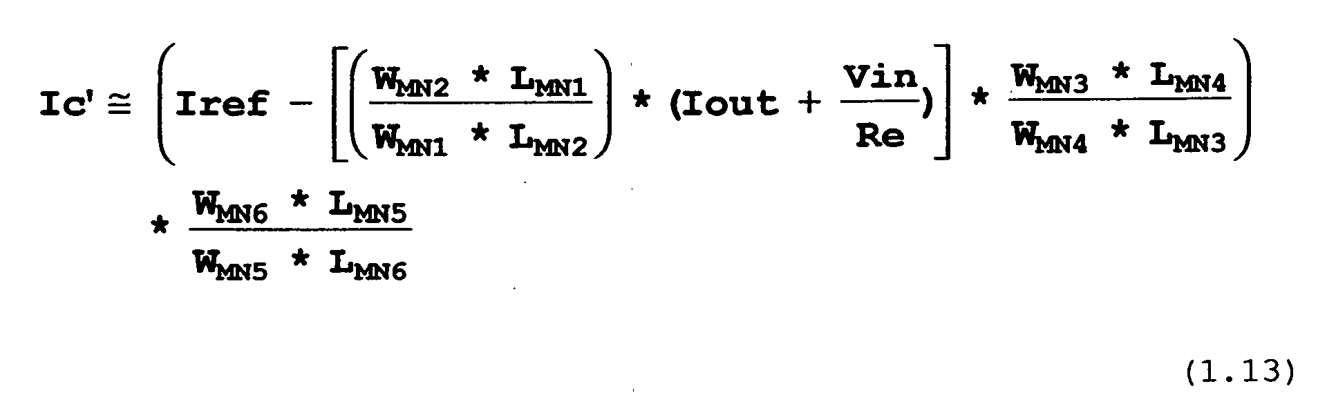
- the transistor MN2 by the same signal how the transistor MN1 is driven on the gate side A current flowing through transistor MN2, which is in a determined ratio to the flowing through the transistor MN1 Electricity is there.
- the transistor is preferably very much weaker than the transistor MN1, so that the Transistor MN2 current flowing through Irep is much smaller is than the current Ic '+ Iq flowing through the transistor MN1 + Lout.
- the transistor MN2 thus provides a replica current Irep current Ic '+ Iq + Iout flowing through to the transistor MN1.
- the stabilization circuit can thus achieve that the transistor MN1 from an additional cross current Ic ' is flowed through when the sum of the currents Iout and Iq is small, and that transistor MN1 has no additional Cross current Ic 'is flowed through when the sum of the currents Iout and Iq is big, big enough to be one to ensure stable operation of the voltage regulator.
- the voltage regulator according to FIG. 1 also contains Capacitors Cm1 and Cm2, through which the output connections the transconductance amplifier OTA1 and OTA2 connected to ground are, and which for frequency compensation of the transconductance amplifier OTA1 and OTA2 serve.
- Vout Vout ⁇ Vin * Rfb + Re re
- the current Is1 is minimal when Iout and Ic 'are equal to and equal to 0
- the current Is1 in the transistor MN1 decreases and thus also the current in the transistor MN2.
- the circuit can now be dimensioned accordingly using equations 1.29, 1.14 and 1.15.
- a structure and a value must be defined at the beginning of the dimensioning. This can be done from a specification for the bandwidth of the OTA according to equation 1.16.
- the minimum current Iq flows as Is1. The circuit thus has a corresponding reserve in terms of stability.
- Equations 1.35 and 1.29 can now be used for those in the figures 1 and 2 arrangements shown the minimum cross current be determined by the output transistor MN1 or MP1 must flow to at a given load capacity to ensure stability.
- the resistance Rmin (Rmin ') as an auxiliary variable serves for dimensioning.
- the stream accepted by one Resistance Rmin (Rmin ') can now be between the Current Iq through voltage dividers Rfb and Re and the current Ic ' be divided. The circuit can thus be fully dimensioned.
- the transfer function shows an increase in the frequency range to the expected DC gain, this is from an instability or to assume at least one ringing.
- the circuit can be made accordingly be dimensioned.
- a stabilization circuit is shown in FIG which for turning on and turning off the additional Cross current Ic 'a hysteresis is provided.
- FIG. 4 largely corresponds the arrangement shown in Figure 1; with the same Elements identified by reference numerals are identical or corresponding elements.
- the stabilization circuit shown in FIG. 4 contains additionally NMOS transistors MN7 and MN8 and one Current source supplying reference current Iref2.
- the transistors MN7 and MN8 are connected to form a current mirror, the drain of transistor MN7 and the Gate connections of transistors MN7 and MN8 with node x1 are connected, the drain of the transistor MN8 to the Drain connection of the transistor MN4, the gate connections of the Transistors MN3 and MN4 and the reference current Iref2 supplying power source is connected, and the source connections of transistors MN7 and MN8 connected to ground are.
- the additional measures ensure that the Threshold that Irep must fall below so that the additional cross current Ic 'flows is smaller than that Threshold that must be exceeded by Irep so that no additional cross current Ic 'flows.
- the change of the current flowing through the transistor MN1 or MP1 done by reconfiguring the arrangement, for example by opening, closing or switching switches, via which the transistor acts as load elements Components or current sinks can be connected.
- the stabilizing circuits of the voltage regulators described are independent of the details of practical Realization easy to design and implement, and can with minimal own energy requirement of the voltage regulator one under ensure reliable stabilization in all circumstances.
Landscapes
- Engineering & Computer Science (AREA)
- Physics & Mathematics (AREA)
- Electromagnetism (AREA)
- General Physics & Mathematics (AREA)
- Radar, Positioning & Navigation (AREA)
- Automation & Control Theory (AREA)
- Continuous-Control Power Sources That Use Transistors (AREA)
- Amplifiers (AREA)
Abstract
Description
- der Widerstand Rs und der Kondensator Cs1 in Reihe geschaltet und zwischen dem Ausgangsanschluß des Transkonduktanzverstärkers OTA1 und Masse angeordnet,
- der Kondensator Cs2 zwischen dem Rückkoppelzweig und Masse angeordnet, und
- der Kondensator Cs3 parallel zum Widerstand Rfb angeordnet. Durch die genannten Elemente kann Einfluß auf die Lage der Pol- und Nullstellen der Übertragungsfunktion und damit auch auf das Stabilitätsverhalten des Systems genommen werden. Allerdings ist es schwierig und aufwendig, und teilweise sogar unmöglich, die genannten Elemente so zu dimensionieren, daß der Spannungsregler über den gesamten Lastbereich stabil arbeitet. Es existiert eine Vielzahl von Veröffentlichungen, in welchen diese und weitere Möglichkeiten zur Stabilisierung von Spannungsreglern beschrieben sind. Es wird beispielsweise auf
- Thomas M. Frederiksen: "A Monolithic High-Power Series Voltage Regulator", IEEE Journal of Solid-State Circuits, Dezember 1968, Seite 380 ff.,
- Gabriel A. Rincon-Mora et al.: "A Low-Voltage, Low Quiescent Current, Low Drop-Out Regulator", IEEE Journal of Solid-State Circuits, Vol.33, No. 1., January 1998, Seiten 36 ff., und
- Gerrit W. den Besten et al.: "Embedded 5V-to-3.3V Voltage
Regulator for Supplying Digital IC's in 3.3V CMOS Technology",
IEEE Journal of Solid-State Circuits, Vol 33, No.
7, July 1998, Seite 956 ff.
und die darin genannten weiteren Fundstellen verwiesen.
- Figur 1
- einen Series Voltage Regulator mit einer im folgenden näher beschriebenen Stabilisierungsschaltung,
- Figur 2
- einen Low Drop Output Regulator mit der im folgenden näher beschriebenen Stabilisierungsschaltung,
- Figur 3
- die zeitlichen Verläufe ausgewählter Ströme und Spannungen in der in der Figur 1 gezeigten Anordnung,
- Figur 4
- einen Series Voltage Regulator mit einer modifizierten Stabilisierungsschaltung,
- Figur 5
- einen herkömmlichen Series-Voltage Regulator, und
- Figur 6
- ein vereinfachtes Kleinsignal-Ersatzschaltbild der in der Figur 5 gezeigten Anordnung.
- daß anstelle des NMOS-Treibertransistors MN1 in Drain-Grundschaltung ein PMOS-Treibertransistor MP1 in Source-Grundschaltung verwendet wird, und
- daß die Frequenzkompensation des ersten Transkonduktanzverstärkers OTA1 durch eine zwischen dem Ausgangsanschluß des Transkonduktanzverstärkers OTA1 und dem Ausgangsanschluß des Spannungsreglers (dem Drainanschluß des Transistors MP1) angeordnete Reihenschaltung eines Kondensators Cm1 und eines Widerstandes Rm1 erfolgt (Stichwort: Millerkompensation bzw. Polsplitting).




- R1 den Ausgangswiderstand des Transkonduktanzverstärkers OTA1,
- gdsp den Ausgangsleitwert eines P-Kanal MOS-Transistors,
- gdsn den Ausgangsleitwert eines N-Kanal MOS-Transistors,
- C1 die Summe der Lastkapazitäten am Knoten X4 (Ausgang OTA1),
- CgsMP1 die Gate-Source-Kapazität des Transistors MP1,
- CgdMP1 die Gate-Drain-Kapazität des Transistors MP1,
- Av11 die Gleichspannungsverstärkung der Ausgangsstufe (z.B. Transistor MP1),
- R2 den Ausgangswiderstand der Treiberanordnung,
- gdsMP1 den Ausgangsleitwert des Transistors MP1,
- Rout den rein resistiven Lastwiderstand am Knoten Vout,
- Rmin die minimalste Summenresitivität aus Rfb und Re als Hilfsgröße zur Dimensionierung,
- C2 die transformierte Lastkapazität zur Berechnung des zweiten Pols fp2', und
- gmMP1 die Steilheit des Ausgangstransistors MP1 bezeichnen.



- Cx
- Kondensatoren
- Ix
- Ströme
- MNx
- NMOS-Transustoren
- MPx
- PMOS-Transistoren
- OTAx
- Transkonduktanzverstärker
- Rx
- Widerstände
- Vx
- Spannungen
- Zout
- Lastwiderstand
Claims (15)
- Spannungsregler, dessen Ausgangsspannung (Vout) von der Ansteuerung eines im Spannungsregler enthaltenen Transistors (MN1, MP1) abhängt,
dadurch gekennzeichnet, daß der Spannungsregler eine Stabilisierungsschaltung enthält, welche den durch den Transistor (MN1, MP1) fließenden Strom (Is1) verändern kann. - Spannungsregler nach Anspruch 1,
dadurch gekennzeichnet, daß die Veränderung des durch den Transistor (MN1, MP1) fließenden Stromes (Is1) dadurch erfolgt, daß die vom Transistor getriebene Last verändert wird. - Spannungsregler nach Anspruch 2,
dadurch gekennzeichnet, daß die Veränderung der vom Transistor (MN1, MP1) getriebenen Last durch eine Umkonfigurierung des Spannungsreglers erfolgt. - Spannungsregler nach Anspruch 3,
dadurch gekennzeichnet, daß die Umkonfigurierung durch Öffnen, Schließen oder eines Schalters erfolgt, über welche der Transistor (MN1, MP1) mit einem als Lastelement wirkenden Bauteil oder einer Stromsenke verbunden werden kann. - Spannungsregler nach Anspruch 1,
dadurch gekennzeichnet, daß die Veränderung des durch den Transistor (MN1, MP1) fließenden Stromes (Is1) durch eine Veränderung der Ansteuerung eines Bauelementes erfolgt, das in einem den Transistor enthaltenden Schaltungszweig angeordnet ist. - Spannungsregler nach Anspruch 5,
dadurch gekennzeichnet, daß die Veränderung des durch den Transistor (MN1, MP1) fließenden Stromes (Is1) dadurch erfolgt, daß die Ansteuerung eines zum Transistor in Reihe geschalteten zweiten Transistors (MN6) verändert wird. - Spannungsregler nach Anspruch 6,
dadurch gekennzeichnet, daß der zweite Transistor (MN6) mit einem dritten Transistor (MN5) zu einem Stromspiegel verschaltet ist, und daß der durch den zweiten Transistor fließende Strom von dem durch den dritten Transistor fließenden Strom abhängt. - Spannungsregler nach einem der vorhergehenden Ansprüche,
dadurch gekennzeichnet, daß die Stabilisierungsschaltung eine Veränderung des durch den ersten Transistor (MN1, MP1) fließenden Stromes (Is1) veranlaßt, wenn und so lange der den Transistor durchfließende Strom eine Größe aufweist, bei welcher kein stabiler Betrieb des Spannungsreglers gewährleistet werden kann. - Spannungsregler nach einem der vorhergehenden Ansprüche,
dadurch gekennzeichnet, daß die Stabilisierungsschaltung den durch den ersten Transistor (MN1, MP1) fließenden Strom (Is1) nicht verändert, wenn und so lange der den Transistor durchfließende Strom eine Größe aufweist, bei welcher ein stabiler Betrieb des Spannungsreglers gewährleistet ist. - Spannungsregler nach Anspruch 8 oder 9,
dadurch gekennzeichnet, daß die Stabilisierungsschaltung einen Strom (Irep) erzeugt, dessen Größe ein Maß für den den ersten Transistor (MN1, MP1) durchfließenden Strom ist, und den durch den ersten Transistor fließenden Strom verändert, wenn der generierte Strom (Irep) oder ein davon abhängender Strom (Irep') kleiner als ein Referenzstrom (Iref) ist. - Spannungsregler nach Anspruch 10,
dadurch gekennzeichnet, daß die Generierung des Stromes durch einen vierten Transistor (MN2, MP2) erfolgt, der wie der erste Transistor (MN1, MP1) angesteuert wird. - Spannungsregler nach Anspruch 11,
dadurch gekennzeichnet, daß der vierte Transistor (MN2, MP2) kleiner dimensioniert ist als der erste Transistor (MN1, MP1). - Spannungsregler nach einem der Ansprüche 11 oder 12,
dadurch gekennzeichnet, daß die Stabilisierungsschaltung dafür sorgt, daß der vierte Transistor (MN2, MP2) im selben Arbeitspunkt betrieben wird wie der erste Transistor (MN1, MP1). - Spannungsregler nach einem der Ansprüche 10 bis 13,
dadurch gekennzeichnet, daß in Reihe zum vierten Transistor (MN2, MP2) ein fünfter Transistor (MN4) geschaltet ist, wobei dieser fünfte Transistor mit einem sechsten Transistor (MN3) zu einem zweiten Stromspiegel verschaltet ist, wobei dem Sourceanschluß des sechsten Transistors der Referenzstrom (Iref) zugeführt wird, und wobei der Sourceanschluß des sechsten Transistors mit dem primären Transistor (MN5) des ersten Stromspiegels (MN5, MN6) verbunden ist. - Spannungsregler nach einem der vorhergehenden Ansprüche,
dadurch gekennzeichnet, daß die Veränderung des durch den Transistor (MN1, MP1) fließenden Stromes (Is1) über eine Hystereseschleife erfolgt.
Applications Claiming Priority (2)
| Application Number | Priority Date | Filing Date | Title |
|---|---|---|---|
| DE10119858A DE10119858A1 (de) | 2001-04-24 | 2001-04-24 | Spannungsregler |
| DE10119858 | 2001-04-24 |
Publications (2)
| Publication Number | Publication Date |
|---|---|
| EP1253498A1 true EP1253498A1 (de) | 2002-10-30 |
| EP1253498B1 EP1253498B1 (de) | 2006-10-04 |
Family
ID=7682407
Family Applications (1)
| Application Number | Title | Priority Date | Filing Date |
|---|---|---|---|
| EP02008935A Expired - Lifetime EP1253498B1 (de) | 2001-04-24 | 2002-04-22 | Spannungsregler |
Country Status (3)
| Country | Link |
|---|---|
| US (1) | US6700361B2 (de) |
| EP (1) | EP1253498B1 (de) |
| DE (2) | DE10119858A1 (de) |
Cited By (9)
| Publication number | Priority date | Publication date | Assignee | Title |
|---|---|---|---|---|
| EP1365302A1 (de) * | 2002-05-20 | 2003-11-26 | Texas Instruments Incorporated | Regulierungseinrichtung mit kleiner Verlustspannung |
| WO2017075156A1 (en) * | 2015-10-30 | 2017-05-04 | Qualcomm Incorporated | Dual loop regulator circuit |
| US9946283B1 (en) | 2016-10-18 | 2018-04-17 | Qualcomm Incorporated | Fast transient response low-dropout (LDO) regulator |
| US10411599B1 (en) | 2018-03-28 | 2019-09-10 | Qualcomm Incorporated | Boost and LDO hybrid converter with dual-loop control |
| US10444780B1 (en) | 2018-09-20 | 2019-10-15 | Qualcomm Incorporated | Regulation/bypass automation for LDO with multiple supply voltages |
| US10545523B1 (en) | 2018-10-25 | 2020-01-28 | Qualcomm Incorporated | Adaptive gate-biased field effect transistor for low-dropout regulator |
| US10591938B1 (en) | 2018-10-16 | 2020-03-17 | Qualcomm Incorporated | PMOS-output LDO with full spectrum PSR |
| US11372436B2 (en) | 2019-10-14 | 2022-06-28 | Qualcomm Incorporated | Simultaneous low quiescent current and high performance LDO using single input stage and multiple output stages |
| US12276993B2 (en) | 2020-07-24 | 2025-04-15 | Qualcomm Incorporated | Charge pump based low dropout regulator |
Families Citing this family (40)
| Publication number | Priority date | Publication date | Assignee | Title |
|---|---|---|---|---|
| US7026824B2 (en) * | 2003-10-31 | 2006-04-11 | Faraday Technology Corp. | Voltage reference generator with negative feedback |
| DE102004029966A1 (de) * | 2004-06-21 | 2006-01-12 | Infineon Technologies Ag | Verpolungsschutzschaltung mit niedrigem Spannungsabfall |
| TWI261406B (en) * | 2004-07-08 | 2006-09-01 | Analog Integrations Corp | Charge pump DC/DC converter with constant-frequency operation |
| US7205828B2 (en) * | 2004-08-02 | 2007-04-17 | Silicon Laboratories, Inc. | Voltage regulator having a compensated load conductance |
| KR100621104B1 (ko) | 2004-08-25 | 2006-09-19 | 삼성전자주식회사 | 전자장치 |
| DE102004062249B4 (de) * | 2004-12-23 | 2007-12-06 | Infineon Technologies Ag | Spannungsregler |
| FR2881537B1 (fr) * | 2005-01-28 | 2007-05-11 | Atmel Corp | Regulateur cmos standard a bas renvoi, psrr eleve, bas bruit avec nouvelle compensation dynamique |
| US8054055B2 (en) * | 2005-12-30 | 2011-11-08 | Stmicroelectronics Pvt. Ltd. | Fully integrated on-chip low dropout voltage regulator |
| US7589507B2 (en) * | 2005-12-30 | 2009-09-15 | St-Ericsson Sa | Low dropout regulator with stability compensation |
| FR2898701A1 (fr) * | 2006-03-15 | 2007-09-21 | St Microelectronics Sa | Generation d'une tension de reference |
| TW200919922A (en) * | 2007-10-16 | 2009-05-01 | Richtek Technology Corp | Linear charger and method for controlling charging current |
| FR2925167B1 (fr) * | 2007-12-17 | 2010-02-19 | St Microelectronics Sa | Dispositif de mesure de courant |
| FR2925166B1 (fr) * | 2007-12-17 | 2010-05-21 | St Microelectronics Sa | Procede et dispositif de mesure de courant pour un convertisseur dc/dc |
| US8278893B2 (en) * | 2008-07-16 | 2012-10-02 | Infineon Technologies Ag | System including an offset voltage adjusted to compensate for variations in a transistor |
| US8232781B2 (en) * | 2008-12-23 | 2012-07-31 | Stmicroelectronics S.R.L. | Device for measuring the current flowing through a power transistor of a voltage regulator |
| US8378652B2 (en) * | 2008-12-23 | 2013-02-19 | Texas Instruments Incorporated | Load transient response time of LDOs with NMOS outputs with a voltage controlled current source |
| JP5361614B2 (ja) * | 2009-08-28 | 2013-12-04 | ルネサスエレクトロニクス株式会社 | 降圧回路 |
| US9112422B1 (en) | 2010-03-09 | 2015-08-18 | Vlt, Inc. | Fault tolerant power converter |
| US8610415B2 (en) * | 2011-03-07 | 2013-12-17 | Fairchild Semiconductor Corporation | Lambda correction for current foldback |
| US8674672B1 (en) * | 2011-12-30 | 2014-03-18 | Cypress Semiconductor Corporation | Replica node feedback circuit for regulated power supply |
| RU2592719C2 (ru) * | 2012-03-16 | 2016-07-27 | Интел Корпорейшн | Генератор опорного напряжения с низким импедансом |
| US8742819B2 (en) * | 2012-09-25 | 2014-06-03 | Texas Instruments Incorporated | Current limiting circuitry and method for pass elements and output stages |
| US9122292B2 (en) * | 2012-12-07 | 2015-09-01 | Sandisk Technologies Inc. | LDO/HDO architecture using supplementary current source to improve effective system bandwidth |
| FR3000576B1 (fr) * | 2012-12-27 | 2016-05-06 | Dolphin Integration Sa | Circuit d'alimentation |
| US8917070B2 (en) * | 2013-03-14 | 2014-12-23 | Vidatronic, Inc. | LDO and load switch supporting a wide range of load capacitance |
| US20140266106A1 (en) * | 2013-03-14 | 2014-09-18 | Vidatronic, Inc. | Ldo and load switch supporting a wide range of load capacitance |
| US9170593B2 (en) * | 2013-05-16 | 2015-10-27 | Fairchild Semiconductor Corporation | Voltage regulator with improved line rejection |
| US9793707B2 (en) * | 2013-05-28 | 2017-10-17 | Texas Instruments Incorporated | Fast transient precision power regulation apparatus |
| US10185339B2 (en) * | 2013-09-18 | 2019-01-22 | Texas Instruments Incorporated | Feedforward cancellation of power supply noise in a voltage regulator |
| US9535439B2 (en) * | 2013-11-08 | 2017-01-03 | Texas Instruments Incorporated | LDO current limit control with sense and control transistors |
| US9436196B2 (en) * | 2014-08-20 | 2016-09-06 | Taiwan Semiconductor Manufacturing Company, Ltd. | Voltage regulator and method |
| DE102015216493B4 (de) * | 2015-08-28 | 2021-07-08 | Dialog Semiconductor (Uk) Limited | Linearer Regler mit verbesserter Stabilität |
| US10158357B1 (en) | 2016-04-05 | 2018-12-18 | Vlt, Inc. | Method and apparatus for delivering power to semiconductors |
| US10785871B1 (en) | 2018-12-12 | 2020-09-22 | Vlt, Inc. | Panel molded electronic assemblies with integral terminals |
| US10277105B1 (en) | 2016-04-05 | 2019-04-30 | Vlt, Inc. | Method and apparatus for delivering power to semiconductors |
| US11336167B1 (en) | 2016-04-05 | 2022-05-17 | Vicor Corporation | Delivering power to semiconductor loads |
| US10903734B1 (en) | 2016-04-05 | 2021-01-26 | Vicor Corporation | Delivering power to semiconductor loads |
| WO2018228774A1 (en) * | 2017-06-13 | 2018-12-20 | Firecomms Limited | A power efficient integrated circuit low output impedance voltage regulator |
| CN111414037B (zh) * | 2020-03-10 | 2022-01-25 | 佛山科学技术学院 | 一种ldo稳压电路 |
| TWI774491B (zh) * | 2021-07-28 | 2022-08-11 | 瑞昱半導體股份有限公司 | 電壓調節裝置 |
Citations (4)
| Publication number | Priority date | Publication date | Assignee | Title |
|---|---|---|---|---|
| US5182525A (en) * | 1990-12-22 | 1993-01-26 | Deutsche Itt Industries Gmbh | CMOS transconductance amplifier with floating operating point |
| EP0620514A2 (de) * | 1993-04-06 | 1994-10-19 | Koninklijke Philips Electronics N.V. | Temperaturkompensierter Spannungsregler |
| US6144250A (en) * | 1999-01-27 | 2000-11-07 | Linear Technology Corporation | Error amplifier reference circuit |
| EP1081835A2 (de) * | 1996-10-01 | 2001-03-07 | Information Storage Devices, Inc. | MOS Ladungspumpenerzeugung und Regelungsverfahren und Vorrichtung |
Family Cites Families (12)
| Publication number | Priority date | Publication date | Assignee | Title |
|---|---|---|---|---|
| IT938775B (it) * | 1971-08-25 | 1973-02-10 | Ates Componenti Elettron | Stabilizzatore di tensione inte grato a resistenza interna nega tiva |
| US4928056A (en) * | 1988-10-06 | 1990-05-22 | National Semiconductor Corporation | Stabilized low dropout voltage regulator circuit |
| EP0576774B1 (de) * | 1992-06-30 | 1999-09-15 | STMicroelectronics S.r.l. | Spannungsregler für Speichergeräte |
| JP2925470B2 (ja) * | 1995-03-17 | 1999-07-28 | 東光株式会社 | 直列制御形レギュレータ |
| US5825165A (en) * | 1996-04-03 | 1998-10-20 | Micro Linear Corporation | Micropower switch controller for use in a hysteretic current-mode switching regulator |
| US6154015A (en) * | 1998-07-14 | 2000-11-28 | Ricoh Company, Ltd. | DC-DC converter |
| US6157180A (en) * | 1999-03-04 | 2000-12-05 | National Semiconductor Corporation | Power supply regulator circuit for voltage-controlled oscillator |
| EP1061428B1 (de) * | 1999-06-16 | 2005-08-31 | STMicroelectronics S.r.l. | BICMOS / CMOS Spannungsregler mit kleiner Verlustspannung |
| EP1065580B1 (de) * | 1999-06-30 | 2003-11-12 | STMicroelectronics S.r.l. | Spannungsregler für eine kapazitive Last |
| US6300749B1 (en) * | 2000-05-02 | 2001-10-09 | Stmicroelectronics S.R.L. | Linear voltage regulator with zero mobile compensation |
| US6310467B1 (en) * | 2001-03-22 | 2001-10-30 | National Semiconductor Corporation | LDO regulator with thermal shutdown system and method |
| US6593726B1 (en) * | 2002-02-15 | 2003-07-15 | Micron Technology, Inc. | Voltage converter system and method having a stable output voltage |
-
2001
- 2001-04-24 DE DE10119858A patent/DE10119858A1/de not_active Withdrawn
-
2002
- 2002-04-22 DE DE50208307T patent/DE50208307D1/de not_active Expired - Lifetime
- 2002-04-22 EP EP02008935A patent/EP1253498B1/de not_active Expired - Lifetime
- 2002-04-24 US US10/131,375 patent/US6700361B2/en not_active Expired - Lifetime
Patent Citations (4)
| Publication number | Priority date | Publication date | Assignee | Title |
|---|---|---|---|---|
| US5182525A (en) * | 1990-12-22 | 1993-01-26 | Deutsche Itt Industries Gmbh | CMOS transconductance amplifier with floating operating point |
| EP0620514A2 (de) * | 1993-04-06 | 1994-10-19 | Koninklijke Philips Electronics N.V. | Temperaturkompensierter Spannungsregler |
| EP1081835A2 (de) * | 1996-10-01 | 2001-03-07 | Information Storage Devices, Inc. | MOS Ladungspumpenerzeugung und Regelungsverfahren und Vorrichtung |
| US6144250A (en) * | 1999-01-27 | 2000-11-07 | Linear Technology Corporation | Error amplifier reference circuit |
Cited By (12)
| Publication number | Priority date | Publication date | Assignee | Title |
|---|---|---|---|---|
| EP1365302A1 (de) * | 2002-05-20 | 2003-11-26 | Texas Instruments Incorporated | Regulierungseinrichtung mit kleiner Verlustspannung |
| US6703815B2 (en) | 2002-05-20 | 2004-03-09 | Texas Instruments Incorporated | Low drop-out regulator having current feedback amplifier and composite feedback loop |
| WO2017075156A1 (en) * | 2015-10-30 | 2017-05-04 | Qualcomm Incorporated | Dual loop regulator circuit |
| US9946283B1 (en) | 2016-10-18 | 2018-04-17 | Qualcomm Incorporated | Fast transient response low-dropout (LDO) regulator |
| US10411599B1 (en) | 2018-03-28 | 2019-09-10 | Qualcomm Incorporated | Boost and LDO hybrid converter with dual-loop control |
| US10444780B1 (en) | 2018-09-20 | 2019-10-15 | Qualcomm Incorporated | Regulation/bypass automation for LDO with multiple supply voltages |
| US10591938B1 (en) | 2018-10-16 | 2020-03-17 | Qualcomm Incorporated | PMOS-output LDO with full spectrum PSR |
| US11003202B2 (en) | 2018-10-16 | 2021-05-11 | Qualcomm Incorporated | PMOS-output LDO with full spectrum PSR |
| US11480986B2 (en) | 2018-10-16 | 2022-10-25 | Qualcomm Incorporated | PMOS-output LDO with full spectrum PSR |
| US10545523B1 (en) | 2018-10-25 | 2020-01-28 | Qualcomm Incorporated | Adaptive gate-biased field effect transistor for low-dropout regulator |
| US11372436B2 (en) | 2019-10-14 | 2022-06-28 | Qualcomm Incorporated | Simultaneous low quiescent current and high performance LDO using single input stage and multiple output stages |
| US12276993B2 (en) | 2020-07-24 | 2025-04-15 | Qualcomm Incorporated | Charge pump based low dropout regulator |
Also Published As
| Publication number | Publication date |
|---|---|
| DE50208307D1 (de) | 2006-11-16 |
| DE10119858A1 (de) | 2002-11-21 |
| US6700361B2 (en) | 2004-03-02 |
| EP1253498B1 (de) | 2006-10-04 |
| US20030011350A1 (en) | 2003-01-16 |
Similar Documents
| Publication | Publication Date | Title |
|---|---|---|
| EP1253498B1 (de) | Spannungsregler | |
| DE69626991T2 (de) | Leistungstransistorsteuerschaltung für Spannungsregler | |
| DE3341345C2 (de) | Längsspannungsregler | |
| DE60017049T2 (de) | Linearer Regler mit niedrigem Reihenspannungsabfall | |
| DE60311098T2 (de) | Multimodus-spannungsregler | |
| DE69530905T2 (de) | Schaltung und Verfahren zur Spannungsregelung | |
| DE68926201T2 (de) | Operationsverstärkerschaltung | |
| DE102019204594B3 (de) | Indirekte leckkompensation für mehrstufige verstärker | |
| DE102015216493B4 (de) | Linearer Regler mit verbesserter Stabilität | |
| DE69529908T2 (de) | Frequenzselbstkompensierter Operationsverstärker | |
| DE69727349T2 (de) | Spannungsreferenzquelle mit niedrigem Versorgungsspannungsbereich und aktivem Feedback für PLL | |
| DE3110167A1 (de) | Stromstabilisator, der mit feldeffekttransistoren vom anreicherungstyp aufgebaut ist | |
| DE102010000498A1 (de) | Frequenzkompensationsmethode zum Stabilisieren eines Reglers unter Verwendung eines externen Transistors in einer Hochspannungsdomäne | |
| DE102017205957B4 (de) | Schaltung und verfahren zur ruhestromsteuerung in spannungsreglern | |
| DE3713107C2 (de) | Schaltung zur Erzeugung von konstanten Spannungen in CMOS-Technologie | |
| DE2254618A1 (de) | Schaltungsanordnung zur referenzspannungserzeugung | |
| DE2639790C3 (de) | Schaltungsanordnung zur Lieferung konstanten Stroms | |
| DE69115551T2 (de) | Pufferschaltung | |
| DE68921136T2 (de) | Transistorverstärker für hohe Anstiegsgeschwindigkeiten und kapazitive Belastungen. | |
| DE112021005632T5 (de) | Low-dropout-regler mit begrenzung des einschaltstroms | |
| DE10207802A1 (de) | CMOS-Differenzverstärker | |
| DE112019003896T5 (de) | LDO-Spannungsreglerschaltung mit zwei Eingängen | |
| DE69517706T2 (de) | Verstärker | |
| DE69313177T2 (de) | Verstärker mit Ausgangsstrombegrenzung | |
| DE10064207A1 (de) | Schaltungsanordnung zur rauscharmen volldifferenziellen Verstärkung |
Legal Events
| Date | Code | Title | Description |
|---|---|---|---|
| PUAI | Public reference made under article 153(3) epc to a published international application that has entered the european phase |
Free format text: ORIGINAL CODE: 0009012 |
|
| AK | Designated contracting states |
Kind code of ref document: A1 Designated state(s): AT BE CH CY DE DK ES FI FR GB GR IE IT LI LU MC NL PT SE TR |
|
| AX | Request for extension of the european patent |
Free format text: AL;LT;LV;MK;RO;SI |
|
| 17P | Request for examination filed |
Effective date: 20030329 |
|
| AKX | Designation fees paid |
Designated state(s): DE FR IT |
|
| 17Q | First examination report despatched |
Effective date: 20050310 |
|
| GRAP | Despatch of communication of intention to grant a patent |
Free format text: ORIGINAL CODE: EPIDOSNIGR1 |
|
| GRAS | Grant fee paid |
Free format text: ORIGINAL CODE: EPIDOSNIGR3 |
|
| GRAA | (expected) grant |
Free format text: ORIGINAL CODE: 0009210 |
|
| AK | Designated contracting states |
Kind code of ref document: B1 Designated state(s): DE FR IT |
|
| PG25 | Lapsed in a contracting state [announced via postgrant information from national office to epo] |
Ref country code: IT Free format text: LAPSE BECAUSE OF FAILURE TO SUBMIT A TRANSLATION OF THE DESCRIPTION OR TO PAY THE FEE WITHIN THE PRESCRIBED TIME-LIMIT;WARNING: LAPSES OF ITALIAN PATENTS WITH EFFECTIVE DATE BEFORE 2007 MAY HAVE OCCURRED AT ANY TIME BEFORE 2007. THE CORRECT EFFECTIVE DATE MAY BE DIFFERENT FROM THE ONE RECORDED. Effective date: 20061004 |
|
| REF | Corresponds to: |
Ref document number: 50208307 Country of ref document: DE Date of ref document: 20061116 Kind code of ref document: P |
|
| ET | Fr: translation filed | ||
| PLBE | No opposition filed within time limit |
Free format text: ORIGINAL CODE: 0009261 |
|
| STAA | Information on the status of an ep patent application or granted ep patent |
Free format text: STATUS: NO OPPOSITION FILED WITHIN TIME LIMIT |
|
| 26N | No opposition filed |
Effective date: 20070705 |
|
| REG | Reference to a national code |
Ref country code: FR Ref legal event code: PLFP Year of fee payment: 15 |
|
| REG | Reference to a national code |
Ref country code: FR Ref legal event code: PLFP Year of fee payment: 16 |
|
| REG | Reference to a national code |
Ref country code: FR Ref legal event code: PLFP Year of fee payment: 17 |
|
| PGFP | Annual fee paid to national office [announced via postgrant information from national office to epo] |
Ref country code: DE Payment date: 20190624 Year of fee payment: 18 |
|
| REG | Reference to a national code |
Ref country code: DE Ref legal event code: R119 Ref document number: 50208307 Country of ref document: DE |
|
| PG25 | Lapsed in a contracting state [announced via postgrant information from national office to epo] |
Ref country code: DE Free format text: LAPSE BECAUSE OF NON-PAYMENT OF DUE FEES Effective date: 20201103 |
|
| PGFP | Annual fee paid to national office [announced via postgrant information from national office to epo] |
Ref country code: FR Payment date: 20210423 Year of fee payment: 20 |