EP1365302A1 - Regulierungseinrichtung mit kleiner Verlustspannung - Google Patents
Regulierungseinrichtung mit kleiner Verlustspannung Download PDFInfo
- Publication number
- EP1365302A1 EP1365302A1 EP03101432A EP03101432A EP1365302A1 EP 1365302 A1 EP1365302 A1 EP 1365302A1 EP 03101432 A EP03101432 A EP 03101432A EP 03101432 A EP03101432 A EP 03101432A EP 1365302 A1 EP1365302 A1 EP 1365302A1
- Authority
- EP
- European Patent Office
- Prior art keywords
- current
- output
- amplifier
- error amplifier
- feedback
- Prior art date
- Legal status (The legal status is an assumption and is not a legal conclusion. Google has not performed a legal analysis and makes no representation as to the accuracy of the status listed.)
- Granted
Links
Images
Classifications
-
- G—PHYSICS
- G05—CONTROLLING; REGULATING
- G05F—SYSTEMS FOR REGULATING ELECTRIC OR MAGNETIC VARIABLES
- G05F1/00—Automatic systems in which deviations of an electric quantity from one or more predetermined values are detected at the output of the system and fed back to a device within the system to restore the detected quantity to its predetermined value or values, i.e. retroactive systems
- G05F1/10—Regulating voltage or current
- G05F1/46—Regulating voltage or current wherein the variable actually regulated by the final control device is dc
- G05F1/56—Regulating voltage or current wherein the variable actually regulated by the final control device is dc using semiconductor devices in series with the load as final control devices
- G05F1/575—Regulating voltage or current wherein the variable actually regulated by the final control device is dc using semiconductor devices in series with the load as final control devices characterised by the feedback circuit
Definitions
- the present invention relates to power supply circuits. More particularly, the present invention relates to a low drop-out regulator having composite amplifier configured to provide a higher performance power supply circuit.
- low dropout regulators such as for use in cellular phones, pagers, laptops, camera recorders and other mobile battery operated devices. These portable electronics applications typically require low voltage and quiescent current flow to facilitate increased battery efficiency and longevity.
- the alternative to low drop-out regulators are switching regulators which operate as dc-dc converters. Switching regulators, though similar in function, are not preferred to low drop-out regulators in many applications because switching regulators are inherently more complex and costly, i.e., switching regulators can have higher cost, as well as increased complexity and output noise than low drop-out regulators.
- Low drop-out regulators generally provide a well-specified and stable dc voltage whose input to output voltage difference is low.
- Low drop-out regulators typically have an error amplifier in series with a pass device, e.g., a power transistor, which is connected in series between the input and the output terminals of the low drop-out regulator.
- the error amplifier is configured to drive the pass device, which can then drive an output load.
- the operation of the low drop-out regulator is based on a control loop, which includes the feeding back of an amplified error signal used to control the output current flow of the power transistor driving the output load.
- the drop-out voltage of the low drop-out regulator is defined as the value of the input/output differential voltage that the control loop stops regulating.
- Low drop-out regulator also typically requires large output capacitors that are required to have a low electrical series resistance (ESR). However, such capacitors tend to require large circuit board area, and thus are highly responsible for the overall cost of the low drop-out regulator.
- ESR electrical series resistance
- Such a low drop-out regulator generally has two inherent characteristics including the magnitude of the input voltage being greater than the respective output voltage, and the output impedance being low so as to yield good performance.
- Low drop-out regulators can also typically be categorized as either low power or high power.
- Low power low drop-out regulators generally have a maximum output current of less than 1A, and are used mainly by the above portable applications.
- high power low drop-out regulators can yield currents that are equal to or greater than 1A at the output, which can be demanded by many automotive and industrial applications.
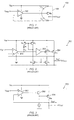
- Low drop-out regulator 100 includes an error amplifier 102 and a pass device 104 configured in a feedback arrangement.
- Error amplifier 102 is configured to drive a low current during DC conditions, and a high current, e.g., 1 mA, under high slew or transient conditions.
- Error amplifier typically comprises a class AB-type amplifier device.
- Error amplifier 102 has a positive input connected to a reference voltage V REF , and powered by an input supply voltage V IN .
- Reference voltage V REF which usually comprises a zener diode for high voltage applications or a bandgap reference for low voltage and high accuracy applications, is configured to provide a stable dc bias voltage with limited current driving capabilities.
- Pass device 104 comprises a power transistor device M P configured for driving an output current I OUT to a load device.
- Pass device 104 has a control terminal suitably coupled to the output of error amplifier 102 and can comprise various configurations, such as NPN follower, NMOS follower, or common emitter PNP or common source PMOS transistors.
- Bipolar devices are generally used for applications requiring higher output currents and are capable of generating higher quiescent currents, while MOS devices are generally used for applications requiring minimized quiescent current.
- the beta ⁇ is defined as the ratio of the collector current to base current. This base current can be large and is often driven into ground, i.e., the ground current is increased considerably.
- beta is also a measure of the efficiency, i.e., the ratio of the output current I OUT to the ground current. Because the bipolar device is considered a current gain device, the beta ⁇ can be quite low, ranging approximately from 100 to 1000. Thus, for every milliamp of current delivered at the output I OUT , 1 ⁇ A to 10 ⁇ A would be delivered to ground, i.e., for 100mA of output current, between 100 ⁇ A and 1000 ⁇ A of ground current are realized, resulting in poor efficiency for such bipolar devices.
- pass device 104 comprises a PMOS transistor device, which typically requires very low DC current under full load conditions.
- Pass device 104 receives at a control terminal, e.g., gate terminal, an amplified error signal from error amplifier 102 configured to control the output current flow of pass device 104 when driving the output load at an output terminal V OUT .
- Pass device 104 is configured to feed back the error signal to error amplifier 102.
- Pass device 104 also introduces large, parasitic capacitances C 1 and C 2 to low drop-out regulator 100.
- the large capacitances for example 100pF or more, can limit the capability of error amplifier 102, since the capacitances require high current during a fast transition.
- pass device 104 requires a large amount of current since parasitic capacitances C 1 and C 2 must be charged and discharged.
- milliamps of current during microsecond periods must be supplied by error amplifier 102 just to charge parasitic capacitances C 1 and C 2 .
- error amplifier 102 In addition to the requirement for higher current during transient conditions, other constraints are present on error amplifier 102. For example, as currently available power systems are demanding the use of less operating supply voltage V IM , such as an operating voltage of 1.8 volts, low drop-out regulator has to operate within one gate-source voltage V GS , or approximately within a threshold voltage V T of the pass device plus an extra voltage ⁇ . Thus for a single gate-source voltage V GS topology, to turn on pass device 104 with a threshold voltage V T of 0.7 to 1.2 volts, error amplifier 102 must provide at least that voltage plus the extra voltage ⁇ , all within the limited headroom of 1.8 volts.
- error amplifier 102 Another constraint on error amplifier 102 is the need to control the offset of the low drop-out regulator. In other words, not only does error amplifier 102 need to comprise a class AB device that can drive a lot of output current, while also providing a low quiescent current during low voltages, error amplifier 102 also needs to minimize the offset contribution.
- pass device 104 includes large parasitic capacitances, thus often requiring the implementation of a buffer, or a g m boost, to isolate the high output resistance of the gain stage of error amplifier 102 from the high load capacitance of pass device 104.
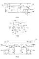
- a low drop-out regulator 200 implementing a buffer 206 between the output of an error amplifier 202 and a pass device 204 is illustrated.
- Buffer 206 is configured to receive the output current from error amplifier 202 and drive the gate of pass device 204.
- the output from buffer 206 can be mirrored back through a complex, current mirror circuit comprising transistors M 1 through M 5 to compensate error amplifier 202.
- low drop-out regulator 200 generally has a lower efficiency due to a higher ground current, i.e., the current mirror circuit comprising transistors M 1 through M s tends to drive current to ground.
- a buffer 306 can comprise a bipolar follower configuration, which is biased in class A operation.
- current is being taken from the supply and driven into ground, i.e., the ground current is increased considerably, resulting in reduced efficiency.
- NPN follower device 306 needs to be at least a base-emitter voltage V BE above the drive voltage, i.e., level shifting of the voltage at the gate of pass device 304 is necessary.
- V BE base-emitter voltage
- very little headroom is available for lower voltage power supply circuits, such as those with supply voltages V IN of 1.8 volts.
- control of pass device 304 can be difficult.
- a low drop-out regulator is configured to provide high output current with a fast response during transient conditions, while also maintaining low quiescent current under DC conditions.
- an exemplary low drop-out regulator comprises an error amplifier, a current feedback amplifier, and a pass device.
- the low drop-out regulator includes a composite amplifier feedback configuration, with the current feedback amplifier being decoupled from the overall composite feedback configuration and configured to provide effective compensation.
- the current feedback amplifier can be configured to operate with low current supplied from the error amplifier and to drive the control terminal of the pass device with sufficiently high current as demanded by a load device.
- the current feedback amplifier can be configured to permit the voltage at the control terminal of the pass device to operate from rail-to-rail.
- the current feedback amplifier instead of providing the feedback and reference signals into the high impedance control terminals of a pair of input devices, the current feedback amplifier is configured with a feedback and/or reference signal being provided to the low impedance input terminals of a pair of input devices.
- current is forced through the pair of input devices and can be suitably utilized to supply the low drop-out regulator with the ability to provide rail-to-rail output drive capabilities from an output device of the current feedback amplifier to the pass device.
- the gain and offset of the low drop-out regulator can be provided by the error amplifier, without the requirement to drive a high amount of current to the current feedback amplifier.
- the present invention may be described herein in terms of various functional components and various processing steps. It should be appreciated that such functional components may be realized by any number of hardware or structural components configured to perform the specified functions.
- the present invention may employ various integrated components, such as buffers, current mirrors, and logic devices comprised of various electrical devices, e.g., resistors, transistors, capacitors, diodes and the like, whose values may be suitably configured for various intended purposes.
- the present invention may be practiced in any integrated circuit application.
- exemplary embodiments of the present invention will be described herein in connection with a low drop-out regulator for use with power supply circuits.
- connections and couplings can be realized by direct connection between components, or by connection through other components and devices located thereinbetween.
- a low drop-out regulator is configured to provide high output current with a fast response during transient conditions, while also maintaining low quiescent current.
- an exemplary low drop-out regulator comprises an error amplifier, a current feedback amplifier, and a pass device.
- the low drop-out regulator includes a composite amplifier feedback configuration, with the current feedback amplifier being decoupled from the overall composite feedback configuration.
- the current feedback amplifier can be configured to operate with low current supplied from the error amplifier and to drive the gate of the pass device with sufficiently high current as demanded by a load device.
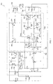
- Low drop-out regulator 400 in accordance with an exemplary embodiment of the present invention is illustrated.
- Low drop-out regulator 400 suitably comprises an error amplifier 402, a pass device 404, a current feedback amplifier 406, and a divider network 408.
- Low drop-out regulator 400 includes a composite amplifier feedback configuration, with the feedback loop of current feedback amplifier 406 being decoupled from the overall composite feedback loop, and with current feedback amplifier 406 being configured to provide effective compensation.
- error amplifier 402 suitably comprises a class A device configured to control the gain and offset of low drop-out regulator 400.
- Error amplifier 402 includes a non-inverting input terminal configured to receive a reference voltage, such as a bandgap reference voltage V BG , and a negative input terminal configured to receive a composite feedback signal from resistor network 408 through a resistor device R C .
- a capacitor C C is coupled from the output of error amplifier 402 to the negative input terminal of error amplifier 402.
- Capacitor C C can also be configured to supply additional current to the input of current feedback amplifier 406 to facilitate the driving of the control terminal of pass device 404 during transient conditions, e.g., for driving of the control terminal of pass device 404 to ground when the output voltage at output terminal V OUT is pulled down.
- error amplifier 402 is not required to drive a large amount of current to operate current feedback amplifier 406.
- Current feedback amplifier 406 is configured to operate with low current from error amplifier 402 and to suitably drive the control terminal of pass device 404.
- current feedback amplifier 406 is configured to receive an output signal from error amplifier 402 at an inverting input terminal.
- Current feedback amplifier also comprises a unity gain buffer configured with pass device 404 and a local feedback loop coupled from an output of pass device 404 to a non-inverting input terminal, i.e., a current feedback loop decoupled from the composite amplifier loop.
- current feedback amplifier 406 can be configured in various circuit arrangements for driving pass device 404.
- Pass device 404 comprises a power transistor device configured for driving an output current I OUT to a load device.
- pass device 404 comprises a PMOS transistor device having a source coupled to a supply voltage rail V S . a drain coupled to a output voltage terminal V OUT , and a control terminal, i.e., a gate, coupled to the output of current feedback amplifier 406.
- pass device can comprise any power transistor configuration, such as NPN or NMOS follower transistors, or any other transistor configuration for driving output current I OUT to a load device.
- Pass device 404 is configured to source as much current as needed by the load device and/or divider network 408.
- Divider network 408 suitably comprises a resistive divider configured for providing a composite feedback signal.
- divider network 408 comprises a pair of resistors R D1 and R D2 .
- Resistor R D1 is coupled between pass device 404 and resistor R D2 , while resistor R D2 is connected to ground.
- a composite feedback signal can be provided from a node V FDBK configured between resistors R D1 and R D2 , through resistor R C to the inverting input terminal of error amplifier 402.
- error amplifier 402 is configured to provide an output voltage equal to the voltage at output voltage terminal V OUT , and a low output current, to the inverting input terminal of current feedback amplifier 406.
- current feedback amplifier 406 is configured to provide a high output current to drive pass device 404, while only receiving a low input current from error amplifier 402 and a high transient current provided by capacitor C C .
- the current error amplifier can be configured to permit the voltage at the control terminal of the pass device, e.g., the gate voltage of a PMOS transistor device M P , to operate from rail-to-rail.
- the control terminal of the pass device e.g., the gate voltage of a PMOS transistor device M P
- V BG and V FDBK feedback voltage
- Each of PMOS devices 506 and 508, as well as output device 502 include large, parasitic capacitances that need to be charged to facilitate driving of current through a current mirror comprising transistor 501 and 503 to the gate of pass device 502.
- each of PMOS devices 506 and 508, as well as pass device 502 are configured as large transistor devices, such as 10x devices.
- the large capacitances tend to limit the amount of current that can be driven on the output.
- the amount of output current that can be driven is also limited by a current source 512 configured at the drain of PMOS device 502.
- a current feedback amplifier is configured with a feedback and/or reference signal being provided to the low impedance source terminals of a pair of input devices.
- current is forced through the pair of input devices and can be suitably utilized to supply the low drop-out regulator with the ability to provide fast, rail-to-rail output drive capabilities from an output device of the current feedback amplifier to the pass device.
- Current feedback amplifier 600 is configured to provide a fast response while also being configured to drive large amounts of current to a pass device.
- current feedback amplifier 600 can facilitate rail-to-rail operation of the gate of the pass device.
- Current feedback amplifier 600 suitably comprises a pair of input transistor devices 602 and 604, a pair of diode connected devices 606 and 608, a pair of lower current mirrors 610 and 616, a pair of current sources 626 and 628, and upper rail current mirror 620.
- Input transistor devices 602 and 604 are configured for receiving input current signals, such as from voltage terminals V PP (+) and V NN (-), at their sources, respectively, with the source of input transistor device 602 comprising the positive or non-inverting input terminal and the source of input transistor device 604 comprising the negative or inverting input terminal of current feedback amplifier 600.
- the source of input transistor device 602 can be coupled to the output of the pass device in a feedback arrangement, and the source of input transistor device 604 can be coupled to the output of the error amplifier.
- Input device 602 has a gate coupled to a gate of a diode-connected transistor device 606, while input device 604 has a gate coupled to a gate of a diode-connected transistor device 608.
- input device 602 has a drain coupled to current mirror 610
- input device 604 has a drain coupled to current mirror 616.
- Diode-connected devices 606 and 608 are configured to facilitate control of the flow of current through input devices 602 and 604.
- Diode-connected devices 606 and 608 are configured to control the gates of input devices 602 and 604 in a fixed manner such that any current flowing input current signals, such as from voltage terminals V PP (+) and V NN (-), will be directed through input devices 602 and 604, respectively.
- Diode-connected device 606 has source coupled to input voltage signal V NN (-) similar to the connection of the source of input device 604, and a drain coupled to ground through a current source 626
- diode-connected device 608 has a source coupled to input voltage signal V PP (+) similar to the connection of the source of input device 602, and a drain coupled to ground through a current source 628. While diode-connected devices 606 and 608 can be configured at approximately the same transistor device size as input devices 602 and 604, in accordance with the exemplary embodiment, input devices 602 and 604 are approximately two times the transistor size of devices 606 and 608.
- Current sources 626 and 628 are configured to provide a fixed current flowing through diode-connected devices 606 and 608, and can comprise various current source configurations.
- Current sources 626 and 628 are configured to operate with a low current, for example, approximately 2 ⁇ A of current, which can flow through diode-connected devices 606 and 608.
- This low amount of current flowing through diode-connected devices 606 and 608 operates to hold input devices 602 and 604 at a low queue current, i.e., under DC conditions.
- input devices 602 and 604 can realize 4 ⁇ A of current flowing through each under DC conditions.
- Current mirrors 610 and 616 are configured to mirror the current flowing through transistors 602 and 604, and provide the mirrored current to upper rail current mirror 620, a diode-connected transistor 622 and an upper output device 624 configured at the upper rail of current feedback amplifier 600.
- Current mirror 610 comprises a diode-connected transistor 614 having a drain coupled to input device 602, and a transistor 612 having a gate coupled to a gate of transistor 614, and a drain coupled to upper transistor 622.
- current mirror 616 comprises a diode-connected transistor 618 having a drain coupled to input device 604, and a lower output device 620 having a gate coupled to a gate of transistor 618, and a drain coupled to upper output device 624.
- Upper rail transistors 622 and 624 are configured to provide an output current to the pass device of the low drop-out regulator.
- Diode-connected transistor 622 is configured to suitably mirror any current received from current mirror 610 to the control terminal of the pass device through the drain of transistor 624, which comprises the upper output device for current feedback amplifier 600.
- upper output device 624 is approximately four times the transistor size of upper rail transistor 622, e.g., an 8X device size for output device 624 and a 2X device size for transistor 622.
- Lower output device 620 is also sized approximately four times the transistor size of lower rail transistor 618.
- current feedback amplifier 600 is configured to operate with a very low queue current in input devices 602 and 604 under DC conditions. However, instead of providing additional current received from a feedback signal directly to ground, such as that of error amplifier 500, current feedback amplifier 600 can supply additional current through the output devices 622 and 624 to a pass device under slewing conditions, i.e., when the output load requires additional current during transitions.
- Low drop-out regulator 700 comprises an error amplifier 702, a pass device 704, a current feedback amplifier 706, and a divider network 708.
- Low drop-out regulator 700 is suitably configured with a composite feedback loop, with the feedback loop of current feedback amplifier 706 being decoupled from the overall composite feedback loop.
- error amplifier 702 suitably comprises a class A device configured to control the gain and offset of low drop-out regulator 700.
- Error amplifier 702 includes a differential pair of transistors 710 and 712, a current source circuit 726, and an output device 724.
- Transistor 712 has a gate configured as a positive input terminal coupled to a reference voltage V REF , such as a bandgap reference voltage, e.g., a bandgap voltage of approximately 1.2 volts.
- Transistor 710 has a gate configured as a negative input terminal configured to receive a composite feedback signal from resistor network 708.
- Source terminals of transistors 710 and 712 are connected together within the differential pair configuration, and are coupled to a current source 716.
- Drains of differential pair of transistors 710 and 712 can be coupled to a gate of output transistor 724 through a current mirror comprising transistors 720 and 722.
- output current from input transistor 710 can be suitably mirrored through diode-connected transistor 720 and transistor 722 to the gate of output transistor 724, while output current from input transistor 712 can be directly connected to drive the gate of output transistor 724.
- a composite amplifier feedback loop can be provided from divider network 708 through a resistor device R C to the negative terminal of error amplifier 702, i.e., to the gate of input transistor 710.
- Resistor device R C can comprise various resistance values to effectively vary the compensation to error amplifier 702.
- error amplifier 702 can comprise a capacitor C C coupled between the negative terminal of error amplifier 702, i.e., to the gate of input transistor 710, and the drain of output device 724 to suitably supply additional current to facilitate the driving of the gate of pass device 704 during transient conditions, e.g., for driving of the gate of pass device 704 to ground when the output voltage at output terminal V OUT is pulled down.
- Capacitor C C can vary in capacitance level between approximately 1Op to 100pF, with the higher the value of capacitance, the lower the value of resistance of resistor R E .
- resistor device R C can comprise an active variance device, while capacitor C C comprises a fixed capacitance of approximately 20pF.
- a supply voltage V S is suitably configured to supply voltage to the upper supply rail.
- Supply voltage V S can comprise various levels of supply voltage, such as 2.8 volts, that provides additional headroom. However, supply voltage V S can also comprise a significantly lower voltage supply, such as 1.8 volts, and yet have sufficient headroom for operation of low drop-out regulator 700.
- Current source device 726 is configured to drive a plurality of current sources 716, 718, 626 and 628.
- Current source device 726 can comprise various types and configurations of current source devices for driving a plurality of current sources.
- error amplifier 702 can include a diode-connected transistor device 714 configured to mirror current from current source device 726 to current sources 716, 718, 626 and 628. As explained above with respect to current feedback amplifier 600, due to the operation of current sources 626 and 628, error amplifier 702 is not required to drive a large amount of current to operate current feedback amplifier 706.
- Current feedback amplifier 706 is configured to operate with low current from error amplifier 702 and to suitably drive the gate of pass device 704.
- current feedback amplifier 406 comprises an amplifier similar to that of current feedback amplifier 600.
- current feedback amplifier 706 can also be configured in various other circuit arrangements configured for driving pass device 704.
- input device 602 has a source coupled through input terminal V PP (+) to output terminal V OUT and to pass device 704, while input device 604 has a source coupled through input terminal V NN (-) to output device 724 of error amplifier 702.
- Pass device 704 comprises a power transistor device configured for driving an output current I OUT to a load device.
- pass device 704 comprises a PMOS transistor device having a source coupled to a supply voltage rail V S , and a drain coupled to a output voltage terminal V OUT .
- pass device can comprise any power transistor configuration for driving output current I OUT to a load device.
- pass device 704 is configured to source as much current as needed by the load device and/or divider network 708.
- Divider network 708 suitably comprises a resistive divider configured for providing a composite feedback signal.
- divider network 708 comprises a pair of resistors R D1 and R D2 .
- divider network 708 can comprise any configuration of resistors for providing a voltage divider operation.
- Resistor R D1 is coupled between pass device 704 and resistor R D2 , while resistor R D2 is connected to ground.
- a composite feedback signal can be provided from a node V FDBK configured between resistors R D1 and R D2 , to the negative input terminal of error amplifier 702, i.e., to the gate of input transistor 710.
- the positive input terminal of current feedback amplifier 706, i.e., the source of input transistor 602, is coupled in a feedback arrangement to the output terminal V OUT and to the drain of pass device 704.
- diode-connected devices 606 and 608 are configured to control input devices 602 and 604 such that any current signals appearing at input terminals V PP (+) and V NN , (-) will flow through input devices 602 and 604, respectively.
- low drop-out regulator 700 For example when the output voltage at terminal V OUT increases rapidly, such as when an output load is turned off rapidly to release the output voltage upwards, current amplifier 706 operates to drive node V GATE of pass device 704 to the upper rail supply V S .
- pass device 704 will suitably drive a higher current into input device 602 through input terminal V PP (+).
- the higher current flowing through input device 602 can be suitably mirrored through current mirror 610 to upper rail device 622, turning on output device 624, pulling up node V GATE very rapidly towards supply rail V S .
- Node 632 tracks the rise in V PP (+), since the gate-source voltage V GS of device 608 remains fixed.
- the gate-source voltage V GS of device 604 decreases, effectively shutting off lower output device 620, releasing node V GATE to rise even closer to the upper supply rail V S .
- the rising voltage at terminal V OUT is divided down by R D1 and R D2 .
- the V FDBK node also rises, causing the output device 724 of error amplifier 702 to shut off rapidly, thus causing the voltage at input terminal V NN (-) to decrease.
- the current driven through input device 604 is further reduced, releasing node V GATE to rise even closer to the upper supply rail V S .
- Node 630 tracks the decrease in V NN (-), since the gate-source voltage V GS of device 606 remains fixed.
- the gate-source voltage V GS of device 602 increases, further increasing the current through device 602, which is suitably mirrored through current mirror 610 to the upper rail device 622, further turning on output device 624 to pull up the gate of pass device 704.
- pass device 704 will suitably drive a lower current into input device 602 through input terminal V PP (+).
- the lower current flowing through input device 602 can be suitably mirrored through current mirror 610 to upper rail device 622, effectively turning off output device 624, releasing node V GATE to fall to ground.
- Node 632 tracks the fall in V PP (+), since the gate-source voltage Vgs of device 608 remains fixed.
- the gate-source voltage V GS of device 604 increases, turning on lower output device 620, pulling down node V GATE very rapidly towards ground.
- the decreasing voltage at terminal V OUT is divided down by R D1 and R D2 .
- the V FDBK node also decreases, causing the output device 724 of error amplifier 702 to turn on rapidly, causing the voltage at input terminal V NN (-) to increase.
- the current driven through input device 604 is further increased, pulling down node V GATE even closer to ground.
- Node 630 tracks the increase in V NN (-), since the gate-source voltage V GS of device 606 remains fixed.
- the gate-source voltage V GS of device 602 decreases, further decreasing the current through device 602, which is suitably mirrored through current mirror 610 to the upper rail device 622, further turning off output device 624, thus releasing node V GATE to fall to even closer to ground.
- the high current provided to the gate of pass device 704 suitably enables any parasitic capacitances within pass device 704 to be rapidly charged and discharged without impairing the operation of error amplifier 702 and current feedback amplifier 706.
- the gate of pass device 704 can be suitably driven to the upper rail and ground, i.e., rail-to-rail, with the current supplied by current feedback amplifier 706.
- current feedback amplifier 706 can suitably utilize current, rather than voltage, to charge and discharge the parasitic capacitances very rapidly.
- current feedback amplifier 706 can suitably receive an input current, convert that current into a voltage, and then convert the voltage back to a current for output to drive the pass device.
- current feedback amplifier 706 does not require a high input voltage or high input current for operation. Instead, a low voltage less than 2 times the threshold voltage V T , can be provided to error amplifier 702 and current feedback amplifier 706. In addition, current feedback amplifier 706 can operate with only a few micro-amps of current, and yet can provide several milli-amps of output current very quickly to drive the gate of pass device 704.
- the gain of low drop-out regulator 700 can be relegated to error amplifier 702, which also controls the offset, and which does not need to drive a high amount of current to current feedback amplifier 706.
- the matching of the various transistor devices of current feedback amplifier 706, such as devices 602, 604, 606, 608, 612, 614, 618, 620, 622 and 624, and error amplifier 702, such as devices 710 and 712 is not critical to the operation of low drop-out regulator 700.
- the composite feedback configuration of error amplifier 702, which is configured to control the offset of low drop-out regulator 700 does not significantly affect the accuracy of the output of current feedback amplifier 706.
- transistor devices 710 and 712 can comprise 10x devices, while devices 602 and 604 (4x), devices 606 and 608 (2x), and devices 612 and 614 (1x) can comprise different sized devices without impacting the offset of low drop-out regulator 700.
Applications Claiming Priority (2)
| Application Number | Priority Date | Filing Date | Title |
|---|---|---|---|
| US151366 | 1998-09-11 | ||
| US10/151,366 US6703815B2 (en) | 2002-05-20 | 2002-05-20 | Low drop-out regulator having current feedback amplifier and composite feedback loop |
Publications (2)
| Publication Number | Publication Date |
|---|---|
| EP1365302A1 true EP1365302A1 (de) | 2003-11-26 |
| EP1365302B1 EP1365302B1 (de) | 2010-04-28 |
Family
ID=29400507
Family Applications (1)
| Application Number | Title | Priority Date | Filing Date |
|---|---|---|---|
| EP03101432A Expired - Fee Related EP1365302B1 (de) | 2002-05-20 | 2003-05-20 | Spannungsregulierungseinrichtung mit niedrigem Spannungsabfall |
Country Status (4)
| Country | Link |
|---|---|
| US (1) | US6703815B2 (de) |
| EP (1) | EP1365302B1 (de) |
| JP (1) | JP2004005670A (de) |
| DE (1) | DE60332300D1 (de) |
Cited By (12)
| Publication number | Priority date | Publication date | Assignee | Title |
|---|---|---|---|---|
| EP1835373A1 (de) | 2006-03-15 | 2007-09-19 | St Microelectronics S.A. | Erzeugung einer Bezugsspannung |
| EP1865397A1 (de) | 2006-06-05 | 2007-12-12 | St Microelectronics S.A. | Regler mit geringer Abschaltspannung |
| CN102707754A (zh) * | 2012-05-30 | 2012-10-03 | 昆山锐芯微电子有限公司 | 低压差线性稳压电路 |
| CN101727119B (zh) * | 2009-11-26 | 2013-09-04 | 四川和芯微电子股份有限公司 | 具有有效补偿的低压差线性电压源 |
| US8648578B2 (en) | 2007-09-30 | 2014-02-11 | Nxp, B.V. | Capless low drop-out voltage regulator having discharge circuit compensating for on-chip output capacitance and response time |
| CN103869860A (zh) * | 2012-12-13 | 2014-06-18 | 创杰科技股份有限公司 | 电压产生器 |
| US20140191739A1 (en) * | 2013-01-07 | 2014-07-10 | Samsung Electronics Co., Ltd. | Low drop-out regulator |
| EP2804067A1 (de) | 2013-05-17 | 2014-11-19 | Asahi Kasei Microdevices Corporation | Leistungsarmer LDO-Spannungsregler mit geringer Ausgangsrauschdichte |
| EP2952995A1 (de) * | 2014-06-04 | 2015-12-09 | Dialog Semiconductor (UK) Limited | Linearer Spannungsregler mit einem großen Bereich von Bypass-Kapazität |
| WO2018080697A1 (en) * | 2016-10-27 | 2018-05-03 | Qualcomm Incorporated | Voltage regulator with enhanced power supply rejection ratio and load-transient performance |
| CN111316188A (zh) * | 2018-09-26 | 2020-06-19 | 深圳市汇顶科技股份有限公司 | 一种低压差线性稳压系统 |
| CN111596118A (zh) * | 2020-06-23 | 2020-08-28 | 上海安路信息科技有限公司 | 电流检测电路及低压差稳压器电路 |
Families Citing this family (90)
| Publication number | Priority date | Publication date | Assignee | Title |
|---|---|---|---|---|
| DE10249162B4 (de) * | 2002-10-22 | 2007-10-31 | Texas Instruments Deutschland Gmbh | Spannungsregler |
| US6836101B2 (en) * | 2002-12-05 | 2004-12-28 | Comarco Wireless Technologies, Inc. | Tip having active circuitry |
| US6806693B1 (en) * | 2003-04-14 | 2004-10-19 | National Semiconductor Corporation | Method and system for improving quiescent currents at low output current levels |
| US7872454B2 (en) * | 2003-08-21 | 2011-01-18 | Marvell World Trade Ltd. | Digital low dropout regulator |
| US7760525B2 (en) * | 2003-08-21 | 2010-07-20 | Marvell World Trade Ltd. | Voltage regulator |
| US7002326B1 (en) * | 2003-09-08 | 2006-02-21 | National Semiconductor Corporation | Method of modulating current regulation control loop's current magnitude from a second control signal |
| US9153960B2 (en) | 2004-01-15 | 2015-10-06 | Comarco Wireless Technologies, Inc. | Power supply equipment utilizing interchangeable tips to provide power and a data signal to electronic devices |
| US6933772B1 (en) * | 2004-02-02 | 2005-08-23 | Freescale Semiconductor, Inc. | Voltage regulator with improved load regulation using adaptive biasing |
| US8324872B2 (en) * | 2004-03-26 | 2012-12-04 | Marvell World Trade, Ltd. | Voltage regulator with coupled inductors having high coefficient of coupling |
| US7368896B2 (en) * | 2004-03-29 | 2008-05-06 | Ricoh Company, Ltd. | Voltage regulator with plural error amplifiers |
| US7095257B2 (en) * | 2004-05-07 | 2006-08-22 | Sige Semiconductor (U.S.), Corp. | Fast low drop out (LDO) PFET regulator circuit |
| US7190152B2 (en) * | 2004-07-13 | 2007-03-13 | Marvell World Trade Ltd. | Closed-loop digital control system for a DC/DC converter |
| FR2873216A1 (fr) * | 2004-07-15 | 2006-01-20 | St Microelectronics Sa | Circuit integre avec regulateur modulable a faible chute de tension |
| US7205828B2 (en) * | 2004-08-02 | 2007-04-17 | Silicon Laboratories, Inc. | Voltage regulator having a compensated load conductance |
| TWI263124B (en) * | 2004-11-19 | 2006-10-01 | Sunplus Technology Co Ltd | Voltage regulator circuit with low quiescent current |
| US7135842B2 (en) * | 2005-01-31 | 2006-11-14 | Freescale Semiconductor, Inc. | Voltage regulator having improved IR drop |
| US7218083B2 (en) * | 2005-02-25 | 2007-05-15 | O2Mincro, Inc. | Low drop-out voltage regulator with enhanced frequency compensation |
| US7656224B2 (en) * | 2005-03-16 | 2010-02-02 | Texas Instruments Incorporated | Power efficient dynamically biased buffer for low drop out regulators |
| US7170269B1 (en) * | 2005-05-16 | 2007-01-30 | National Semiconductor Corporation | Low dropout regulator with control loop for avoiding hard saturation |
| TW200642246A (en) * | 2005-05-20 | 2006-12-01 | Richtek Technology Corp | DC buck/boost converter |
| US7301316B1 (en) * | 2005-08-12 | 2007-11-27 | Altera Corporation | Stable DC current source with common-source output stage |
| DE102005039114B4 (de) * | 2005-08-18 | 2007-06-28 | Texas Instruments Deutschland Gmbh | Spannungsregler mit einem geringen Spannungsabfall |
| US7466115B2 (en) * | 2005-09-19 | 2008-12-16 | Texas Instruments Incorporated | Soft-start circuit and method for power-up of an amplifier circuit |
| US7659703B1 (en) * | 2005-10-14 | 2010-02-09 | National Semiconductor Corporation | Zero generator for voltage regulators |
| US7417416B2 (en) * | 2005-10-27 | 2008-08-26 | International Business Machines Corporation | Regulator with load tracking bias |
| KR100713995B1 (ko) * | 2005-11-07 | 2007-05-04 | 삼성에스디아이 주식회사 | Dcdc 변환기 및 그를 이용한 유기발광표시장치 |
| TW200744284A (en) * | 2006-05-24 | 2007-12-01 | Asustek Comp Inc | Voltage regulating circuit with over-current protection |
| US7642754B2 (en) * | 2006-06-08 | 2010-01-05 | Semiconductor Components Industries, L.L.C. | Method of forming a voltage regulator and structure therefor |
| JP4966592B2 (ja) * | 2006-06-09 | 2012-07-04 | ローム株式会社 | 電源回路 |
| JP4866158B2 (ja) * | 2006-06-20 | 2012-02-01 | 富士通セミコンダクター株式会社 | レギュレータ回路 |
| US7919954B1 (en) * | 2006-10-12 | 2011-04-05 | National Semiconductor Corporation | LDO with output noise filter |
| US8294441B2 (en) * | 2006-11-13 | 2012-10-23 | Decicon, Inc. | Fast low dropout voltage regulator circuit |
| US20080136384A1 (en) * | 2006-12-06 | 2008-06-12 | Texas Instruments, Incorporated | Capacitor-free linear voltage regulator for integrated controller area network transceivers |
| US8304931B2 (en) | 2006-12-18 | 2012-11-06 | Decicon, Inc. | Configurable power supply integrated circuit |
| JP2008217677A (ja) * | 2007-03-07 | 2008-09-18 | Ricoh Co Ltd | 定電圧回路及びその動作制御方法 |
| US7570035B2 (en) * | 2007-08-01 | 2009-08-04 | Zerog Wireless, Inc. | Voltage regulator with a hybrid control loop |
| US8174251B2 (en) * | 2007-09-13 | 2012-05-08 | Freescale Semiconductor, Inc. | Series regulator with over current protection circuit |
| US7777465B2 (en) * | 2007-11-15 | 2010-08-17 | Macronix International Co. Ltd | Output transient responsive voltage regulator controlling apparatus and method |
| US7863884B1 (en) * | 2008-01-09 | 2011-01-04 | Intersil Americas Inc. | Sub-volt bandgap voltage reference with buffered CTAT bias |
| US8710813B2 (en) * | 2008-04-11 | 2014-04-29 | System General Corp. | Low drop-out regulator providing constant current and maximum voltage limit |
| US8278893B2 (en) | 2008-07-16 | 2012-10-02 | Infineon Technologies Ag | System including an offset voltage adjusted to compensate for variations in a transistor |
| US20100066326A1 (en) * | 2008-09-16 | 2010-03-18 | Huang Hao-Chen | Power regulator |
| TW201013354A (en) * | 2008-09-19 | 2010-04-01 | Numen Technology Inc | Structure of fixed-current device which can be connected in series, application circuit and operation method of same |
| US7994764B2 (en) * | 2008-11-11 | 2011-08-09 | Semiconductor Components Industries, Llc | Low dropout voltage regulator with high power supply rejection ratio |
| IT1392262B1 (it) * | 2008-12-15 | 2012-02-22 | St Microelectronics Des & Appl | "regolatore lineare di tipo low-dropout con efficienza migliorata e procedimento corrispondente" |
| TW201044132A (en) * | 2009-06-03 | 2010-12-16 | Advanced Analog Technology Inc | Quick-start low dropout regulator |
| US8754620B2 (en) * | 2009-07-03 | 2014-06-17 | Stmicroelectronics International N.V. | Voltage regulator |
| CN101963820B (zh) * | 2009-07-21 | 2013-11-06 | 意法半导体研发(上海)有限公司 | 自适应密勒补偿型电压调节器 |
| JP5494177B2 (ja) | 2010-04-21 | 2014-05-14 | 富士通株式会社 | 半導体装置 |
| US20120019227A1 (en) * | 2010-07-23 | 2012-01-26 | Panasonic Semiconductor Asia Pte., Ltd. | Power supply circuit |
| US8482266B2 (en) * | 2011-01-25 | 2013-07-09 | Freescale Semiconductor, Inc. | Voltage regulation circuitry and related operating methods |
| US8710809B2 (en) * | 2011-06-28 | 2014-04-29 | Stmicroelectronics International N.V. | Voltage regulator structure that is operationally stable for both low and high capacitive loads |
| US9240690B2 (en) | 2011-09-08 | 2016-01-19 | Agency For Science, Technology And Research | Power transfer device |
| KR101932519B1 (ko) * | 2011-11-14 | 2018-12-27 | 삼성전자 주식회사 | 휴대 단말기의 근접 인터페이스 커플링 카드 선택 방법 및 장치 |
| US20130119954A1 (en) * | 2011-11-16 | 2013-05-16 | Iwatt Inc. | Adaptive transient load switching for a low-dropout regulator |
| CN102393781A (zh) * | 2011-12-06 | 2012-03-28 | 四川和芯微电子股份有限公司 | 低压差线性稳压电路及系统 |
| US9134743B2 (en) | 2012-04-30 | 2015-09-15 | Infineon Technologies Austria Ag | Low-dropout voltage regulator |
| US9122293B2 (en) | 2012-10-31 | 2015-09-01 | Qualcomm Incorporated | Method and apparatus for LDO and distributed LDO transient response accelerator |
| US9170590B2 (en) | 2012-10-31 | 2015-10-27 | Qualcomm Incorporated | Method and apparatus for load adaptive LDO bias and compensation |
| US9235225B2 (en) | 2012-11-06 | 2016-01-12 | Qualcomm Incorporated | Method and apparatus reduced switch-on rate low dropout regulator (LDO) bias and compensation |
| US8981745B2 (en) | 2012-11-18 | 2015-03-17 | Qualcomm Incorporated | Method and apparatus for bypass mode low dropout (LDO) regulator |
| TWI516895B (zh) * | 2013-10-04 | 2016-01-11 | 慧榮科技股份有限公司 | 低壓差穩壓裝置以及緩衝級電路 |
| US9195248B2 (en) | 2013-12-19 | 2015-11-24 | Infineon Technologies Ag | Fast transient response voltage regulator |
| JP6261349B2 (ja) * | 2014-01-22 | 2018-01-17 | エスアイアイ・セミコンダクタ株式会社 | ボルテージレギュレータ |
| JP6312492B2 (ja) * | 2014-03-27 | 2018-04-18 | ラピスセミコンダクタ株式会社 | 半導体装置及び電流源制御方法 |
| KR102204678B1 (ko) * | 2014-12-11 | 2021-01-20 | 삼성전자주식회사 | 인버터 증폭기 기반의 이중 루프 레귤레이터 및 그에 따른 전압 레귤레이팅 방법 |
| US9588531B2 (en) * | 2015-05-16 | 2017-03-07 | Nxp Usa, Inc. | Voltage regulator with extended minimum to maximum load current ratio |
| US10558232B2 (en) | 2015-05-26 | 2020-02-11 | Sony Corporation | Regulator circuit and control method |
| CN105116951B (zh) * | 2015-06-23 | 2017-06-06 | 北京兆易创新科技股份有限公司 | 一种电压输出方法和装置 |
| TWI560538B (en) * | 2015-06-30 | 2016-12-01 | Univ Nat Tsing Hua | Feedback type voltage regulator |
| KR102395466B1 (ko) * | 2015-07-14 | 2022-05-09 | 삼성전자주식회사 | 리플 감소 속도를 제고한 레귤레이터 회로 |
| US9899912B2 (en) * | 2015-08-28 | 2018-02-20 | Vidatronic, Inc. | Voltage regulator with dynamic charge pump control |
| US9971370B2 (en) * | 2015-10-19 | 2018-05-15 | Novatek Microelectronics Corp. | Voltage regulator with regulated-biased current amplifier |
| KR102369532B1 (ko) | 2015-10-29 | 2022-03-03 | 삼성전자주식회사 | 레귤레이터 회로 |
| US10224876B2 (en) | 2015-12-08 | 2019-03-05 | Skyworks Solutions, Inc. | Low dropout voltage regulator for highly linear radio frequency power amplifiers |
| US9836071B2 (en) | 2015-12-29 | 2017-12-05 | Silicon Laboratories Inc. | Apparatus for multiple-input power architecture for electronic circuitry and associated methods |
| US9964986B2 (en) | 2015-12-29 | 2018-05-08 | Silicon Laboratories Inc. | Apparatus for power regulator with multiple inputs and associated methods |
| US11009900B2 (en) | 2017-01-07 | 2021-05-18 | Texas Instruments Incorporated | Method and circuitry for compensating low dropout regulators |
| US11009901B2 (en) * | 2017-11-15 | 2021-05-18 | Qualcomm Incorporated | Methods and apparatus for voltage regulation using output sense current |
| US11099591B1 (en) | 2018-09-11 | 2021-08-24 | University Of South Florida | Method and apparatus for mitigating performance degradation in digital low-dropout voltage regulators (DLDOs) caused by limit cycle oscillation (LCO) and other factors |
| US11493945B1 (en) | 2018-12-30 | 2022-11-08 | University Of South Florida | Method and apparatus for mitigating performance degradation in digital low-dropout voltage regulators (DLDOs) |
| US10775819B2 (en) * | 2019-01-16 | 2020-09-15 | Avago Technologies International Sales Pte. Limited | Multi-loop voltage regulator with load tracking compensation |
| CN110989756B (zh) * | 2019-12-05 | 2021-07-30 | 思瑞浦微电子科技(苏州)股份有限公司 | 基于恒定功率保护的低压差线性稳压器 |
| CN113703507B (zh) * | 2020-05-23 | 2023-01-10 | 圣邦微电子(北京)股份有限公司 | 一种提高ldo响应速度电路 |
| US11635778B2 (en) | 2020-09-25 | 2023-04-25 | Apple Inc. | Voltage regulator circuit |
| KR102398518B1 (ko) * | 2020-12-29 | 2022-05-17 | 에스케이하이닉스 주식회사 | LDO(Low-Dropout) 선형 레귤레이터 |
| TWI801922B (zh) * | 2021-05-25 | 2023-05-11 | 香港商科奇芯有限公司 | 電壓調節器 |
| CN116136701A (zh) | 2021-11-17 | 2023-05-19 | 科奇芯有限公司 | 电压调节电路 |
| TWI800223B (zh) * | 2021-11-17 | 2023-04-21 | 香港商科奇芯有限公司 | 低通濾波電路 |
| CN114189148B (zh) * | 2022-01-21 | 2022-10-21 | 钰泰半导体股份有限公司 | 功率转换器及其控制方法 |
Citations (4)
| Publication number | Priority date | Publication date | Assignee | Title |
|---|---|---|---|---|
| US5365161A (en) * | 1991-11-26 | 1994-11-15 | Rohm Co., Ltd. | Stabilized voltage supply |
| US5563501A (en) * | 1995-01-20 | 1996-10-08 | Linfinity Microelectronics | Low voltage dropout circuit with compensating capacitance circuitry |
| EP0957421A2 (de) * | 1998-05-13 | 1999-11-17 | Texas Instruments Incorporated | Stromeffiziente Regelungseinichtung mit kleiner Verlustspannung, verbesserter Lasregelung und Frequenzgang |
| EP1253498A1 (de) * | 2001-04-24 | 2002-10-30 | Infineon Technologies AG | Spannungsregler |
Family Cites Families (8)
| Publication number | Priority date | Publication date | Assignee | Title |
|---|---|---|---|---|
| US5191278A (en) * | 1991-10-23 | 1993-03-02 | International Business Machines Corporation | High bandwidth low dropout linear regulator |
| US5559424A (en) * | 1994-10-20 | 1996-09-24 | Siliconix Incorporated | Voltage regulator having improved stability |
| US5861736A (en) * | 1994-12-01 | 1999-01-19 | Texas Instruments Incorporated | Circuit and method for regulating a voltage |
| US6246221B1 (en) * | 2000-09-20 | 2001-06-12 | Texas Instruments Incorporated | PMOS low drop-out voltage regulator using non-inverting variable gain stage |
| JP4640739B2 (ja) * | 2000-11-17 | 2011-03-02 | ローム株式会社 | 安定化直流電源装置 |
| US6518737B1 (en) * | 2001-09-28 | 2003-02-11 | Catalyst Semiconductor, Inc. | Low dropout voltage regulator with non-miller frequency compensation |
| US6522112B1 (en) * | 2001-11-08 | 2003-02-18 | National Semiconductor Corporation | Linear regulator compensation inversion |
| US6465994B1 (en) * | 2002-03-27 | 2002-10-15 | Texas Instruments Incorporated | Low dropout voltage regulator with variable bandwidth based on load current |
-
2002
- 2002-05-20 US US10/151,366 patent/US6703815B2/en not_active Expired - Lifetime
-
2003
- 2003-05-19 JP JP2003140180A patent/JP2004005670A/ja active Pending
- 2003-05-20 EP EP03101432A patent/EP1365302B1/de not_active Expired - Fee Related
- 2003-05-20 DE DE60332300T patent/DE60332300D1/de not_active Expired - Lifetime
Patent Citations (4)
| Publication number | Priority date | Publication date | Assignee | Title |
|---|---|---|---|---|
| US5365161A (en) * | 1991-11-26 | 1994-11-15 | Rohm Co., Ltd. | Stabilized voltage supply |
| US5563501A (en) * | 1995-01-20 | 1996-10-08 | Linfinity Microelectronics | Low voltage dropout circuit with compensating capacitance circuitry |
| EP0957421A2 (de) * | 1998-05-13 | 1999-11-17 | Texas Instruments Incorporated | Stromeffiziente Regelungseinichtung mit kleiner Verlustspannung, verbesserter Lasregelung und Frequenzgang |
| EP1253498A1 (de) * | 2001-04-24 | 2002-10-30 | Infineon Technologies AG | Spannungsregler |
Cited By (20)
| Publication number | Priority date | Publication date | Assignee | Title |
|---|---|---|---|---|
| EP1835373A1 (de) | 2006-03-15 | 2007-09-19 | St Microelectronics S.A. | Erzeugung einer Bezugsspannung |
| FR2898701A1 (fr) * | 2006-03-15 | 2007-09-21 | St Microelectronics Sa | Generation d'une tension de reference |
| EP1865397A1 (de) | 2006-06-05 | 2007-12-12 | St Microelectronics S.A. | Regler mit geringer Abschaltspannung |
| US8044653B2 (en) | 2006-06-05 | 2011-10-25 | Stmicroelectronics Sa | Low drop-out voltage regulator |
| US8648578B2 (en) | 2007-09-30 | 2014-02-11 | Nxp, B.V. | Capless low drop-out voltage regulator having discharge circuit compensating for on-chip output capacitance and response time |
| CN101727119B (zh) * | 2009-11-26 | 2013-09-04 | 四川和芯微电子股份有限公司 | 具有有效补偿的低压差线性电压源 |
| CN102707754B (zh) * | 2012-05-30 | 2014-08-13 | 昆山锐芯微电子有限公司 | 低压差线性稳压电路 |
| CN102707754A (zh) * | 2012-05-30 | 2012-10-03 | 昆山锐芯微电子有限公司 | 低压差线性稳压电路 |
| CN103869860A (zh) * | 2012-12-13 | 2014-06-18 | 创杰科技股份有限公司 | 电压产生器 |
| TWI470394B (zh) * | 2012-12-13 | 2015-01-21 | Issc Technologies Corp | 電壓產生器 |
| CN103869860B (zh) * | 2012-12-13 | 2016-09-07 | 密克罗奇普技术公司 | 电压产生器 |
| US9256237B2 (en) * | 2013-01-07 | 2016-02-09 | Samsung Electronics Co., Ltd. | Low drop-out regulator |
| US20140191739A1 (en) * | 2013-01-07 | 2014-07-10 | Samsung Electronics Co., Ltd. | Low drop-out regulator |
| EP2804067A1 (de) | 2013-05-17 | 2014-11-19 | Asahi Kasei Microdevices Corporation | Leistungsarmer LDO-Spannungsregler mit geringer Ausgangsrauschdichte |
| EP2952995A1 (de) * | 2014-06-04 | 2015-12-09 | Dialog Semiconductor (UK) Limited | Linearer Spannungsregler mit einem großen Bereich von Bypass-Kapazität |
| WO2018080697A1 (en) * | 2016-10-27 | 2018-05-03 | Qualcomm Incorporated | Voltage regulator with enhanced power supply rejection ratio and load-transient performance |
| CN111316188A (zh) * | 2018-09-26 | 2020-06-19 | 深圳市汇顶科技股份有限公司 | 一种低压差线性稳压系统 |
| CN111316188B (zh) * | 2018-09-26 | 2022-01-07 | 深圳市汇顶科技股份有限公司 | 一种低压差线性稳压系统 |
| CN111596118A (zh) * | 2020-06-23 | 2020-08-28 | 上海安路信息科技有限公司 | 电流检测电路及低压差稳压器电路 |
| CN111596118B (zh) * | 2020-06-23 | 2020-12-11 | 上海安路信息科技有限公司 | 电流检测电路及低压差稳压器电路 |
Also Published As
| Publication number | Publication date |
|---|---|
| US20030214275A1 (en) | 2003-11-20 |
| JP2004005670A (ja) | 2004-01-08 |
| DE60332300D1 (de) | 2010-06-10 |
| US6703815B2 (en) | 2004-03-09 |
| EP1365302B1 (de) | 2010-04-28 |
Similar Documents
| Publication | Publication Date | Title |
|---|---|---|
| US6703815B2 (en) | Low drop-out regulator having current feedback amplifier and composite feedback loop | |
| US6703816B2 (en) | Composite loop compensation for low drop-out regulator | |
| US6700360B2 (en) | Output stage compensation circuit | |
| EP1932070B1 (de) | Spannungsregler mit niedriger abschaltspannung | |
| CN106558987B (zh) | 低静态电流线性调节器电路 | |
| US7466115B2 (en) | Soft-start circuit and method for power-up of an amplifier circuit | |
| US7323853B2 (en) | Low drop-out voltage regulator with common-mode feedback | |
| US7683592B2 (en) | Low dropout voltage regulator with switching output current boost circuit | |
| CN103376816B (zh) | 低压差调压器 | |
| US8334681B2 (en) | Domino voltage regulator (DVR) | |
| CN111033431B (zh) | 用于高速微控制器的片上nmos无电容ldo | |
| EP0851332A2 (de) | Spannungsregler | |
| US20060244531A1 (en) | Apparatus and method for increasing a slew rate of an operational amplifier | |
| US20230229182A1 (en) | Low-dropout regulator for low voltage applications | |
| KR20160115947A (ko) | 버퍼 회로들 및 방법들 | |
| US7583138B1 (en) | System and method for controlling an error amplifier between control mode changes | |
| CN113805630A (zh) | 快速电压调节器 | |
| EP1378991B1 (de) | Spannungspuffer für grosse Gate Ladungen über den gesamten Versorgungsspannungsbereich und vorzugsweiser Nutzung in Spannungsregler mit kleiner Verlustspannung | |
| US6433636B2 (en) | Operational amplifier designed to have increased output range | |
| CN113050737B (zh) | 快速瞬态响应线性稳压电路及信号放大电路 | |
| US20230367344A1 (en) | Low-dropout voltage regulator with split-buffer stage | |
| CN114879795B (zh) | 可实现电压域输出的低压差线性稳压器 | |
| EP4357876A1 (de) | Regler mit geringer abfallspannung | |
| CN117348658A (zh) | 驱动级电路、线性稳压器及电源装置 | |
| CN117908605A (zh) | 低压差稳压器 |
Legal Events
| Date | Code | Title | Description |
|---|---|---|---|
| PUAI | Public reference made under article 153(3) epc to a published international application that has entered the european phase |
Free format text: ORIGINAL CODE: 0009012 |
|
| AK | Designated contracting states |
Kind code of ref document: A1 Designated state(s): AT BE BG CH CY CZ DE DK EE ES FI FR GB GR HU IE IT LI LU MC NL PT RO SE SI SK TR |
|
| AX | Request for extension of the european patent |
Extension state: AL LT LV MK |
|
| 17P | Request for examination filed |
Effective date: 20040526 |
|
| AKX | Designation fees paid |
Designated state(s): DE FR GB |
|
| 17Q | First examination report despatched |
Effective date: 20050426 |
|
| GRAP | Despatch of communication of intention to grant a patent |
Free format text: ORIGINAL CODE: EPIDOSNIGR1 |
|
| RIN1 | Information on inventor provided before grant (corrected) |
Inventor name: BIAGI, HUBERT J. |
|
| GRAS | Grant fee paid |
Free format text: ORIGINAL CODE: EPIDOSNIGR3 |
|
| GRAA | (expected) grant |
Free format text: ORIGINAL CODE: 0009210 |
|
| AK | Designated contracting states |
Kind code of ref document: B1 Designated state(s): DE FR GB |
|
| REG | Reference to a national code |
Ref country code: GB Ref legal event code: FG4D |
|
| REF | Corresponds to: |
Ref document number: 60332300 Country of ref document: DE Date of ref document: 20100610 Kind code of ref document: P |
|
| PLBE | No opposition filed within time limit |
Free format text: ORIGINAL CODE: 0009261 |
|
| STAA | Information on the status of an ep patent application or granted ep patent |
Free format text: STATUS: NO OPPOSITION FILED WITHIN TIME LIMIT |
|
| 26N | No opposition filed |
Effective date: 20110131 |
|
| REG | Reference to a national code |
Ref country code: FR Ref legal event code: PLFP Year of fee payment: 14 |
|
| REG | Reference to a national code |
Ref country code: DE Ref legal event code: R082 Ref document number: 60332300 Country of ref document: DE Representative=s name: ZELLER, ANDREAS, DE |
|
| REG | Reference to a national code |
Ref country code: FR Ref legal event code: PLFP Year of fee payment: 15 |
|
| REG | Reference to a national code |
Ref country code: FR Ref legal event code: PLFP Year of fee payment: 16 |
|
| PGFP | Annual fee paid to national office [announced via postgrant information from national office to epo] |
Ref country code: GB Payment date: 20180328 Year of fee payment: 16 |
|
| PGFP | Annual fee paid to national office [announced via postgrant information from national office to epo] |
Ref country code: DE Payment date: 20180507 Year of fee payment: 16 |
|
| PGFP | Annual fee paid to national office [announced via postgrant information from national office to epo] |
Ref country code: FR Payment date: 20180416 Year of fee payment: 16 |
|
| REG | Reference to a national code |
Ref country code: DE Ref legal event code: R119 Ref document number: 60332300 Country of ref document: DE |
|
| GBPC | Gb: european patent ceased through non-payment of renewal fee |
Effective date: 20190520 |
|
| PG25 | Lapsed in a contracting state [announced via postgrant information from national office to epo] |
Ref country code: GB Free format text: LAPSE BECAUSE OF NON-PAYMENT OF DUE FEES Effective date: 20190520 Ref country code: DE Free format text: LAPSE BECAUSE OF NON-PAYMENT OF DUE FEES Effective date: 20191203 |
|
| PG25 | Lapsed in a contracting state [announced via postgrant information from national office to epo] |
Ref country code: FR Free format text: LAPSE BECAUSE OF NON-PAYMENT OF DUE FEES Effective date: 20190531 |