EP1246121A2 - Dynamisch rekonfigurierbare Schaltung zur Signalverarbeitung, Gerät zur Mustererkennung und Gerät zur Bildverarbeitung - Google Patents
Dynamisch rekonfigurierbare Schaltung zur Signalverarbeitung, Gerät zur Mustererkennung und Gerät zur Bildverarbeitung Download PDFInfo
- Publication number
- EP1246121A2 EP1246121A2 EP02252197A EP02252197A EP1246121A2 EP 1246121 A2 EP1246121 A2 EP 1246121A2 EP 02252197 A EP02252197 A EP 02252197A EP 02252197 A EP02252197 A EP 02252197A EP 1246121 A2 EP1246121 A2 EP 1246121A2
- Authority
- EP
- European Patent Office
- Prior art keywords
- circuit
- signal
- processing
- predetermined
- input
- Prior art date
- Legal status (The legal status is an assumption and is not a legal conclusion. Google has not performed a legal analysis and makes no representation as to the accuracy of the status listed.)
- Granted
Links
Images


Classifications
-
- G—PHYSICS
- G06—COMPUTING OR CALCULATING; COUNTING
- G06V—IMAGE OR VIDEO RECOGNITION OR UNDERSTANDING
- G06V40/00—Recognition of biometric, human-related or animal-related patterns in image or video data
- G06V40/10—Human or animal bodies, e.g. vehicle occupants or pedestrians; Body parts, e.g. hands
- G06V40/16—Human faces, e.g. facial parts, sketches or expressions
- G06V40/168—Feature extraction; Face representation
- G06V40/171—Local features and components; Facial parts ; Occluding parts, e.g. glasses; Geometrical relationships
-
- G—PHYSICS
- G06—COMPUTING OR CALCULATING; COUNTING
- G06V—IMAGE OR VIDEO RECOGNITION OR UNDERSTANDING
- G06V10/00—Arrangements for image or video recognition or understanding
- G06V10/40—Extraction of image or video features
- G06V10/44—Local feature extraction by analysis of parts of the pattern, e.g. by detecting edges, contours, loops, corners, strokes or intersections; Connectivity analysis, e.g. of connected components
- G06V10/443—Local feature extraction by analysis of parts of the pattern, e.g. by detecting edges, contours, loops, corners, strokes or intersections; Connectivity analysis, e.g. of connected components by matching or filtering
- G06V10/449—Biologically inspired filters, e.g. difference of Gaussians [DoG] or Gabor filters
- G06V10/451—Biologically inspired filters, e.g. difference of Gaussians [DoG] or Gabor filters with interaction between the filter responses, e.g. cortical complex cells
- G06V10/454—Integrating the filters into a hierarchical structure, e.g. convolutional neural networks [CNN]
-
- G—PHYSICS
- G06—COMPUTING OR CALCULATING; COUNTING
- G06V—IMAGE OR VIDEO RECOGNITION OR UNDERSTANDING
- G06V10/00—Arrangements for image or video recognition or understanding
- G06V10/94—Hardware or software architectures specially adapted for image or video understanding
-
- G—PHYSICS
- G06—COMPUTING OR CALCULATING; COUNTING
- G06N—COMPUTING ARRANGEMENTS BASED ON SPECIFIC COMPUTATIONAL MODELS
- G06N3/00—Computing arrangements based on biological models
- G06N3/02—Neural networks
- G06N3/04—Architecture, e.g. interconnection topology
- G06N3/049—Temporal neural networks, e.g. delay elements, oscillating neurons or pulsed inputs
-
- G—PHYSICS
- G06—COMPUTING OR CALCULATING; COUNTING
- G06N—COMPUTING ARRANGEMENTS BASED ON SPECIFIC COMPUTATIONAL MODELS
- G06N3/00—Computing arrangements based on biological models
- G06N3/02—Neural networks
- G06N3/06—Physical realisation, i.e. hardware implementation of neural networks, neurons or parts of neurons
- G06N3/063—Physical realisation, i.e. hardware implementation of neural networks, neurons or parts of neurons using electronic means
Definitions
- the present invention relates to an image processing apparatus and, more particularly, to a circuit preferable for sensor signal processing of processing an image sensing signal from an image sensor such as a CMOS sensor and executing image processing such as recognition, detection, extraction, and the like of an object.
- the present invention also relates to a pattern recognition processing apparatus using parallel calculations.
- the present invention also relates to an analog-digital mixed type signal processing circuit capable of changing a circuit arrangement in accordance with processing contents.
- the present invention also relates to an analog-digital mixed or merged type signal processing circuit capable of changing the circuit arrangement in accordance with processing contents and a pattern recognition apparatus using the signal processing circuit.
- image sensors having an image processing function by integrating an analog processing circuit with an image sensor serving as a solid-state image sensing element for example, semiconductor chip structures (Japanese Patent Laid-Open Nos. 2000-13694 and 11-266002) and the like are known, in which a solid-state image sensing element and a spatial filter processing function and the like are integrated.
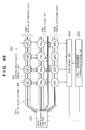
- Fig. 8 is a schematic circuit diagram of a sensor circuit (a drive circuit diagram of a CMOS sensor) disclosed in Japanese Patent Laid-Open No. 11-196332.
- This sensor circuit outputs a video signal to, e.g., the spatial filter circuit of the above-described image sensing signal processing circuit.
- photoelectric conversion elements are formed by photodiodes PD11 to PD22... with p-n junctions and transfer MOS transistors ST11 to ST22... connected to the cathodes of the photodiodes.
- a vertical selection circuit VSR sequentially sets outputs V1 to V8 to "H” to sequentially activate vertical selection lines HL1, HL2,....
- outputs H1 to H8 from a horizontal selection circuit HSR are sequentially set to "H” to turn on horizontal transfer switch MOS transistors HT1 to HT8.
- Image charges accumulated in the respective pixels are time-serially read out from vertical output lines HV1 to HV8 to an output line HOL and output through an amplifier AMP.
- a reset MOS transistor RES is turned on every time pixel charges are output, thereby resetting the output line HOL every time pixel charges are output.
- the photodiodes PD11 to PD22... the photodiodes PD11, PD12, PD21, PD22, PD31,... which are connected to the vertical output lines HV1 and HV2 are shielded from light on their cathode sides to extract dark charges.
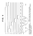
- Fig. 9 is a timing chart of the interlaced read of the solid-state image sensing apparatus.
- the pixels are read out every other pixel in the horizontal and vertical directions of photoelectric conversion elements in the effective signal range.
- the vertical selection circuit VSR sets the output V1 to "H” to set the vertical selection line HL1 to "H”. Subsequently, the outputs H1, H2, H3, H5, H7,... from the horizontal selection circuit HSR are sequentially set to "H”. With this operation, the horizontal transfer switch MOS transistors HT1, HT2, HT3, HT5, HT7,... are sequentially turned on. Image charges accumulated in the respective pixels are time-serially read out from vertical output lines HV1, HV2, HV3, HV5, HV7,... to the output line HOL and output through the amplifier AMP.
- the reset MOS transistor RES is turned on to reset the output line HOL every time the pixel charges are read out, thereby eliminating the influence of adjacent pixels.
- an output OUT from the amplifier AMP changes to "H" first because the reference signal output photoelectric conversion elements of the photodiodes PD11 and PD12 of the pixels are shielded from light. After that, a low-potential-side level is output in accordance with the charges of the first effective signal output photoelectric conversion elements of the photodiodes PD13, PD15, and PD17. In addition to such an interlaced read, a block read for reading an arbitrary range from an entire image is also done.
- the interval of the interfaced read can be arbitrarily changed.
- a prior art which applies a spatial filter after the above-described read is disclosed in Japanese Patent Laid-Open No. 2000-13694.
- time-serial image signals from a sensor must be spatially separated and individually input to corresponding feature extraction circuits.
- a sensor output must have one-to-one correspondence with the address of a feature extraction circuit on the array circuit.
- Image recognition or voice recognition schemes are roughly classified into a type for sequentially calculating and executing a recognition processing algorithm as computer software that is specialized to a specific recognition object and a type for executing recognition processing by a dedicated parallel image processor (e.g., an SIMD or MIMD machine).
- a dedicated parallel image processor e.g., an SIMD or MIMD machine.
- Typical examples of image recognition algorithms for calculating a feature vector associated with the similarity to a model to be recognized are a method using similarity calculation or higher-order correlation coefficient calculation, which is done by representing the model data of an object to be recognized as a template model and executing template matching with an input image (or its feature vector), and a method using hierarchical parallel processing (Japanese Patent No. 2741793).
- a scheme of determining the similarity to a local portion of a model to be detected is proposed in Japanese Patent Laid-Open No. 11-15945.
- matching processing between a local model and a local portion of an object is executed, and the degree of support for supporting the presence of the object at each local portion is obtained by integration processing based on the Dempster-Shafer theory or Fuzzy theory, thereby doing highly accurate detection.
- the arrangement of the pattern recognition apparatus disclosed in Japanese Patent Laid-Open No. 6-176158 cannot improve the memory efficiency or reduce the circuit scale.
- an arrangement for executing pattern recognition processing using hierarchical parallel processing circuits e.g., the arrangement disclosed in Japanese Patent No. 2741793
- a plurality of features are simultaneously parallelly detected at sampling points on input data.
- the number of elements in the lower layer increases depending on the size of an input image, resulting in an increase in circuit scale.
- an FPGA Field Programmable Gate Array
- An FPGA is formed by periodically arraying a plurality of relatively large circuit blocks and interconnection blocks on a chip.
- a number of “devices capable of programming" electrical connection or disconnection of the circuits are arranged in the circuit blocks and interconnection blocks.
- a user can design connections in and between the blocks in a field (site of use) by programming (defining) these devices.
- Cell library blocks having various kinds of logic circuits are arrayed in a matrix in a chip.
- Signal interconnections are formed horizontally and vertically between the cell library blocks.
- Switch elements are arranged at the interunits of the interconnections and between the interconnections.
- a desired logic function is described by an HDL (Hardware Description Language) using a support tool provided by an EDA vendor, and logic circuit data (the type of logic gate to be used and inter-terminal connection information) is obtained using a logic synthesizing tool.
- logic circuit data the type of logic gate to be used and inter-terminal connection information
- the logic operation data of a basic logic cell CLB and connection data between the basic logic cells CLB are obtained.
- interconnections to be used and the ON/OFF control data of a cross-point switch CSW are determined from the connection data, thereby building a whole logic circuit system.
- Such logic design can easily be done by the user, and its convenience is widely recognized.
- Arrangements disclosed in Japanese Patent Laid-Open Nos. 11-168185 and 2000-331113 are known as methods of reconfigurably connecting an analog processing element using an FPGA.
- an FPGA is formed on one surface of a stacked substrate
- an analog processing circuit is formed on the other surface
- input and output terminals and an interface circuit which connect the FPGA and analog processing circuit, are prepared.
- first and second analog signals are converted into PWM (Pulse Width Modulation) signals and input to an FPGA circuit, and logical operation of the two PWM signals is executed by the FPGA circuit, thereby allowingreconfiguration.
- PWM Pulse Width Modulation
- a hierarchical neural network disclosed in Japanese Patent No. 2679730 is related to the architecture of a hierarchical neural network that allows time-divisionally multiplexed use of single-layered hardware, and has as its object to allow equivalently making a multi-layered structure by time-divisionally using single-layered hardware.
- This prior art discloses a hierarchical neural network formed by connecting a plurality of neuron models to each other, comprising a single-layered unit assembling means for forming a single-layered unit assembly by installing a plurality of units of neuron models which allow to time-divisionally output a voltage through a nonlinear output function by generating a product of a time-divisionally multiplexed analog signal and external digital weight data and by time-divisionally adding the product through a capacitor to integrate the product, a feedback means for feeding back the output from the single-layered unit assembling means to the input unit of the same single-unit assembly, and a control means for executing control to time-divisionally multiplex analog signals from units, which are output from the single-layered unit assembling means, and to time-divisionally use the single-layered unit assembling means through the feedback means, wherein the single-layered unit assembling means is time-divisionally used to equivalently form a neural network having a hierarchical structure.
- programmable analog processing cells including a multiplexer, demultiplexer, control circuit, and analog processing element are parallelly arrayed through signal lines, thereby executing programmable analog processing.
- a so-called FPGA is based on a logic circuit. That is, only the connection state between logic blocks can be changed. Hence, only with the FPGA, analog parallel arithmetic processing of a neural circuit network or like cannot be implemented.
- each of the analog processing units has a control circuit, analog processing circuit element, signal branch circuit, and the like.
- the scale of the circuit component becomes very large, and therefore, the total circuit area inevitably increases.
- analog processing units each incorporating a multiplexer and demultiplexer are arrayed on a two-dimensional plane, it is difficult to realize an arbitrary connection structure and, more particularly, hierarchical connection.
- the present invention has been made in consideration of the above-described problems, and has as a concern to make it possible to efficiently sequentially extract a plurality of predetermined different geometrical features from time-serially input image data.
- Fig. 1 is a block diagram showing the overall arrangement of an image sensing signal processing circuit according to the first embodiment.
- a spatial filter circuit 1 time-serially executes predetermined spatial filter operations having different characteristics at points corresponding to the respective pixel positions, on the sensor, of a video signal input from a sensor circuit 3.
- the spatial filter circuit 1 has a function of time-serially extracting different geometrical image features for regions with a predetermined size around the respective points of a video signal.
- a control circuit 2 outputs a predetermined read control pulse signal to the sensor circuit 3 in accordance with a predetermined timing and also outputs a timing pulse signal synchronous with the read control pulse signal to the spatial filter circuit 1, thereby synchronously processing the output from the sensor circuit 3 and the spatial filter circuit 1, as will be described later. Detailed control of the spatial filter circuit 1 will be described later.
- a photoelectric conversion apparatus 10 in which photoelectric conversion elements are arrayed in a matrix, horizontal lines are sequentially activated by a vertical selection circuit VSR 11, and image signals from reference signal output photoelectric conversion elements and effective signal output photoelectric conversion elements are sequentially output through an amplifier AMP by a horizontal selection circuit HSR 12.
- the photoelectric conversion apparatus 10, vertical selection circuit VSR 11, and horizontal selection circuit HSR 12 correspond to a photoelectric conversion element array, vertical shift register 3v, and horizontal shift register 3h in Fig. 1, respectively.
- the output from the solid-state image sensing apparatus having the above arrangement is input to a reference voltage generator 14 during the output period of the reference signal output photoelectric conversion elements to generate a reference voltage.
- a reference voltage generator 14 When the number of reference signal output photoelectric conversion elements is 2, the average value of the outputs is defined as, e.g., a reference voltage.
- the output is input to a clamp circuit 13 and clamped to the reference voltage of the reference voltage generator 14.
- the reference voltage corresponding to dark charges in the same horizontal line of the photoelectric conversion apparatus is subtracted from the photocharge voltage of the effective signal output photoelectric conversion elements, thereby obtaining an image signal corresponding to the photocharges.
- the reference voltage of the reference voltage generator 14 is reset after one horizontal line is read, and newly generated by the reference signal output photoelectric conversion elements in reading another horizontal line.
- the difference between the reference voltage and the photocharge voltage of the effective signal output photoelectric conversion elements is calculated to output a substantial image signal.
- the output from the clamp circuit 13 is converted into a digital signal by an A/D converter 15 and subjected to spatial filter processing to be described below.
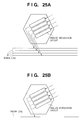
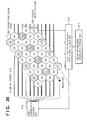
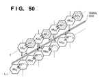
- Fig. 3 is a view showing a simplified arrangement of a spatial filter circuit element used in this embodiment.
- Fig. 3 illustrates outputs (h r (p ⁇ 1,q ⁇ 1), h i (p ⁇ 1,q ⁇ 1)) at adjacent pixel positions (p ⁇ 1,q ⁇ 1) closest to a pixel position (p,q).
- these circuit elements are two-dimensionally arrayed.
- h r (p,q) and h i (p,q) represent the real and imaginary parts of a filter output (to be described below) in correspondence with the pixel position (p,q) on the sensor, respectively. Input/output control of the spatial filter element circuit will be described later.
- the spatial filter used here is a Gabor filter or a so-called Gabor-type filter which outputs a signal approximate to a Gabor filter output.
- This filter has a spatial frequency selectivity in a predetermined direction, i.e., a direction selectivity (to have a sensitivity for edge components having a predetermined range of orientations in image) and a scale selectivity (to have a sensitivity for the size of a predetermined range in an image or the geometrical feature of a spatial frequency).
- Gabor wavelet transform is performed for an input image by multiple scale processing using a Gabor-type filter.
- a method and circuit for Gabor wavelet transform see, e.g., IEEE Trans. on Acoustics, Speech, and Signal Processing, vol. 36, pp. 1169-1179 (1988) and IEEE Trans. on Circuits and Systems-I: Fundamental Theory and Applications, vol. 45, pp. 121-132 (1998).
- the spatial filter used in this embodiment can control these selectivities by the characteristic of a circuit element (the conductance or the gain of an amplifier).
- Fig. 3 shows the arrangement of a circuit element which performs Gabor-type filtering operation for a local region around the given point (p,q) in an input image, which is based on reference 1 (B.E. Shi, "2D Focal Plane Steerable and Scalable Cortical Filters", Proc. of Seventh International Conference on Microelectronics for Neural, Fuzzy, and Bio-Inspired Systems, pp. 232-239, 1999).
- each trapezoidal element is typically a transconductance amplifier using five MOS transistors (an arrangement for changing a gain is disclosed in, e.g., Japanese Patent Laid-Open Nos. 7-235839 and 11-68477).
- Each resistive element is formed from a CMOS transmission gate (formed from, e.g., two CMOS transistors; reference 2: B.E. Shi, "Subthreshold Current Mode Design of Gabor-type CNN Image Filters", Proc. European Conference on Circuit Theory and Design, pp. 1163-1169, 1999).
- the label G of each resistive element indicates a conductance
- the label G of each transconductance amplifier indicates a gain.
- the filter circuit can operate each transistor either above or below a threshold value.
- a pixel signal is sent from the sensor circuit 3 driven by the read control pulse signal output from the control circuit 2 to a memory element C m in Fig. 3 at a predetermined timing.
- the memory element and a transconductance amplifier G S form the input unit of the spatial filter element circuit whose address (pixel position) is (p,q).
- a memory element and transconductance amplifier are present for each address (each filter element circuit).
- the filter output is read after image signal transfer to the input units (memory elements C m ) of the filter element circuits is complete.
- the pixel signal is temporarily held as a voltage signal by the memory element C m connected to the transconductance amplifier G S of the input unit.
- the output from the spatial filter circuit is read by a predetermined filter output read signal from the control circuit, the contents of the memory elements are rewritten.
- the data held by the memory element is converted from the voltage to a current by the transconductance amplifier G S and input as u(p,q).
- the direction selectivity and scale selectivity with a predetermined width centered on a spatial frequency (w x0 ,w y0 ) are obtained.
- w x0 atan(G 2x /G 1x )
- w y0 atan (G 2y /G 1y ).
- a filter characteristic & drive timing control signal for the spatial filter array circuit is output from the control circuit shown in Fig. 2 to the respective filter element circuits (Fig. 3) at once.
- the filter characteristic & drive timing control signal controls (updates) the respective filter characteristics of the filter element circuits at once.
- the above-described sensor circuit 3 executes interlaced read scanning for input image data at a predetermined interval and outputs image signal data.
- a control signal synchronized with the output timing of one frame from the spatial filter circuit array is output from the control circuit 2.
- image signal data at a corresponding address is read out from the sensor (photoelectric conversion element array) to the vertical and horizontal selection circuits in the sensor circuit 3 in accordance with a read control signal (sensor selection line signal in Fig. 1) synchronized with the control signal.
- a timing control signal (filter selection line signal in Fig. 1) is output, through a demultiplexer, to a predetermined spatial filter element circuit in the filter array circuit, which is specified by the sensor selection line signal (address in the input image). With this operation, image signal data at an address designated by a sensor selection line signal is transferred to a corresponding spatial filter element circuit.
- each spatial filter element circuit receives image data from the sensor after setting G 0 , G 1x , G 1y , G 2x , and G 2y in Fig. 3 (by the filter characteristic control signal from the control circuit 2) such that the spatial filter characteristic is represented by a set of parameter values to which the preset direction selectivity and scale selectivity belong.
- Gabor (type) filtering executed by each spatial filter will be described next.
- a Gabor function is obtained by modulating a sine wave having a predetermined direction component and spatial frequency by a Gaussian function (a non-Gaussian function for a Gabor-type filter). Its characteristic is set by an index m of scaling level and an index n of direction component (to be described below).
- a set of filter functions as a wavelet have a similar function shape and different main directions and magnitudes.
- the functional shape localizes both in the spatial frequency domain and in the real space domain, the conjoint uncertainty for the position and spatial frequency is minimum, and the function is localized most both in the real space and in the frequency space (J.G. Daugman, Uncertainty relation for resolution in space, spatial frequency, and orientation optimized by two-dimensional visual cortical filters, Journal of Optical Society of America A, vol. 2, pp. 1160-1169 (1985)).
- the direction selectivity parameter ⁇ n takes values of 0°, 30°, 60°, 90°, 120°, and 150° in six directions
- a is 2
- an the scale selectivity parameter m is given by an integer that takes values 1 to 3.
- these selectivities are realized by appropriately controlling the characteristic values (the conductance values and the gains of the conductance amplifiers) of the circuit element shown in Fig. 3.
- the characteristic parameters of a selected filter are given by m(t) about the scale selectivity and n(t) about the direction selectivity.
- the outputs of the spatial filter array of the circuit element shown in Fig. 3, i.e., h r (p,q) and h i (p,q) have a relationship given by W m(t)n(t) ⁇ h r (p,q) + jh i (p,q).
- Each spatial filter element circuit outputs a wavelet transform coefficient value obtained by product-sum input of distributed weight coefficients and image data. That is, for data of all frames from the sensor output, the outputs from the spatial filter circuit elements to which a predetermined filter characteristic is given are time-serially read out. In a similar way, filter outputs when a series of different filter characteristics are given are read out. Consequently, as the time-serial output of the entire spatial filter array (a set of values corresponding to W mn across the range of values that the indices m and n of equation (2) can take), the Gabor wavelet transform represented by equation (2) is executed.
- the time-serial output results for the respective filter characteristics updated in the following way are temporarily and individually stored in a plurality of temporary storage units (or in a single temporary storage means at once) as two-dimensional array data, and subsequent processing (e.g., image recognition processing) is executed.
- subsequent processing e.g., image recognition processing
- the subsequent processing module that receives the spatial filter output is a neural network circuit formed by parallelly and hierarchically connecting a plurality of arithmetic elements
- the above-described two-dimensional array data is (e.g., converted into a voltage signal) normally simultaneously output to the neural elements of the input layer at once.
- the control circuit 2 outputs control signals for corresponding resistance values and amplifier gains in the spatial filter circuit element.
- control circuit 2 outputs gate voltage control signals (V G1x , V G1y , V G0 ) for the transistors that form CMOS transmission gate circuits of the resistors and gain control signals (V G2x , V G2y ) for the transistors that form transconductance amplifiers as filter characteristic control signals such that the characteristics of the respective spatial filter circuit elements are updated at once.
- the control circuit 2 stores, in an internal storage unit 43, a table of data of sets of control signal values that give a set of conductance values and amplifier gain values (G 0 , G 1x , G 1y , G 2x , G 2y ) unique to the set ( m,n ) of the indices of the scale and direction selectivities of the Gabor-type filter.
- a gate control signal generator 42 When V con,(mn) is input from a direction/scale selection signal generator 41 as a control signal corresponding to each set of index, a gate control signal generator 42 outputs control signals V G1x , V G1y , V G2x , V G2y , and V G0 that give the following conductance values and amplifier gain values to the transistors of the resistors and amplifiers of the spatial filter circuit element shown in Fig. 3.
- G 1x(mn) ⁇ m 2 cos ( ⁇ m cos ⁇ n )
- G 2x,(mn) ⁇ m 2 sin( ⁇ m cos ⁇ n )
- G 1y,(mn) ⁇ m 2 cos( ⁇ m sin ⁇ n )
- G 2y,(mn) ⁇ m 2 sin( ⁇ m sin ⁇ n )
- Control signal lines to the resistors and amplifiers are wired to predetermined transistors of the circuit element shown in Fig. 3, though they are not illustrated for the illustrative convenience.
- the control circuit 2 outputs, to the horizontal selection circuit 3h and vertical selection circuit 3v in the sensor circuit 3, selection line signals for lines that should be sequentially set to "H" in the horizontal and vertical selection lines in synchronism with the output timing of the control signal from the above-described direction/scale selection signal generator 41.
- the pixel signal read out as a time-series signal is transferred to the input unit of the spatial filter circuit element (Fig. 3) selected by a demultiplexer circuit 5.
- the demultiplexer circuit 5 can have a normally used circuit arrangement (e.g., comprises a switch array and its activating circuit).
- the demultiplexer circuit 5 receives the preprocessed pixel signal and selection line signal and outputs a corresponding pixel signal to a Gabor-type spatial filter circuit element with corresponding address to the read pixel position in the input image, which is determined by the selection line signal.
- the read of the output from the Gabor-type spatial filter array circuit 1 will be described next.
- the read is done after the scale parameter m and direction component parameter n to be set by the direction/scale selection signal generator 41 in the control circuit 2 are updated, and all pixel signals to be input to the filter circuit elements are transferred.
- the transfer end timing of image data read out in correspondence with the parameters ( m,n ) of the Gabor-type filter to the filter circuit element is detected by inputting the last selection line signal.
- the spatial filter output is read out and stored in a temporary storage means as a plurality of two-dimensional array data (spatial filter array outputs for the same characteristic).
- these two-dimensional array data may be directly output to the subsequent processing module as time-serial data.
- the read of the spatial filter output is done after a predetermined delay time from the filter selection line signal output synchronized with the sensor selection line signal from the control circuit 2. For this reason, the spatial filter output can always be extracted while holding a predetermined time correspondence with the image signal output from the sensor.
- the readout time-serial filter outputs are branched and output by a demultiplexer circuit to the elements of the input stage of the apparatus.
- the input unit of each element has a sample-and-hold circuit or temporary storage memory element for holding the value of the input data.
- the time-serial filter outputs may be written in a predetermined block memory element as two-dimensional array data and then output to the input element array of the parallel arithmetic apparatus at once.
- address control or transfer control of the sensor circuit 3 is executed on the basis of the timing control of the spatial filter circuit 1.
- the same control as described above may be executed on the basis of the output timing of an intermediate processing circuit other than the above-described spatial filter, e.g., the pattern recognition circuit.
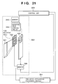
- An image sensing apparatus shown in Fig. 5 has an imaging optical system 92 including a photographing lens and zoom photographing drive control mechanism, a CMOS image sensor 93, an image sensing parameter measurement unit 94, an image sensing signal processing circuit 95 which performs spatial filter operation of this embodiment, a storage unit 96, a control signal generation unit 97 for generating a control signal to control the image sensing conditions, a display 98 that also serves as a viewfinder such as an EVF, an electronic flash 99, a recording medium 910, and an object recognition unit 911.
- the object recognition unit 911 has a function of detecting a pattern of a specific category from an image using a Gabor-type wavelet transform output from the image sensing signal processing circuit 95.
- This image sensing apparatus 9 detects the facial image (detects the position and size) of a person, which is registered in advance, from, e.g., a photographed video image using the object recognition unit 911.
- the position and size information of the person are input to the control signal generation unit 97.
- the control signal generation unit 97 generates a control signal for optimizing focus control, exposure condition control, and white balance control for that person on the basis of the output from the image sensing parameter measurement unit 94.
- the object detection (recognition) function can be realized with a small circuit scale at low power consumption and high speed (in real time). On the basis of the result, detection of a person and optimum control (AF, AE, and the like) of photography based on it can be executed.
- This embodiment is applied when the sensor circuit 3, control circuit 2, preprocessing circuit 4, and spatial filter circuit 1 shown in Fig. 1 are formed on separate semiconductor chips or on a single semiconductor chip.
- circuits shown in Fig. 1 are formed on a single semiconductor chip by a CMOS process or the like, this embodiment exhibits a better effect.
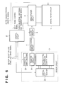
- Fig. 6 is a block diagram showing the arrangement of main part of the second embodiment. According to this arrangement, the memory element C m at the input unit of the spatial filter circuit element shown in Fig. 3 is unnecessary. Of a sensor circuit output, a necessary portion corresponding to a predetermined spatial filter circuit element to be time-serially accessed is temporarily recorded in a block memory 6. Then, pixel data in the block memory 6 are read out at once (time-serially in the case of the first embodiment where the memory element C m is used in the circuit shown in Fig. 3) as voltage signals, and the above-descried spatial filter processing is performed.
- a control circuit 2 sends, of spatial filter characteristic parameters ( m,n ), a scale control signal corresponding to the scale parameter m to a sensor circuit 3 side together with an address selection signal.
- the horizontal and vertical selection circuits (3h and 3v) in the sensor circuit 3 make the block memory 6 store image data of a local region (local region sampled by an interlace read) about each sampling pixel for a predetermined region size corresponding to the scale control signal. With this operation, the load on the control circuit 2 which outputs the read timing control signal to the sensor circuit 3 can be reduced.
- the block memory 6 functions as a temporary storage element.
- image data in the local region (its size depends on the scale parameter) around each sampling position is sent to each spatial filter circuit element corresponding to the position of the sampling point.
- the image data stored in the block memory 6 is output in the following manner. Every time the sampling position of the interlaced read is updated by the control signal from the control circuit 2, image signal data (that has undergone preprocessing) in the block memory 6, which corresponds to the sampling position, is transferred to the spatial filter array circuit. After that the image signal from the sensor at that position (address) is input and that the image data at a corresponding address on the block memory 6 is rewritten, the image data in the block memory is updated as image data overlapped in a predetermined range.
- the image data are time-serially output as image signals from the block memory 6 to the spatial filter circuit elements.
- the output read from the spatial filter circuit 1 and the like are the same as in the first embodiment.
- the sensor circuit 3, control circuit 2, preprocessing circuit 4, and spatial filter circuit 1 shown in Fig. 6 may be formed on separate semiconductor chips or on a single semiconductor chip. However, when the circuits are formed on a single semiconductor chip, this embodiment exhibits a better effect.
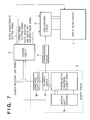
- Fig. 7 shows the arrangement of main part of the third embodiment.
- Timing control characteristic of a sensor circuit 3, i.e., the modulation timing control on a spatial filter circuit 1 side is done using a read control signal used in a normal CMOS sensor.
- interlaced read control as in the first embodiment is done.
- a control circuit 2 receives selection line signals in the sensor read mode to obtain the address information of an image signal and executes transfer control of the image signal to a spatial filter circuit element at a corresponding position.
- characteristic control signals for circuit elements (resistors and transconductance amplifiers) shown in Fig. 3 are sent in correspondence with the characteristic parameters ( m,n ) of Gabor-type wavelet transform shown in the first embodiment.
- the signals are updated after a series of readout operations from the sensor are ended. For example, the signals are updated every time the interlaced readout to be executed for the input image is ended. After the updating, the (interlaced) readout scanning is performed by the sensor circuit 3.
- a pixel signal is temporarily held by a memory element C m connected to a transconductance amplifier G S at the input unit as a voltage signal, as in the first embodiment.
- the output from the spatial filter circuit 1 is read out, the contents of the memory element are rewritten.
- the remaining operations and arrangements are the same as in the first embodiment.
- the sensor circuit 3, control circuit 2, preprocessing circuit 4, and spatial filter circuit 1 shown in Fig. 7 are formed on separate semiconductor chips or on a single semiconductor chip. However, when the circuits are formed on a single semiconductor chip, this embodiment exhibits a better effect.
- a plurality of spatial filter arithmetic operations for a plurality of different spatial filter characteristics are executed not parallelly by a plurality of spatial filter circuits but time-serially by a single spatial filter.
- the chip In a structure in which the sensor circuit 3 and spatial filter circuit 1 are formed on a single semiconductor chip, if any one of the sensor circuit 3 and spatial filter circuit 1 has a defect, the chip cannot be used. Hence, the yield decreases. If a plurality of spatial filter circuits are formed, the chip area becomes large, and the yield becomes very low. However, as in the above-described first to third embodiments, when processing operations are executed time-serially by one spatial filter circuit 1, the chip area decreases, and the yield improves.
- any decrease in yield due to formation of a plurality of spatial filter circuits on a single semiconductor chip can be prevented.
- advantages of reduction of the area, power consumption, and cost can be obtained by forming the circuits on a single semiconductor chip.
- a plurality of spatial filter arithmetic operations are time-serially executed in correspondence with a plurality of different spatial filter characteristics.
- a plurality of predetermined different geometrical features can be efficiently and sequentially extracted from time-serially input image data using a single circuit.
- the temporally modulated spatial filter output can be synchronized with the sensor output timing, different spatial filter processing operations can be efficiently and stably executed for a sensed image.
- a sensor region including a pixel array having a photoelectric conversion characteristic and a circuit for reading image data from the pixel array, and a single spatial filter circuit for time-serially executing a plurality of spatial filter arithmetic operations for single image data read out from the sensor region in correspondence with a plurality of different spatial filter characteristics are formed on a single semiconductor chip.
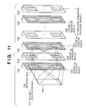
- Fig. 10 is a block diagram showing the overall arrangement of a pattern recognition apparatus according to this embodiment, which is constituted by a block-shaped local region scanning unit 301 in input data, an image input unit 302, a local region recognition processing module 303, a time-serial integration processing module 304, a determination unit 305, and a control unit 306 for controlling their operations.
- a pattern recognition apparatus which is constituted by a block-shaped local region scanning unit 301 in input data, an image input unit 302, a local region recognition processing module 303, a time-serial integration processing module 304, a determination unit 305, and a control unit 306 for controlling their operations.
- the outline of the function of each component will be described next.
- the scanning unit 301 sets a local region (block-shaped region) having a predetermined size and rectangular shape (or any other shape) set by the control unit 306 at each sampling position in input data from the image input unit 302 while updating the sampling position on the basis of a control signal from the control unit 306.
- a local region after being updated by scanning preferably overlaps that before the updating in a predetermined range such that the detection accuracy is prevented from degrading when a feature is present near the boundary.
- the scanning unit 301 outputs a read control signal to the image input unit 302 (a sensor such as a CMOS sensor) to receive the signal of a block-shaped local region from the sensor.
- a known method e.g., a method disclosed in Japanese Patent Laid-Open Nos. 11-196332 by the present applicant
- a CCD is used as a sensor, an image is temporarily stored in a frame memory or the like and scanned while extracting a block-shaped region.
- the local region recognition processing module 303 is formed from hierarchical neural network circuits for detecting lower- to higher-order geometrical features.
- the local region recognition processing module 303 receives the data of the set block-shaped region and outputs to the serial integration processing module 304 a signal representing whether a medium- or higher-order pattern of a predetermined category is present in the local region.
- the time-serial integration processing module 304 receives position information from the scanning unit 301, integrates, on the basis of that information, the outputs from the local region recognition processing module 303 for the respective block-shaped regions set at a plurality of positions by a method to be described later, and outputs information about the presence/absence of a predetermined pattern. Upon receiving a detection signal (position and category information) of a higher-order pattern (recognition object) from the local region recognition processing module 303, the time-serial integration processing module 304 directly outputs the detected information to the determination unit 305.
- the determination unit 305 When a predetermined pattern is detected for the output from the time-serial integration processing module 304 using determination parameters supplied from the control unit 306, the determination unit 305 outputs information representing a specific category whose pattern is present in the input data, and a specific position of the pattern.
- the local region recognition processing module 303 will be described next in detail with reference to Fig. 11.
- the processing module 303 mainly concerns recognition (detection) of objects or geometrical features in local regions in input data.
- Its basic structure is a so-called convolutional network structure (Y. Le Cun and Y. Bengio, "Convolutional Networks for Images Speech, and Time Series" in Handbook of Brain Theory and Neural Networks (M. Arbib, Ed.), MIT Press, pp. 255-258, 1995).
- This structure is different from the prior art in that inter-layer connection may locally form mutual connection (to be described later).
- the final output corresponds to a recognition result, i.e., the category of a recognized object and its position on the input data.
- a data input layer 101 inputs local region data from a CMOS sensor or a photoelectric conversion element such as a CCD element under the instruction of the scanning unit 301.
- the data input layer 101 may input higher-order data obtained from the result of an analysis (e.g., principal component analysis, vector quantization, or the like) of a predetermined data analysis unit.
- the first feature detection layer (1,0) detects a local lower-order feature (it may include not only a geometrical feature but also a color component feature) from an image pattern input from the data input layer 101 for each local region around each position in the entire frame (or for each local region around each predetermined sampling point in the entire frame) by multiple resolution processing using Gabor wavelet transform and the like by a plurality of feature categories at a portion at a plurality of scale levels or resolutions.
- a local lower-order feature it may include not only a geometrical feature but also a color component feature
- the feature detection layer (1,0) is formed from neuron elements, each of which has a receptive field structure corresponding to the type of feature (e.g., the gradient of line segment as a geometrical structure in the case of extracting a line segment in a predetermined direction) and generates a pulse sequence corresponding to the degree.
- the type of feature e.g., the gradient of line segment as a geometrical structure in the case of extracting a line segment in a predetermined direction
- a feature detection layer 102 (1,k) forms a process channel at a plurality of resolutions (scale levels) as a whole, as described in detail in USSN 09/878,269 and European Patent Application No. 01305231 by the present applicant (k ⁇ 0).
- a case wherein Gabor wavelet transform is executed by the feature detection layer 102 (1,0) will be exemplified.
- a set of feature detection cells having Gabor filter kernels with the same scale level and different direction selectivities as receptive field structure form a process channel in the feature detection layer 102 (1,0).
- feature detection cells the feature detection cells detect higher-order features
- feature detection cells for receiving the outputs for the feature detection cells belong to the same channels as those process channels.
- feature detection cells for receiving the outputs for a plurality of feature integration cells forming identical channels in a layer 103 (2,k-1) are designed to belong to the channels.
- Gabor wavelet has a shape obtained by modulating a sine wave having a predetermined direction component and spatial frequency by a Gaussian function.
- a set of filters as a wavelet have a similar function shape and different main directions andsizes.
- the functional shape is localized in the spatial frequency domain and in the real space domain, the conjoint uncertainty for the position and spatial frequency is minimum, and the function is the most localized both in the real space and in the frequency space (J.G. Daugman, Uncertainty relation for resolution in space, spatial frequency, and orientation optimized by two-dimensional visual cortical filters, Journal of Optical Society of America A, vol. 2, pp. 1160-1169 (1985)).
- the respective process channels progress processing holding the respective scale level (or resolution) assigned to them and detect and recognize lower- to higher-order features by hierarchical parallel processing.
- a feature integration layer 103 (2,0) is formed from a neuron element which has a predetermined receptive field structure (a receptive field means the connection range with the output element of the immediately preceding layer, and a receptive field structure means the distribution of connection weight values) and generates a pulse sequence.
- the feature integration layer 103 (2,0) integrates (by means of arithmetic processing such as local averaging or sub-sampling by maximum output detection) a plurality of neuron element outputs in the same receptive field from the feature detection layer 102 (1,0).
- the receptive fields of neurons in a single feature detection layer have a common structure.
- Each of the subsequent feature detection layers 102 (1,1), (1,2),..., (1,M) and feature integration layers 103 (2,1), (2,2),..., (2,M) has a predetermined receptive field structure.
- the former ((1,1),%) detects a plurality of different features in each feature detection module.
- Each of the latter ((2,1),...) integrates detection results about some feature from the preceding feature detection layer.
- the former feature detection layer is connected (wired) to receive the outputs from neuron elements in the preceding feature integration layer belonging to the same channel.
- outputs from a local region (local receptive field of the feature integration layer neuron) from feature detection cells of the same feature category are undergoes averaging or else.
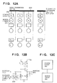
- Figs. 12A to 12C are views showing the arrangements of a synapse circuit and neuron element.
- the structure for connecting elements 201 in-between neurons in the respective layers includes a signal transmission unit 203 (interconnection or delay line), corresponding to the axon or dendrite of a neuron, and synapse circuits 202, as shown in Fig. 12A.
- Fig. 12A shows the arrangement of a connection section related to the outputs (inputs when viewed from the cell) of neurons (n i ) of a feature integration (detection) cell that forms a receptive field with respect to a given feature detection (integration) cell.
- a portion serving as a signal transmission unit indicated by a bold line forms a common bus line.
- Pulse signals from a plurality of neurons are time-serially arranged and transmitted on the signal transmission line.
- the same arrangement is employed to receive an input from a cell at an output designation.
- input and output signals may be time-divisionally processed in the same arrangement.
- the same arrangement as in Fig. 3 may be prepared for each of the input side (dendrite side) and output side (axon side) to process the signals.
- So-called excitatory connection amplifies a pulse signal in the synapse circuit 202.
- inhibitory connection attenuates the signal.
- amplification and attenuation can be realized by any one of amplitude modulation, pulse width modulation, phase modulation, and frequency modulation of the pulse signal.
- each of the synapse circuit 202 is mainly used as a pulse phase modulation element. Amplification of a signal is converted into a substantial advance of the pulse arrival time as an amount unique to a feature. Attenuation is converted into a substantial delay.
- synapse connection gives an arrival position (phase) on a time axis unique to each feature at a neuron as an output destination (as will be described later).
- Excitatory connection qualitatively gives an advance in phase of an arrival pulse with respect to a reference phase, and inhibitory connection gives a delay.
- each neuron element n j outputs a pulse signal (spike train) and uses a so-called integrate-and-fire type neuron element (as will be described later).
- a synapse circuit and neuron element may be put into a circuit block.
- Each neuron element is an extention of a so-called integrate-and-fire neuron model.
- Each neuron element is the same as a so-called integrate-and-fire neuron in that the element fires and outputs a pulse signal when a result obtained linearly and time-spatially adding input signals (pulse sequence corresponding to an action potential) exceeds a threshold value.
- Fig. 12B shows the basic arrangement representing the operation principle of a pulse generation circuit (CMOS circuit) serving as a neuron element. It is an extended version of a known circuit (IEEE Trans. on Neural Networks Vol. 10, p. 540). As inputs, excitatory and inhibitory inputs are received.
- CMOS circuit pulse generation circuit
- IEEE Trans. on Neural Networks Vol. 10, p. 540 As inputs, excitatory and inhibitory inputs are received.
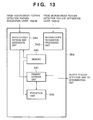
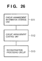
- the time-serial integration processing module 304 comprises a higher-order pattern map generation unit 341 for generating a map of the detection level (the type of a feature as needed) and position of higher-order patterns, a medium-order integration processing unit 342 for outputting the predicted position of the medium-order pattern to be detected, and outputting a higher-order pattern category that matches best, a memory 343 for storing the higher-order pattern category (e.g., the data of template data) and a temporal storage unit 344 for storing the predicted position (to be described later).
- a higher-order pattern map generation unit 341 for generating a map of the detection level (the type of a feature as needed) and position of higher-order patterns
- a medium-order integration processing unit 342 for outputting the predicted position of the medium-order pattern to be detected, and outputting a higher-order pattern category that matches best
- a memory 343 for storing the higher-order pattern category (e.g., the data of template data)
- Pieces of information related to the presence/absence and presence positions of a higher-order pattern (e.g., a facial pattern to be finally recognized) in a local region and medium-order patterns (e.g., patterns corresponding to the eye, nose, or mouth in a face) having intermediate complexity as a component of the higher-order pattern are output from the local region recognition processing module 303 to the time-serial integration processing module 304.
- medium-order pattern detection information may be integrated by time-serial processing (to be described later) in the medium-order integration processing unit 342 and used for the detection of a higher-order pattern having a larger size.
- neuron outputs from the feature integration layer 103 (2,m) related to medium-order feature detection and the final layer 103 (2,M) that gives higher-order feature (object) detection information in the local region recognition processing module 303 are supplied to the time-serial integration processing module 304 through a predetermined bus line.
- the neuron output from the feature integration layer 103 (2,m) is supplied to both of the next feature detection layer 102 (1,m+1) and a bus line serving as an output to the time-serial integration processing module 304.
- signal transmission between neurons by pulse signals can be executed by so-called AER (Address Event Representation) (Lazzaro et al. Silicon Auditory Processors as Computer Peripherals, in Tourestzky, D. (ed), Advances in Neural Information Processing Systems 5. San Mateo, CA: Morgan Kaufmann Publishers, 1993) or the like.
- a prediction unit 346 in the time-serial integration processing module 304 selects one of higher-order pattern candidates that can be constructed by the medium-order pattern.
- the category and position (configuration) information of another medium-order pattern to be detected, which constructs the candidate pattern, are predicted by the method to be described later.
- the medium-order integration processing unit 342 outputs to the determination unit 305 information corresponding to the detection probability (or the confidence coefficient of detection) of the pattern of the category to be detected at an output level depending on whether the pattern of the predicted category is detected at a corresponding position (when the predicted pattern is detected at the predicted position, the output level becomes high).
- the control unit 306 receives the position information of the predicted medium-order pattern from the time-serial integration processing module 304 and outputs sampling position update control information for the scanning unit 301 such that data in a local region around that position of that feature is provided next. Details of this process will be described later with reference to Fig. 14.
- the local region recognition processing module 303 detects a higher-order pattern with an output level equal to or more than a predetermined threshold value in the local region, information (corresponding to the detection probability or the confidence coefficient of detection) related to the category and the position information of the detected object in the local region are output to the time-serial integration processing module 304.
- the control unit 306 obtains the position information of the detected pattern from the scanning unit 301 and outputs the position information to the determination unit 305.
- the output from the neuron that gives the maximum value is supplied to the time-serial integration processing module 304, giving the category and position information of the detected object.
- both the higher-order pattern and medium-order pattern are detected in the same local region by the local region recognition processing module 303 (the detection levels of both patterns are equal to or more than a predetermined threshold value).
- a neuron output that gives the above-described maximum value output is supplied to the higher-order pattern map generation unit 341 of the time-serial integration processing module 304.
- the neuron output of the above-described feature integration layer 103 (2,m) is supplied to the medium-order integration processing unit 342 through the bus line.
- the time-serial integration processing module 304 the above-described processing is executed for each of the higher-order pattern and medium-order pattern.
- the medium-order integration processing unit 342 in the time-serial integration processing module 304 will be described next.
- the medium-order integration processing unit 342 is a signal processing circuit (or so-called middleware) for outputting the predicted category of some undetected medium-order patterns about a higher-order pattern that can be comprised of detected medium-order patterns, and the predicted position near the position of the detected medium-order pattern.
- the medium-order integration processing unit 342 obtains the class (the pattern of the other eye, nose, or mouth), i.e., the predicted category of another undetected medium-order pattern, and its predicted position.
- the circuit (prediction unit 346) for executing the above-described prediction processing is formed as a kind of logic circuit that outputs a result by looking up combinational, list structured data described in advance in a list or dictionary format and supplementary data (relative position vectors of medium-order patterns as candidates) without executing any probability processing and other complex processes with large computational load.
- the list structure data is given by a list structure in which medium-order patterns of a higher-order pattern are linked with each other. Supplementary data is represented using relative position vectors for the distance and directions between medium-order patterns.
- the predicted position can be dependent on the class of the detected medium-order pattern and the type of the above-described process channel to which the maximum value output neuron of the feature integration layer 103 (2,m) in the local region recognition processing module 303 belongs. That is, in this embodiment, the type of process channel reflects the difference in size of an object to be detected or a feature. The position (predicted position) of some undetected medium-order pattern also changes depending on the size.
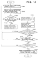
- step S101 the category information of a higher-order pattern that has a medium-order pattern category detected by the local region recognition processing module 303 as a component is read out from the memory 343 in the time-serial integration processing module 304.
- step S102 the category and predicted position of a medium-order pattern that will be detected near the detected medium-order pattern with a high likelihood are obtained for each higher-order pattern and stored in the temporal storage unit 344.
- step S103 it is determined whether a plurality of undetected medium-order patterns may exist near the predicted positions. If YES in step S103, a medium-order pattern close to the default scanning direction (e.g., rightward from the upper left corner to the lower right corner) is selected (S104).
- S104 a medium-order pattern close to the default scanning direction (e.g., rightward from the upper left corner to the lower right corner) is selected (S104).
- step S105 the predicted position output selected by the medium-order integration processing unit 342 is input to the control unit 306 and used for updating the control of the scanning position.
- the predicted position information is converted into updated position data of a local region to be set by the scanning unit 301 and supplied to the scanning unit 301.
- step S106 the local region recognition processing module 303 supplies, to the medium-order integration processing unit 342, the output from the feature integration layer 103 (2,m) related to the medium-order pattern as a processing result about the predicted category (medium-order pattern level) at the predicted position for a higher-order pattern candidate that is compatible with the detected medium-order pattern (in a predetermined order).
- the medium-order integration processing unit 342 in the time-serial integration processing module 304 receives a recognition processing result for the local region data from the local region recognition processing module 303 in accordance with an instruction from the scanning unit 301 (as in S104) and determines the degree of compatibility with the category of the already detected medium-order pattern in the following way (S107). If it is determined that the pattern is compatible with, the category information of a corresponding higher-order pattern and its detection level (corresponding to the presence probability or the confidence coefficient of detection) are output to the determination unit 305 (S110).
- the above-described prediction and verification at the medium-order pattern level are repeated as long as an undetected medium-order pattern is present and as long as undetected higher-order pattern is present (S108 and S109).
- Compatibility determination between medium-order patterns based on the category of a higher-order pattern (processing in S107) will be described next.
- the correspondence between category and spatial arrangement information in the remaining medium-order patterns that goes with these categories is stored in a memory in advance as a table, thereby realizing so-called true-false determination processing by a simple logic circuit.
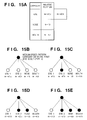
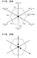
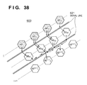
- Fig. 15A shows data representing the correspondence.
- the correspondence data is given in a table format.
- the category of the higher-order pattern is "face”
- the category of a medium-order pattern that is detected first is “eye”
- its size is given by a process channel number k (scale level k) of the feature integration layer 103 (2,m) related to the medium-order pattern.
- the categories and position information of remaining medium-order patterns that goes with the above patterns are given by "nose” and r c-n,k , "mouth” and r c-m,k , "eye” and r e-c1,k and r e-c2,k .
- r is the relative position vector with respect to the already detected medium-order pattern.
- the "eye” that corresponds to the medium-order pattern to be detected is determined by judging whether a pattern corresponding to an "eye” that should exist in the direction of the predicted position is present (whether a right or left eye is estimated at this time). As is apparent, when a plurality of medium-order patterns such as "eye” and "nose” are already detected, the relative position vector of the remaining medium-order pattern "mouth” is uniquely determined.
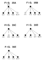
- Fig. 15B shows medium-order patterns (eye, nose, and mouth) represented by a tree structure when a medium-order pattern (eye) is detected first for a given higher-order pattern category (face), and the detection process.
- Each node is either in an undetected state ( ⁇ ) or detected state ( ⁇ ).
- Eye 1 and eye 2 represent left and right eyes, respectively.
- the detection state transits from Fig. 15B to Fig. 15E. In this case, eye 2 is detected at the predicted position as one of the eyes.
- the determination unit 305 comprises a threshold value processing unit 351 and detected pattern map information generation unit 352.
- the threshold value processing unit 351 executes threshold value processing of a higher-order pattern detection level signal from the time-serial integration processing module 304. To control the threshold value depending on input data (object to be detected), the threshold value information is input from the control unit 306.
- the detected pattern map information generation unit 352 stores the category and position information of the higher-order pattern in a memory 307 for holding pattern map information detected for the entire input data. Alternatively, the detected pattern map information generation unit 352 outputs the information to a predetermined display unit.
- the recognition processing circuit can execute processing for only a partial region in input data and detection based on both medium-order and higher-order patterns. For this reason, the circuit scale can be largely reduced, and the efficiency of recognition processing can be made high as compared to an arrangement for simultaneously and parallelly detecting a plurality of features individually at given sampling positions on input data.
- the above-described pattern recognition apparatus can be mounted in an image input apparatus such as a camera or an image output apparatus such as a printer or display.
- an image input apparatus such as a camera or an image output apparatus such as a printer or display.
- predetermined operations e.g., for the image input apparatus, processes such as focusing, exposure correction, zooming, and color correction for a specific object can be executed.
- processes such as optimum color correction for a specific object can be automatically executed.
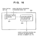
- An image sensing apparatus shown in Fig. 5 has an imaging optical system 92 including a photographing lens and zoom photographing drive control mechanism, a CCD or CMOS image sensor 93, an image sensing parameter measurement unit 94, an image sensing signal processing circuit 95, a storage unit 96, a control signal generation unit 97 for generating a control signal to control the image sensing operations or image sensing conditions, a display 98 that also serves as a viewfinder such as an EVF, an electronic flash 99, and a recording medium 910.
- This apparatus also has an object detection (recognition) apparatus 911 as the above-described pattern recognition apparatus for executing time-divisional multiplexed processing.
- the object detection (recognition) unit 911 detects the facial image (detects the position and size) of a person, which is registered in advance, from, e.g., a photographed video image.
- the position and size information of the person are input from the object detection (recognition) apparatus 911 to the control signal generation unit 97.
- the control signal generation unit 97 generates a control signal for optimizing focus control, exposure condition control, and white balance control for that person on the basis of the output from the image sensing parameter measurement unit 94.
- sampling point position control does not depend on the intermediate output result of a local region recognition processing module 303.
- the local region recognition processing module 303 detects a medium-order or higher-order pattern, as in the above embodiment.
- the arrangement as a pattern recognition apparatus is the same as in the fourth embodiment.
- a pattern detected as a higher-order pattern has a size equal to or smaller than the block size.
- the local region recognition processing module 303 has process channels unique to a plurality of sizes to be detected, as in the fourth embodiment.
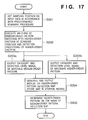
- Fig. 17 shows the processing chart of this embodiment.
- step S201 a sampling point position is set on input data in accordance with a predetermined scanning procedure.
- step S202 medium-order patterns compatible with a higher-order pattern at the sampling point position is detected, and then the higher-order pattern is detected.
- a time-serial integration processing module 304 stores, in a temporal storage unit 344, the category, detection level, and position information of the pattern as detected pattern distribution (map) information.
- the stored medium-order pattern data forms a higher-order pattern having a size (larger than the block size) that is not detected in the local region with the given size.
- the determination unit 305 determines the presence/absence of an object to be recognized (higher-order pattern), i.e., the presence/absence of a higher-order pattern (object to be detected) (when the higher-order pattern is present, its position and category information) around the position at which the medium-order pattern is detected (since the block size is limited at that position, no higher-order pattern comprised of the medium-order pattern is detected) by looking up the temporal storage unit 344 in the time-serial integration processing module 304 (S205).
- high-order pattern i.e., the presence/absence of a higher-order pattern (object to be detected)
- Processing executed in step S205 is no simple threshold value processing, unlike the fourth embodiment. As shown in Fig. 18, processing executed in step S205 is almost the same as the flow chart in the time-serial integration processing module 304 in the fourth embodiment. This processing is performed in the following way while scanning on the medium-order pattern detection map information that is temporarily stored in the temproal storage unit 344.
- step S211 the category of a higher-order pattern is input and selected.
- step S212 in scanning on the detection map, the predicted position to which scanning should jump next and feature category are obtained. Processing that is executed when a plurality of medium-order patterns that may go with the higher-order pattern exist in the neighborhood (steps S215 and S216) is the same as in the processing by the time-serial integration processing module 304 in steps S105 and S106 of Fig. 14 in the fourth embodiment.
- step S217 compatibility with the higher-order pattern at the predicted position is determined by simple logic determination processing (step S217). Processing in steps S211 to S217 is repeated until the numbers of undetected medium- and higher-order patterns become zero (steps S218 and S219). The map information of the detected higher-order pattern is finally output (S210).
- recognition and integration processes are executed by a local region recognition processing module 303, time-serial integration processing module 304, and determination unit 305 while the size of a block-shaped region set by a scanning unit 301 is controlled by a block setting unit 302.
- the local region recognition processing module 303 parallelly forms a plurality of process channels corresponding to the difference in scale level, as in the fourth embodiment.
- update control of the block size the following two methods can be used.
- the block size is updated by a control unit 306 at each scanning position, and an output from the local region recognition processing module 303 is obtained every time.
- a series of recognition and integration processes are executed for input data in accordance with a predetermined size and predetermined scanning procedure, and then, the block size is changed, and the same recognition and integration processes are repeated.
- the local region recognition processing module 303 only detects a higher-order pattern.
- the output to the time-serial integration processing module 304 is output from only the uppermost feature integration (or detection)layer.
- the processing contents in the local region recognition processing module 303 are the same as in the above-described embodiment.
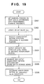
- Fig. 19 shows the main processing chart of this embodiment.
- step S301 the sampling point position on input data is set in accordance with a predetermined scanning procedure.
- step S302 the block size is set or updated in accordance with the predetermined procedure (as described above).
- step S303 higher-order pattern detection processing in the local region is executed by the local region recognition processing module 303. After that, in step S304, the detection level of a pattern that goes with a higher-order pattern category prepared in advance is output.
- step S305 the time-serial integration processing module 304 receives the detection level and category of the higher-order pattern from the local region recognition processing module 303, receives corresponding scanning position information from the control unit, and outputs a higher-order pattern detection map (stores the map in the storage unit).
- the control unit 306 executes threshold value processing (S306) and outputs information representing the position of the higher-order pattern (object to be detected) in the input data.
- the difference in block-shaped local region size in the scanning process corresponds to the difference in process channel of the local region recognition processing module 303 described in the fourth embodiment.
- a higher-order pattern having a different size is detected at each scanning position.
- the circuit scale and power consumption of the respective processing modules can be minimized.
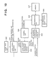
- Fig. 20 is a view showing the arrangement of main part of the seventh embodiment.
- the number of types (categories or sizes) of features to be detected in each feature detection layer at given time is one.
- the local region recognition processing module 303 hierarchically holds intermediate processing results about pattern detection of a category which is time-serially changed in memories 398 0 , 398 1 ,..., 398 M .
- the detection results in feature integration layers are read out from the memories 398 0 , 398 1 ,..., 398 M and integrated by a time-serial integration processing module 304.
- feature detection layers 102 and feature integration layers 103 which are alternately cascaded hierarchically detects lower- to higher-order patterns, as in the above embodiment.
- the outputs from the respective feature detection layers 102 undergo the same sub-sampling processing as in the above embodiment in the subsequent feature integration layers 103 and are temporarily stored in the memories 398 0 , 398 1 ,..., 398 M accompanying the feature integration layers (103) at an address that changes depending on the feature type.
- the feature detection layer 102 updates the synaptic weight distribution (local receptive field structure), as will be described below, and also receives the detection result for each feature type from the memory 398.
- the local receptive field structure of the feature detection layer 102 is held as digital data in a memory 340 such as an SRAM for each feature type to be input, read out from the memory, and updated.
- the local receptive field structure is given by a dynamically reconfigurable FPGA or FPAA (Field Programmable Analog Array) and a receptive field control circuit 345 of an accompanying synapse element circuit.
- the receptive field structure of the neuron of the feature detection layer 102 (layer for detecting a medium-order feature) that was detecting a pattern corresponding to an eye at certain time is updated in a predetermined order in accordance with signals from the control unit 306 and receptive field control circuit 345 such that a pattern corresponding to the nose or mouth is detected at another time.
- multiplex processing is executed such that different feature detection (recognition) processes are time-serially executed by the circuit of one local region recognition processing module 303.
- the circuit scale can be largely reduced, as compared to a circuit arrangement for simultaneously detecting a plurality of features in parallel individually at sampling positions on input data.
- the structure of the receptive field temporally controlled is given by a dynamically reconfigurable FPGA (FPAA), an SRAM (not shown) for storing a configuration bit (to be referred to as a CB hereinafter) as the configuration data of the FPGA (FPAA), the memory 340 for providing the CB to the SRAM, and the receptive field control circuit 345.
- the CB is data that reflects the receptive field of each neuron.
- a memory and control circuit for updating the CB for each neuron are generally necessary.
- one set of a CB, memory 340, and receptive field control circuit 345 suffices for one feature category to be detected.
- the memory 340 and receptive field control circuit 345 which give the receptive field structure, can be shared to time-serially supply a CB to each feature detection layer neuron.
- CB gives only a logical connection (wiring) structure. That is, whether connection is present between a given neuron element and a predetermined neuron of the preceding layer is designated by a CB.
- the weight coefficient for each connection that reflects the receptive field structure is updated and set by updating weight data of synapse circuits in accordance with weight coefficient data supplied from the memory 340.
- a synaptic weight is given by the amount of injected charges accumulated in a floating gate element.
- the synaptic weight is set by injecting charges corresponding to the weight value of each synapse, which corresponds to the weight coefficient data stored in the memory 340.
- synaptic weight value data e.g., an applied voltage that gives a predetermined accumulated charge amount
- the receptive field control circuit 345 injects charges until charges corresponding to the synaptic weight are accumulated (a voltage is generated).
- a short-term memory element capable of quickly rewriting data corresponding to a weight value and holding the data for a predetermined time may be used.
- the receptive field structure of each neuron of the feature detection layer is updated in accordance with the feature type. However, the receptive field structure of each neuron of the feature integration layer is not updated if the scale level in the feature types is the same. In addition, the contents of the CB may change among neurons by some predetermined amount because the CB reflects the difference in actual wiring destination (address) corresponding to the position of the neuron of the feature detection layer.
- a synapse circuit that gives a receptive field structure is formed from a two-dimensional systolic array processor (for a systolic array, see Tomita, "Parallel Computer Configuration Theory", pp. 190-192, Shokodo, 1986, S.Y. Kung, "Digital Neural Networks", PTR Prentice Hall, Englewood Cliffs, pp. 340-361, 1993, and Japanese Patent No. 2741793).
- the receptive field structure is updated by changing time-serial data for pipeline processing supplied to the systolic array element.
- Fig. 21 is a view showing the arrangement of main part of this embodiment.
- synaptic weight data stored in a memory 340 is time-serially supplied to each synapse circuit element of the systolic array structure of a feature detection layer 102 and feature integration layer 103, thereby dynamically and time-serially controlling the local receptive field structure.
- the synaptic weight is given by the injected (accumulated) charge amount of a floating gate element or capacitor.
- a voltage signal corresponding to the weight data read out from the memory 340 is supplied while accessing each synapse circuit element S k .
- the circuit arrangement is largely simplified.
- the output (output from the feature integration layer) from a local region recognition processing module 303 is integrated by a time-serial integration processing module 304 in synchronism with a timing control signal of the systolic array processor, which is supplied from a control unit 306, and the presence/absence of an object category is determined by a determination unit 305.
- Main processing in the time-serial integration processing module 304 and determination unit 305 has already been described in the fourth embodiment, and a description thereof will be omitted.
- Fig. 22 is the main processing flow chart of this embodiment.
- the control unit 306 sets the number of a feature detection layer (from lower- to higher-order) and a feature type (category or size) in the layer. This settling is done in accordance with a predetermined procedure.
- the detection module of the feature detection layer executes predetermined weighting for feature data or image data of a predetermined category for a memory 398 or data input layer 101 in accordance with the receptive field structure and inputs them.
- a receptive field control circuit 345 time-serially sets the receptive field structure as pipelined data of synaptic weight.
- the receptive field structure of each neuron of the feature detection layer is updated in accordance with the feature type.
- the receptive field structure of each neuron of the feature integration layer need not always be updated if the scale level in the feature types is the same.
- step S404 the output for each feature type from the feature detection layer is subjected to sub-sampling (feature integration layer), and the result (position information and detection level) is stored in the memory 398 at an address that changes depending on the feature type.
- processing in steps S401 to S404 is time-serially repeated for all feature categories and layer numbers (S405).
- step S406 the time-serial integration processing module 304 reads out the detection result about each feature type from the memory 398 and generates a detection map of medium- or higher-order features.
- the control unit 306 executes threshold value processing in step S407 to finally determine whether an object of a predetermined category exists. If it exists, the information of a specific position is output.
- input data is scanned, and a plurality of feature detection results obtained in a local region are integrated.
- the scale of a circuit for detecting (recognizing) a pattern of a predetermined category or size can be largely reduced, and efficient processing can be executed.
- the configuration information between medium-order patterns can be searched from data described by a dictionary format generated in a list structure with supplementary data, and then processed by a simple logic circuit. Hence, a higher-order pattern can be detected at a high speed.
- the object can be stably detected by detecting and integrating lower- or medium-order patterns obtained by processing sensor output values.
- the circuit scale can be greatly reduced.
- Fig. 23 is a view showing the arrangement of main part of a reconfigurable processing circuit of this embodiment.
- This circuit forms a signal processing circuit as a reconfiguration processing circuit 513 together with a circuit arrangement information storage unit 511 and circuit arrangement control unit 512, as shown in Figs. 26 to 29.
- the reconfiguration processing circuit 513 comprises three types of processing element blocks, i.e., switch blocks SW capable of multiple-input and multiple-output and two types of analog processing blocks (AB I and AB S ), switch block control lines (see Fig. 24; not illustrated in Fig. 23) for transmitting signals between the block and ON/OFF-pattern-controlling the switch blocks SW, and analog processing block control lines (see Fig. 24; not illustrated in Fig. 23) for controlling modulation parameters of signals in the analog processing blocks.
- switch blocks SW capable of multiple-input and multiple-output and two types of analog processing blocks (AB I and AB S )
- switch block control lines see Fig. 24; not illustrated in Fig. 23
- analog processing block control lines see Fig. 24; not illustrated in Fig. 23
- Each control line includes a clock signal line (not shown) and digitally transmits a control signal to a predetermined block at a predetermined clock timing.
- the analog processing block AB S represents a neuron element of layer level I, and the analog processing block AB S represents a synapse element (to be described below).
- the switch block is a circuit block that receives a predetermined clock signal and is digitally controlled.
- the analog processing blocks (AB I and AB S ) are used to execute analog processing and are not always composed of only analog circuit elements such as a capacitor or resistor. They may incorporate a digital circuit element.
- the transmission paths of signals to be received by a neuron element AB I+1 3 of the I+1 layer are AB I 4 ⁇ SW ⁇ AB S4 ⁇ SW ⁇ AB I+1 3 , AB I 3 ⁇ SW ⁇ AB S3 ⁇ SW ⁇ AB I+1 3 , and AB I 2 ⁇ SW ⁇ AB S2 ⁇ SW ⁇ AB I+1 3 .
- the transmission paths of signals to be received by a neuron element AB I+1 2 of the I+1 layer are AB I 3 ⁇ SW ⁇ AB S3 ⁇ SW ⁇ AB I+1 2 , AB I 2 ⁇ SW ⁇ AB S2 ⁇ SW ⁇ AB I+1 2 , and AB I 1 ⁇ SW ⁇ AB S1 ⁇ SW ⁇ AB I+1 2 .
- These paths partially overlap.
- the amount of analog modulation executed by the synapse element at the overlapping portion generally changes depending on the signal path.
- the synapse element employs the arrangement shown in Fig. 25A and 25B such that a different modulation amount can be applied for each path (input signal) (details will be described later).
- the circuit arrangement control unit 512 shown in Fig. 26 outputs control signals to the switch block control lines and analog processing block control lines shown in Fig. 24.
- a control signal corresponding to the former controls ON/OFF control information of the switch element in each switch block SW (Figs. 27 to 29).
- a control signal corresponding to the latter controls the modulation characteristic (e.g., the pulse phase modulation amount) for signal in a synapse element or a characteristic such as the time window width or weight function of time-window weighted integration in a neuron element.
- Each analog processing block AB (both AB I and AB S ) is surrounded by the switch blocks SW. Since the number of input/output directions is six, each block has a hexagonal shape. However, each block may have any other shape with a predetermined number of inputs/outputs.
- Fig. 24 shows the connection state between the blocks. Numbers around the switch block SW 2 indicate general signal transmission directions (vertical and oblique directions) from the switch block SW. For these transmission directions, a solid line indicates a state wherein the interconnection through the switch block SW allows signal transmission between the blocks (between the switch blocks or between the switch block and the analog processing block), and a broken line indicates a state wherein the interconnection does not allow signal transmission.
- each switch block SW The ON/OFF operation of each switch block SW is set for each signal input/output direction (six directions in Fig. 24) through the switch block control line running in the horizontal direction in Fig. 24.
- a plurality of types of data of the ON/OFF pattern of each switch block SW are stored in a predetermined memory (e.g., an SRAM, DRAM, or MRAM) in advance. They can be updated (switched) in accordance with processing contents.
- Fig. 27A shows the arrangement of the switch block SW.
- a total of six switch elements serving as digital circuit elements are arranged in the respective directions.
- the control function of output direction as shown in Fig. 27B and a function of integrating a plurality of input signals and outputting them to a predetermined direction as shown in Fig. 28A can be realized.
- a plurality of signals lines may be independently set in each direction.
- one switch element is assigned to a plurality of signal lines running in the same direction.
- a switch element is arranged in correspondence with each of a plurality of signal lines running in the same direction. With this arrangement, a plurality of pulse signal flows can be independently controlled by a single switch block SW.
- a switch element an element described in the prior art is used. State control of the switch elements in the switch block is performed at a predetermined clock timing through the switch block control line.
- Signal lines 501 and 502 in Figs. 23 and 24 are lines for transmitting a signal analog-modulated by the synapse element Ab S to the neuron element AB I . This corresponds to the arrangement shown in Fig. 28B used in the switch block SW. Referring to Fig. 23, the signal line 501 transmits a signal to the neuron element AB I+1 3 , and the signal line 502 transmits a signal to the neuron element AB I+1 4 .
- These signal lines are used as a local common bus line through which a pulse train signal formed in a set of predetermined interval patterns propagates.
- Fig. 24 For the illustrative convenience, only two signal lines are shown in Fig. 24. Actually, more signal lines may be arranged. However, when the number of signal lines increases, the occupation ratio of the interconnection area to the entire circuit becomes too high, and the degree of integration may not be increased. Hence, the number of signal lines is limited.
- a number of signal lines beyond the limitation may be required, for example, when n neuron elements in the I+1 layer are to receive output signals from s partially overlapping neuron elements in the I layer using m ( n > m ) signal lines after the signals undergo analog modulation in different amounts by synapse elements.
- ON/OFF pattern of the switch block SW connected to the neuron element AB I block is time-divisionally switched.
- the modulation amount of an analog modulation circuit (to be described later) in the analog processing block AB S serving as a synapse element is also updated in accordance with the control signal from the circuit arrangement control unit 512 through the analog block control line (Fig. 24).
- the switch block SW controls the flow of a signal from an analog processing block (AB I or AB S ) connected to it, thereby determining the range (to be referred to as a "receptive field" hereinafter) of neuron elements in the lower layer from which the neuron elements of upper layer level receive inputs.
- a connection structure given by the receptive field can be arbitrarily set by the ON/OFF patterns of a plurality of switch blocks SW.
- the distribution structure of synaptic connection weight in the receptive field can be arbitrarily given by setting individual parameters of a plurality of modulation circuits in the analog processing block (to be described later).
- the analog processing block AB S is a multiple-input/multiple-output element capable of individually setting a signal modulation amount in accordance with a plurality of synaptic weight values.
- the analog processing block AB S typically outputs a signal obtained by integrating an input signal with a synaptic weight value (in the embodiment to be described later, the analog processing block AB S outputs the phase modulation signal of an input pulse signal).
- the analog processing block AB S incorporates a plurality of analog modulation circuits in correspondence with the plurality of synaptic weight values.
- One analog processing block AB S can set the range of each neuron on an output side I and input side J within a predetermined range and incorporates a plurality of analog modulation circuits for executing modulation corresponding to a synaptic weight value determined by an output-side neuron element address and input-side neuron element address.
- Figs. 25A and 25B shows the structure.
- Fig. 25A shows the arrangement of the synapse element used in the present invention, which incorporates analog modulation circuits equal in number to the output lines (input lines).
- Figs. 25A and 25B show no analog block control lines.
- the modulation amount (in this embodiment, modulation of the pulse phase (delay amount) or pulse width) of each analog modulation circuit is set or updated through the control line.
- Fig. 25B shows the arrangement of a multiple-input/single-output synapse element. This element is used when a plurality of neuron elements in the upper layer are to time-divisionally receive signal outputs from overlapping neurons in the lower layer, and the signals undergo analog modulation in different amounts by the synapse element in accordance with the address or location of the neuron element in the upper layer.
- both the signal transmission path (indicated by the dotted arrow) from the neuron element AB I 3 in the I layer to the neuron element AB I+1 3 in the I+1 layer and that (indicated by the solid arrow) from the neuron element AB I 3 to the neuron element AB 2 pass through the synapse element AB S3 .
- the parameters of the plurality of internal modulation circuits are set such that different modulation amounts (pulse phase modulation, pulse width modulation, or the like) are obtained for the respective transmission paths (or the addresses of the upper layer neurons).
- the analog modulation amount can be given by a charge amount applied to a capacitor as a component of a synapse circuit.
- a predetermined charge amount is applied to a floating gate element or capacitor of each modulation circuit in the analog processing block AB S through the analog processing block control line (Fig. 24).
- a memory element e.g., an MRAM or FeRAM capable of quickly rewriting data corresponding to the weight value and holding the data for a predetermined time may be used.
- a neural network circuit for recognizing an image by parallel and hierarchical processing using the arrangement shown in Fig. 23 will be described next.
- the processing contents of the neural network circuit will be described first in detail with reference to Fig. 30.
- the same reference numerals as in Fig. 11 denote similar parts in Fig. 30.
- This neural network circuit hierarchically processes information related to recognition (detection) of an object or geometrical feature in a local region of input data. Its basic structure is a so-called convolutional network structure, as described above with reference to Fig. 11.
- the output from the final layer (uppermost layer) corresponds to a recognition result, i.e., the category of a recognized object and its position information on the input data.
- a data input layer 101 inputs local region data from a CMOS sensor or a photoelectric conversion element such as a CCD element under an instruction of a scanning unit 301.
- the first feature detection layer (1,0) of feature detection layers 102 detects local lower-order features (it may include not only a geometrical feature such as a specific direction component or specific spatial frequency component but also a color component feature) from an image pattern input from the data input layer 101 for each local region around each position in the entire frame (or for each local region around each predetermined sampling point in the entire frame).
- the lower-order features may have a plurality of feature categories at a portion at a plurality of scale levels or resolutions.
- the feature detection layer (1,0) is formed from neuron elements, each has a receptive field structure corresponding to the type of feature (e.g., to extract a line segment in a predetermined direction as a geometrical feature, the gradient of the line segment as the geometrical structure) and generates a pulse train in accordance with the detection level.
- the first feature integration layer (2,0) of feature integration layers 103 is formed from neuron elements, each has a predetermined receptive field structure (a receptive field means the connection range with the output element of the immediately preceding layer, and a receptive field structure means the connection weight distribution) and generates a pulse sequence.
- the feature integration layer 103 (2,0) integrates (by means of arithmetic processing such as local averaging or sub-sampling by maximum output detection) a plurality of neuron element outputs in the same receptive field from the feature detection layer 102 (1,0).
- the receptive fields of neurons in the same feature class of the feature detection layer have a common structure.
- Each of feature detection layers 102 (1,1), (1,2),..., (1,M) subsequent to the feature detection layer 102 and feature integration layers 103 (2,1), (2,2),..., (2,M) has a predetermined receptive field structure and functions like the above-described layer. That is, the former ((1,1),%) detects a plurality of different features in each feature detection module 104. The latter ((2,1),...) integrates detection results about the same type of feature from the preceding feature detection layer in each feature integration module 106. The former feature detection layer is connected (wired) to receive the outputs from neuron elements in the preceding feature integration layer belonging to the same channel.
- sub-sampling i.e., processing executed in the feature integration layer, for outputs from a local region (local receptive field of the feature integration layer neuron) from feature detection cells of the same feature category, local averaging or maximum value detection is executed.
- Fig. 12A shows the arrangement of a connection section related to the outputs (inputs when viewed from the cell) of neurons (n i ) for feature integration (detection) cells that form a receptive field with respect to a given feature detection (integration) cell.
- a portion serving as a signal transmission unit indicated by a bold line forms a common bus line. Pulse signals from a plurality of neurons are time-serially arranged and transmitted on the signal transmission line.
- So-called excitatory connection amplifies a pulse signal in a synaptic connection section S .
- inhibitory connection attenuates a signal.
- amplification and attenuation can be realized by any one of amplitude modulation, pulse width modulation, phase modulation, and frequency modulation of the pulse signal.
- the synaptic section S is mainly used as a pulse phase modulation element.
- Amplification of a signal is converted into a substantial advance of the pulse arrival time as an amount unique to a feature.
- Attenuation is converted into a substantial delay. That is, synaptic connection gives an arrival position (phase) on a time axis unique to each feature at a neuron as an output destination.
- Excitatory connection qualitatively gives an advance in phase of an arrival pulse with respect to a reference phase, and inhibitory connection gives a delay in effect.
- each neuron element n j outputs a pulse signal (spike train) and executes so-called integrate-and-fire type input/output processing.
- a neuron circuit of the analog processing block AB I will be described next.
- Each neuron element is an extended model of a so-called integrate-and-fire neuron.
- Each neuron element is the same as a so-called integrate-and-fire neuron in that the element fires and outputs a pulse signal when a result obtained by linearly and time-spatially adding input signals (pulse sequence corresponding to an action potential) exceeds a threshold value.
- Fig. 12B shows the basic arrangement representing the operation principle of a pulse generation circuit (CMOS circuit) serving as a neuron element. It is an extended version of a known circuit (IEEE Trans. on Neural Networks Vol. 10, p. 540) and can execute weighted integration of input pulse signals in a predetermined time window (for a higher-order feature detection method by time-windowed integration, see Japanese Patent Application No. 2000-181487 by the present applicant). As input signals, excitatory and inhibitory inputs are received.
- CMOS circuit pulse generation circuit
- the operation control mechanism of the pulse firing timing of each neuron element is irrelevant to the present invention, and a description thereof will be omitted.
- Signal transmission between neurons by pulse signals can be executed by so-called AER (Address Event Representation) (Lazzaro et al. Silicon Auditory Processors as Computer Peripherals, in Tourestzky, D. (ed), Advances in Neural Information Processing Systems 5. San Mateo, CA: Morgan Kaufmann Publishers, 1993) or the like.
- AER Address Event Representation
- a method disclosed in Japanese Patent Application No. 2000-181487 by the present applicant may be used. These methods are suitable to transmit pulse signals from a plurality of neurons through a local common bus, as shown in Fig. 12A.
- the above-described pattern recognition apparatus can be mounted in an image input apparatus such as a camera or an image output apparatus such as a printer or display.
- an image input apparatus such as a camera or an image output apparatus such as a printer or display.
- predetermined operations e.g., for the image input apparatus, processes such as focusing, exposure correction, zooming, and color correction for a specific object can be executed.
- processes such as optimum color correction for a specific object can be automatically executed.
- Fig. 31 shows another arrangement of a neural network circuit implemented as a reconfigurable analog-digital mixed type circuit.
- the reconfigurable signal processing circuit according to this embodiment is another embodiment for implementing a hierarchical neural network circuit for pattern recognition, as shown in Figs. 12A and 12B, and is the same as in the ninth embodiment in that a pulse signal is phase-modulated by a synapse circuit (analog processing block) in accordance with a detection category to hierarchically detect lower- to higher-order features.
- This signal processing circuit is composed of analog processing blocks AB S each serving as a synapse element, digital processing blocks DB for giving a phase delay of a pulse signal, switch blocks SW for changing a receptive field structure (local connection structure between neurons), and logic processing blocks LB (some of neuron elements) for outputting predetermined signals on the basis of the output from an analog processing block AB TI .
- the overall arrangement including a circuit arrangement information storage unit 501 and circuit arrangement control unit 502 is the same as in the ninth embodiment shown in Fig. 26.
- the transmission paths of signals to be received by a neuron element LB J 3 of the Jth layer from neuron elements of the Ith layer are LB I 4 ⁇ AB S4 ⁇ SW ⁇ DB 3 ⁇ LB J 3 , LB I 3 ⁇ AB S3 ⁇ DB 3 ⁇ LB J 3 , and LB I 2 ⁇ AB S2 ⁇ SW ⁇ DB 3 ⁇ LB J 3 .
- the transmission paths of signals to be received by a neuron element LB J 2 of the Jth layer from neuron elements of the Ith layer are LB I 3 ⁇ AB S3 ⁇ SW ⁇ DB 2 ⁇ LB J 2 , LB I 2 ⁇ AB S2 ⁇ DB 2 ⁇ LB J 2 , and LB I 1 ⁇ AB S1 ⁇ SW ⁇ DB 2 ⁇ LB J 2 .
- the two path types each including three paths have partially overlapped path at a synapse element AB S .
- the amount of analog modulation executed by the synapse element at the overlapping portion generally changes depending on the signal path.
- the synapse element AB S has a branch output function to an appropriate path (direction) as well as the modulation function for input signals from a plurality of paths (signal lines).
- the synapse element analog processing block AB S used in this embodiment employs the arrangement shown in Fig. 32.
- the analog processing block AB S independently receives three input signals and incorporates three analog modulation units and one switch element. The outputs from the analog modulation units can be arbitrarily output from the switch element to five directions.
- Fig. 33 shows the arrangement of the digital processing block DB used in this embodiment.
- the digital processing block DB incorporates three delay elements and one switch block.
- This switch block is different from the switch block SW shown in Fig. 25A or 25B especially in that the switch block of this embodiment is formed from a switch element for temporally branching the output direction.
- the outputs from the three delay elements are integrated and output to one signal line.
- the synapse analog processing block AB S receives a pulse signal, applies predetermined pulse phase modulation (or time delay), and outputs the signal, as in the ninth embodiment.
- the modulation amount (or delay amount) is controlled through an AB S control line shown in Fig. 34.
- the delay characteristic of the digital processing block DB that gives a time delay is controlled through a DB control line shown in Fig. 34.
- the function of integrating a plurality of lower category detection signals by neuron elements is formed using the logic processing block LB.
- Some of the neuron element circuits constitute the logic processing blocks LB.
- the digital processing block is constituted by a kind of combinatorial logic circuit for determining whether input signals in a combination corresponding to a recognition category are received, by looking up a list structure data described in a list or dictionary format in advance and a predetermined recognition (detection) signal output circuit (flip-flop circuit and logic circuit).
- phase modulation is performed by a synapse circuit, and a plurality of pulse signal sequences representing different feature categories are received by the logic processing block and ANDed.
- the delay elements (digital circuit elements) in the digital processing block DB provide predetermined delays to the input pulses such that almost the same pulse arrival times can be obtained on the time axis.
- t n be the pulse arrival time with respect to reference time.
- a delay element provides a delay of T-t n (T > t n ) to the pulse signal. Since the delay amount is digitally given, the outputs pulses from the delay elements sometimes do not strictly coincide on the time axis. The accuracy of the delay amount is set such that the magnitude of mismatch becomes about 1/2 or less of the pulse width.
- the above-described delay element switches (modulates) the delay amount in accordance with the input pulse.
- the pulse signals are input to a multiple-input/single-output AND element through a multiplexer circuit.
- the list structure data will be described next. As shown in Figs. 35A to 35E, a list structure in which medium-order (lower-order) patterns that form a higher-order pattern are connected is given.
- Figs. 35A to 35E show an example of the data structure.
- a higher-order pattern category is "face”.
- Medium-order pattern categories to be detected in correspondence with "face” can be "eye”, “nose”, and “mouth”.
- a lower-order pattern list structure (tree structure) data that constitutes the medium-order pattern is given.
- each feature detection layer neuron has synaptic connection capable of detecting the presence of a plurality of local feature elements that satisfy the spatial configuration learned in advance for the immediately preceding feature detection layer (Japanese Patent Application No. 2000-181487). That is, if local feature elements that satisfy a predetermined spatial configuration relationship are present, their detection signals (pulse signals) are input to the feature detection layer neuron at a preset time interval. In the feature detection layer neuron element, the data that describes the spatial configuration relationship between the feature elements need not be referred to.
- ⁇ indicates a medium-order pattern that is necessary for detection of "face” and is already detected, and ⁇ indicates an undetected medium-order pattern.
- Figs. 35A and 35B show that it is obviously necessary to detect at least three medium-order features.
- Fig. 36 shows the arrangement of main part.
- an initial data and intermediate output data holding unit 514 is used.
- the circuit arrangement is controlled (reconfigured) while feeding back intermediate output data, thereby substantially implementing a parallel and hierarchical processing circuit shown in Figs. 12A and 12B.
- the number of types (categories or sizes) of features to be detected in each feature detection layer at given time is one.
- the reconfiguration processing circuit 513 for executing pattern recognition hierarchically does it at each sampling point on input data while holding an intermediate processing result related to the pattern category to be detected that time-serially changes in the intermediate output holding unit 514.
- the circuit arrangement control unit 512 outputs the detection result (neuron element AB D ) for each feature detection layer 102, which is read out from the intermediate output holding unit 514, to each neuron element (AB I ) of a feature integration layer 103 and also sets the ON/OFF pattern of a switch block SW and the parameter of an analog processing block AB on the basis of circuit arrangement information read out from a circuit arrangement information storage unit 511.
- the feature detection layers 102 and feature integration layers 103 which are alternately cascaded hierarchically detect lower- or higher-order patterns, as in the ninth embodiment (Fig. 12A).
- the detection is time-serially executed. With this arrangement, the entire circuit scale can be largely reduced.
- the outputs from the respective feature detection layers 102 undergo the same sub-sampling processing as in the above embodiment in the subsequent feature integration layers 103 and are temporarily stored in the intermediate output information holding unit 514.
- the feature detection layer 102 updates the synaptic weight distribution (local receptive field structure), as will be described below, and also time-serially receives the detection result for each feature type from the intermediate output data holding unit 514.
- the receptive field structure of each neuron of the feature detection layer is updated in accordance with the feature type. However, the receptive field structure of each neuron in the feature integration layer is not updated if the receptive field size in the feature types is the same.
- the local receptive field structure is held as digital data in the circuit arrangement information storage unit 511 for each feature type to be input, read out from the storage unit 511, and updated by a control signal from the circuit arrangement control unit 512.
- the receptive field structure of neurons in the feature detection layer 102 (layer for detecting a medium-order feature) that was detecting a pattern corresponding to an eye at certain time is updated in a predetermined order in accordance with a control signal from the circuit arrangement control unit 512 such that a pattern corresponding to the nose or mouth is detected at another time.
- multiplex processing is executed such that different feature detection (recognition) processes are time-serially executed by the single reconfiguration processing circuit 513.
- the circuit scale can be largely reduced, as compared to a circuit arrangement for simultaneously detecting a plurality of features in parallel, individually at a sampling position on input data.
- circuit arrangement information storage unit 511 and circuit arrangement control unit 512 which are constituted by, e.g., an SRAM (or MRAM or FRAM) (not shown) for storing circuit arrangement information data in which dynamically reconfigurable analog and digital circuit elements are mixed.
- circuit arrangement information storage unit 511 and circuit arrangement control unit 512 suffices regardless of the number of layers of the hierarchical structure, as will be described below.
- the circuit arrangement information storage unit 511 and circuit arrangement control unit 512 which give the receptive field structure, can be shared to time-serially supply circuit arrangement information to each switch block SW and analog processing block AB S .
- the weight coefficient for each connection that reflects the receptive field structure is updated and set by updating synapse circuit weight data of the analog processing block AB S in accordance with weight coefficient data supplied from the circuit arrangement information storage unit 511.
- a synaptic weight value is given by the amount of injected charges accumulated in a floating gate element in the analog processing block AB S .
- the synaptic weight is set by injecting charges corresponding to the weight value of each synapse, which corresponds to the weight coefficient data stored in the circuit arrangement information storage unit 511, through the AB S control line shown in Fig. 24.
- analog signal processing elements and switch elements as digital circuit elements are arrayed on predetermined grids and controlled to arbitrarily control the interconnection structure between the processing elements and the weight of a signal transmitted between the processing elements.
- a plurality of circuit arrangements can be formed in various ways by a small number of basic circuit arrangements.
- a large-scale parallel processing analog processing circuit can be implemented by a small-scale circuit arrangement without increasing/decreasing the number of circuit elements.
- analog signal processing elements, and logic processing circuits and switch elements as digital circuit elements are arrayed on predetermined grids and controlled to arbitrarily set and control the interconnection structure between the elements and the weight of signal transmission between the elements through the analog processing elements.
- the circuit scale can be greatly reduced as compared to an arrangement including only analog circuit elements or only digital circuit elements.
- the logic processing elements and other digital circuit elements are distributed and mixed like the analog circuit elements, the influence of a variation in operation characteristic between the analog processing elements can be reduced, and stable operation can be performed even in a large-scale integrated circuit.
- Fig. 37 is a block diagram showing the overall arrangement of a signal processing circuit according to this embodiment.
- reference numeral 601 denotes a circuit arrangement information storage unit; 602, a circuit arrangement control unit; and 603, a reconfigurable arithmetic processing circuit.
- the circuit arrangement control unit 602 dynamically reconfigures the circuit arrangement in the reconfigurable arithmetic processing circuit 603 in accordance with circuit arrangement information stored in the circuit arrangement information storage unit 601.
- the reconfigurable arithmetic processing circuit 603 will be described below in detail, and the circuit reconfiguration mechanism according to this embodiment will be described with reference to Figs. 38 to 42.
- Fig. 38 is a view showing the arrangement of main part of the reconfigurable arithmetic processing circuit 603 according to this embodiment.
- the circuit arrangement control unit 602 outputs signals onto control lines (not shown in Fig. 38; the control lines are indicated by 631 and 632 in Fig. 39) in accordance with information stored in the circuit arrangement information storage unit 601, the signal path connecting analog processing blocks AB in Fig. 38 or the processing function of each analog processing block is determined.
- the reconfigurable arithmetic processing circuit 603 has an arrangement in which a plurality of hexagonal analog processing blocks are laid out in parallel.
- Fig. 39 shows the detailed arrangement of each analog processing block.
- each analog processing block has a plurality of (six) switch blocks (SW) capable of multiple-input/multiple-output, an adaptive analog processing block (CAB: Configurable Analog Block), a switch block control line 631 for transmitting a signal between the blocks or controlling the ON/OF pattern of each switch block SW, and an adaptive analog block control line 632 for controlling the signal modulation parameter of the adaptive analog processing block.
- Each control line (631 or 632) includes a clock signal line (not shown).
- the circuit arrangement control unit 602 transmits a control signal to a predetermined block at a predetermined clock timing.
- the analog processing block need not physically have a hexagonal shape.
- the hexagon employed here comes from the hexagonal close-packed array in crystallography.
- a hexagon can be used as a polygon with the maximum number of sides. When the number of sides is large, a lot of signals can be simultaneously input from other blocks. Since the space utilization efficiency in spatially laying out blocks is highest, the final circuit area can also conveniently be reduced.
- Switch blocks SW 1 to SW 6 each corresponding to the sides of the hexagon are arranged to switch from neighboring blocks of the sides to each input line to the adaptive analog processing block CAB.
- the adaptive analog processing block is a configurable circuit capable of realizing the function of either neuron element or synapse element (to be described below) in accordance with the control signal (configuration control signal) of the adaptive analog block control line 632, which is supplied in synchronism with a predetermined clock.
- a synapse element and neuron element form the neural network circuit.
- Each function will become apparent from the following description. Referring to Fig. 38, a neuron element is indicated by AB I , and a synapse element is indicated by AB S .
- These elements have identical adaptive analog processing block (CAB) structures and realize different functions (neuron element or synapse element) by the configuration control signal.
- the adaptive analog processing block (CAB) is used to execute analog processing and is not always composed of only an analog circuit element such as a capacitor or resistor. It may incorporate a digital circuit element.
- the adaptive analog processing block (CAB) of this embodiment includes switch elements for controlling the internal circuit arrangement in accordance with the configuration control signal (c1 to c4 in Fig. 44; to be described later).
- Each switch block (SW) that exists in the analog processing block AB together with the adaptive analog processing block (CAB) is a circuit block for controlling the connection state of a signal line that connects the CAB in the analog processing block to the CAB in another analog processing block in synchronism with a predetermined clock signal.
- the signal line here means a line through which an input or output signal of the adaptive analog processing block (CAB) propagates.
- Each signal line includes a single line or a plurality of lines running in the same direction.
- Each switch block (SW) ON/OFF-controls a signal line that runs in the neighborhood (e.g., the signal line 621 for SW 4 , SW 5 , and SW 6 ), thereby realizing connection between adaptive analog processing blocks (CAB) of adjacent layers (e.g., I layer and I+1 layer).
- CAB adaptive analog processing blocks
- each switch block (SW) can individually ON/OFF-control a plurality of signal lines, e.g., like the switch block SW 6 shown in Fig. 39.
- a synapse element is realized by an adaptive analog processing block to input signals to a plurality of neuron elements of a feature detection layer, as will be described below.
- the transmission paths of signals to be received by a neuron element AB I+1 3 of the I+1 th layer are AB I 4 ⁇ AB S4 ⁇ AB I+1 3 , AB I 3 ⁇ AB S3 ⁇ AB I+1 3 , and AB I 2 ⁇ AB S2 ⁇ AB I+1 3 .
- the transmission paths of signals to be received by a neuron element AB I+1 2 of the I+1 th layer are AB I 3 ⁇ AB S3 ⁇ AB I+1 2 , AB I 2 ⁇ AB S2 ⁇ AB I+1 2 , and AB I 1 ⁇ AB S1 ⁇ AB I+1 2 .
- the two sets of paths partially overlap.
- the amount of analog modulation executed by the synapse element at the overlapping portion generally changes depending on the signal path.
- the synapse element employs the arrangement shown in Figs. 42A and 42B such that a different modulation amount can be applied for each path (input signal and a neuron element at an output destination) (details will be described later).
- each of two signal lines 621 running between the arrays of neuron element analog processing blocks (AB I and AB I+1 ) and the array of synapse element analog processing blocks (AB S ) represents a global signal line through which a pulse signal propagates.
- the global signal line may be used only to propagate a signal from a synapse element to a neuron element of a subsequent layer. In this case, signal propagation from the neuron element to the synapse element is done by local connection (local signal line). Details will be described in the 13th embodiment.
- the circuit arrangement control unit 602 shown in Fig. 37 outputs control signals to the switch block control line 631 and adaptive analog block control line 632 shown in Fig. 39.
- the control signal sent onto the switch block control line 631 ON/OFF-controls the switch elements (Figs. 41A and 41B and Figs. 42A and 42B) in each switch block SW.
- the control signal sent onto the adaptive analog block control line 632 controls the signal modulation characteristic (e.g., the pulse phase modulation characteristic) of a synapse element or a characteristic such as a time window width or weight function of time-windowed, weighted integration of a neuron element.
- each switch block is determined in accordance with its position in the analog processing block, as shown in Fig. 39.
- the switch blocks SW 1 and SW 6 are related to signal transmission in the vertical direction.
- a solid line in Fig. 39 indicates a state wherein the interconnection between the blocks (between the switch block and that of another analog processing block or between the switch block and the adaptive analog processing block) through the switch block SW allows signal transmission, and a broken line indicates a state wherein the interconnection does not allow signal transmission.
- each switch block SW The ON/OFF operation of each switch block SW is set by the control signal transmitted from the circuit arrangement control unit 602 through the switch block control line 831 in Fig. 54B.
- a plurality of types of data of the ON/OFF pattern of each switch block SW are stored in advance in a predetermined memory (SRAM, DRAM, or MRAM) in the circuit arrangement information storage unit 601 and can be updated (switched) in accordance with the processing contents.
- Figs. 40A and 40B and Figs. 41A and 41B are views for explaining the arrangement of the switch block SW.
- Fig. 40A shows an OFF state of a switch element serving as a digital circuit element which is arranged on a signal line.
- Fig. 40B shows an ON state (the ON state is indicated by ⁇ , and the OFF state is indicated by ⁇ ).
- one switch element may be assigned to a plurality of signal lines running in the same direction to set the entire ON/OFF states of the plurality of signal lines.
- switch elements may be arranged for a plurality of signal lines running in the same direction, respectively, to independently set the plurality of signal lines.
- a plurality of pulse signal flows can be individually controlled by a single switch block.
- a switch element an element described in the prior art is used. State control of the switch elements in the switch block is performed at a predetermined clock timing through the switch block control line 631.
- the global signal lines 621 shown in Fig. 38 or 39 include signal lines for transmitting output signals from neuron elements to the adaptive analog processing blocks CAB serving as synapse elements and signal lines for transmitting analog-modulated signals from synapse elements to neuron elements.
- the latter signal lines are illustrated as signal lines running between the synapse analog processing blocks AB S and the neuron analog processing blocks AB I+1 in Fig. 38. These signal lines are used as a local common bus line through which a pulse train signal with a set of pulse interval pattern propagates.
- n neuron elements in the I+1 th layer are to receive output signals from s neuron elements whose receptive fields (ranges where the neurons of the preceding layer whose output is to be received are present) partially overlap in the I th layer using m signal lines ( n > m and s > m ) after each signal undergoes analog modulation in different amounts by synapse elements.
- the setting of the switch element SW in the analog processing block AB S serving as a synapse element and the degree of modulation of the adaptive analog processing block (CAB) are switched in synchronism with a clock signal, thereby time-divisionally inputting signals to the analog processing block AB I+1 serving as a neuron element.
- part of a signal from the neuron element AB I belonging to the receptive field of a given neuron element AB I+1 is time-divisionally input by controlling the switch block in the neuron element AB I+1 .
- the modulation amount of an analog modulation circuit (to be described later) in the adaptive analog processing block (CAB) in the synapse element AB S is also updated in accordance with the control signal input from the circuit arrangement control unit 602 through adaptive analog block control line 632 (Fig. 39).
- the switch block SW can control the flow of a signal from an adaptive analog processing block (CAB) connected to it by ON/OFF operation.
- CAB adaptive analog processing block
- the range to be referred to as a "receptive field” hereinafter
- the receptive field Part (or whole) of a connection structure given by the receptive field can be arbitrarily set by the ON/OFF patterns of a plurality of switch blocks SW arranged in the analog processing block.
- the distribution structure of synaptic connection weight in the receptive field can be arbitrarily given by setting individual parameters of a plurality of modulation circuits in the adaptive analog processing block (CAB)(to be described later).
- CAB adaptive analog processing block
- the analog processing block AB S serving as a synapse element is a multiple-input/multiple-output element capable of individually setting a signal modulation amount in accordance with a plurality of synaptic weight values.
- the analog processing block AB S typically outputs a signal obtained by integrating an input signal with a synaptic weight value (in the embodiment to be described later, the analog processing block AB S outputs the phase modulation signal of an input pulse signal).
- the adaptive analog processing block of the analog processing block AB S incorporates a plurality of analog modulation circuits in correspondence with the plurality of synaptic weight values.
- One analog processing block AB S can set the range of each neuron on an output side I and input side J within a predetermined range and incorporates a plurality of analog modulation circuits 661 for executing modulation corresponding to a synaptic weight value determined by an output-side neuron element address and input-side neuron element address.
- Fig. 42A shows the arrangement of the synapse element used in this embodiment, which incorporates analog modulation circuits equal in number to the output lines (input lines).
- Figs. 42A and 42B show no adaptive analog block control line 632.
- the modulation amount (in this embodiment, modulation of the pulse phase (delay amount) or pulse width) of each analog modulation circuit is set or updated through the control line 632.
- Fig. 42B shows the arrangement of a multiple-input/single-output synapse element. This element is used when a plurality of neuron elements in the upper layer are to time-divisionally receive signal outputs from overlapping neurons in the lower layer, and the signals undergo analog modulation in different amounts by the synapse element in accordance with the location or address of neurons in the upper layer.
- both the signal transmission path (indicated by the dotted arrow) from the neuron element AB I 3 in the I th layer to the neuron element AB I+1 3 in the I+1 th layer and that (indicated by the solid arrow) from the neuron element AB I 3 to the neuron element AB I+1 2 pass through the synapse element AB S3 .
- the parameters of the plurality of internal modulation circuits are set such that different modulation amounts (pulse phase modulation, pulse width modulation, or the like) are obtained for the respective transmission paths (or the addresses of the upper layer (the I+1 th layer) neurons).
- the analog modulation amount can be given by a charge amount applied to a capacitor as a component of a synapse circuit.
- a predetermined charge amount is applied to a floating gate element or capacitor of each modulation circuit in the analog processing block AB S through the adaptive analog block control line 632 (Fig. 39).
- a memory element e.g., an MRAM or FeRAM
- capable of quickly rewriting data corresponding to a load value and holding the data for a predetermined time may be used.
- the above signal processing circuit can be applied to a parallel pulse signal processing circuit technology for pattern recognition.
- pattern recognition can be applied to an image sensing device or video camera having a voice input function and pattern recognition function and capable of operation such as tracking or gazing, or a visual head that can be mounted on a robot.
- the neural network circuit according to this embodiment hierarchically processes information related to recognition (detection) of an object or geometrical feature in a local region of input data. Its basic structure is a so-called convolutional network structure, as in the ninth embodiment (Fig. 30).
- one layer has synapse elements and neuron elements.
- a synapse element is formed from the analog processing block AB S
- a neuron element is formed from the analog processing block AB I .
- connection section related to the outputs (inputs when viewed from the cell) of neurons (n i ) of a feature integration (or feature detection) cell that forms a receptive field with respect to a given feature detection (or feature integration) cell is the same as that described with reference to Fig. 12A.
- a portion serving as a signal transmission unit 203 indicated by a bold line forms a local common bus line. Pulse signals from a plurality of neurons are time-serially arranged and transmitted on the signal transmission line.
- So-called excitatory connection amplifies a pulse signal in the analog processing block AB S serving as a synapse connection section.
- inhibitory connection attenuates a signal.
- amplification and attenuation can be realized by any one of amplitude modulation, pulse width modulation, phase modulation, and frequency modulation of the pulse signal.
- the analog processing block AB S serving as a synapse connection section is mainly used as a pulse phase modulation element. Amplification of a signal is converted into a substantial advance of the pulse arrival time as an amount unique to a feature to be detected. Attenuation is converted into a substantial delay.
- arrangements disclosed in Japanese Patent Laid-Open Nos. 10-327054, 5-37317, and 6-61808 are known.
- Synaptic connection gives an arrival position (phase) on a time axis unique to each feature at a neuron as an output destination.
- synaptic connection can also provide a predetermined synaptic weight with a phase shift corresponding to a value obtained by multiplying the input signal level (given by a phase) by the weight coefficient.
- Excitatory connection qualitatively gives an advance in phase of an arrival pulse with respect to a reference phase, and inhibitory connection gives a delay.
- each neuron element n j outputs a pulse signal (spike train) and executes so-called integrate-and-fire type input/output processing.
- a neuron circuit of the analog processing block AB I will be described first.
- Each neuron element is an extended model of a so-called integrate-and-fire neuron.
- Each neuron element is the same as a so-called integrate-and-fire neuron in that the element fires and outputs a pulse signal when a result obtained by linearly and time-spatially adding input signals (pulse sequence corresponding to an action potential) exceeds a threshold value.
- each neuron the weighted sum of input pulses is obtained using a predetermined weight function, and the weighted sum is compared with a threshold value.
- each sub-time-window generated inside generally represents the time range in which a pulse output from a neuron element for detecting a feature of similar or same type is integrated. That is, the weighted sum of pulse signals from neuron elements of the preceding layer, which detect the same feature category and belong to the receptive field of the integrate-and-fire neuron, is calculated in the sub-time-window.
- a feature integration layer neuron receives a pulse from a feature detection layer neuron belonging to the same feature category as that for the feature integration layer neuron.
- the weighted sum may be calculated in one time window.
- the receptive field of the neuron may be divided to set sub-time-window for each divided receptive field, and the weighted sum may be calculated in each sub-time-window.
- the latter sub-time-window setting may be done in the feature detection layer neuron.
- ⁇ j indicates the peak position of the weight function of a sub-time-window j, which is represented by the start time reference of the time window (the elapse time from the start time).
- the weight function is generally a function of the distance (shift on the time axis) from a predetermined position (this position represents the expected pulse arrival time when a feature to be detected is detected at the maximum level).
- Phase modulation in correspondence with a feature type is executed in the synapse.
- multiplication according to the synaptic weight may be executed for the neuron output level of the preceding layer by referring to the weight function value on the time axis.
- the weight function shape in each sub-time-window is symmetrical.
- the neural network circuit which calculates the spatio-temporal weighted sum (weighted sum) of input pulses can be regarded as a radial basis function network (to be referred to as an RBF hereinafter) in of the time domain.
- a time window F Ti of a neuron n i using the weight function of a Gaussian function is given by where ⁇ is the spread of each sub-time window, and b ij is the coefficient factor.
- the weight function may take a negative value.
- a pulse corresponding to the feature (F false ) can give a weight function and connection from the feature detection (integration) cell with a negative contribution in the summation processing of inputs such that no triangle detection output is finally done even when contribution from the remaining feature elements is large.
- the feature detection neuron When the weighted sum value has reached a threshold value (Vt), the feature detection neuron outputs a pulse.
- the output pulse signal from the neuron n i is output to the neuron of the upper layer with a time delay (phase) given by the output level as the squashing nonlinear function of the spatio-temporal sum (i.e., input sum) of input signals, as described above (the pulse output has a fixed frequency (binary value) and is output by adding a phase modulation amount as a squashing function about the spatio-temporal sum of input signals to a phase corresponding to a fixed delay amount determined by learning).
- the immediately preceding feature integration layer responds to a geometrical feature (feature element) such as L-shaped patterns (f 11 , f 12 ,...) having various directions, combinatorial patterns (f 21 , f 22 , etc of line segments having continuity (connectivity) to L-shaped patterns, or combinations (f 31 ,%) of some of two sides of triangles.
- a geometrical feature such as L-shaped patterns (f 11 , f 12 , etc.
- combinatorial patterns f 21 , f 22 , etc of line segments having continuity (connectivity) to L-shaped patterns, or combinations (f 31 ,%) of some of two sides of triangles.
- f 41 , f 42 , and f 43 corresponding to f 11 , f 12 , and f 13 are features forming triangles with different directions.
- Unique delay amounts are set by learning between neurons having interlayer connection. As a result, setting is done in advance in the triangle feature detection neuron such that pulses corresponding to major component features of a triangle arrive in each sub-time-window (time slot) (W 1 , W 2 ,...) obtained by dividing the time window.
- pulses corresponding to a combination of sets of features that form a triangle as a whole arrive first in the sub-time-windows W 1 , W 2 ,..., W n obtained by diving the time window into n sub-windows, as shown in Fig. 43A.
- the delay amounts are set by learning such that pulses corresponding to the L-shaped patterns (f 11 , f 21 , and f 23 ) arrive in W 1 , and pulses corresponding to the feature elements (f 12 , f 22 , and f 31 ) arrive in W 2 .
- Pulses corresponding to the feature elements (f 13 , f 32 , and f 33 ) arrive in W 3 .
- pulses, each representing feature elements with continuity or connectivity arrive in one sub-time window (time slot).
- Main circuit element blocks of a neuron element include an integrator, a comparator, and a window function generator.
- Main circuit elements of a synapse element are a waveform generator incorporating an integrator and a comparator.
- the two elements have common circuit element blocks in terms of functionality.
- CAB adaptive analog processing block
- Fig. 44 shows the schematic arrangement of the adaptive analog processing block (CAB) which implements a synapse element serving as a pulse phase modulation element and a neuron element serving as an integrate-and-fire element as well, depending on configuration control signal.
- CAB adaptive analog processing block
- c1,..., c4 indicate switch elements ON/OFF-controlled in accordance with a configuration control signal.
- the characteristics of an integrator 1001, comparator 1002, and time window generator 1003 are controlled on the basis of a configuration control signal input from an external device (circuit arrangement control unit 2) through the adaptive analog block control line 632 (Fig. 39).
- a configuration control signal is represented by a binary configuration bit signal, e.g., (0,1,1,0) whose bits represent the ON/OFF states of the switch elements c1 to c4.
- the configuration control signal is (0,1,1,0)
- the states of the switches are set to c1 : 0, c2 : 1, c3 : 1, and c4 : 0 (0 represents an OFF state, and 1 represents an ON state).
- the arrangement of a synapse element for executing pulse phase modulation (delay time control) is implemented.
- an auxiliary circuit block 1004 is a circuit block including other components necessary for pulse phase modulation operation.
- Fig. 45 is a circuit diagram showing the basic arrangement of a pulse generation circuit serving as a neuron element.
- an active potential internal potential
- V Cint (t) is held at low level. That is, when the comparator outputs a signal, the timer operates to turn on the switch shown in Fig. 11 during a predetermined time (during the refractory period). As a result, even when the input current I(t) is received, the input to the comparator becomes zero (GND).
- V Cint (t) becomes zero after a signal is output from the comparator, the output from the comparator becomes small. As a result, a spike-like signal is generated.
- the time constant RC int is set to 10 ⁇ sec, and the refractory period is set to about 1 ⁇ sec.
- the operation control mechanism of the pulse firing timing of each neuron element is irrelevant to the present invention, and a description thereof will be omitted.
- AER Address Event Representation
- Another method may be used. These methods are suitable to transmit pulse signals from a plurality of neurons through a local common bus, as shown in Fig. 8.
- the above-described pattern recognition apparatus can be mounted in an image input unit such as a camera or an image output unit such as a printer or display.
- an image input unit such as a camera or an image output unit such as a printer or display.
- predetermined operations can be executed.
- processes such as focusing, exposure correction, zooming, and color correction for a specific object can be executed.
- processes such as optimum color correction for a specific object can be automatically executed.
- Fig. 46 is a view showing the arrangement of a neural network circuit implemented as a reconfigurable analog-digital mixed (merged) circuit, which is different from that of the 12th embodiment (Fig. 38).
- Fig. 47 is a view showing the arrangement of an analog processing block shown in Fig. 46.
- the reconfigurable signal processing circuit according to the 13th embodiment implements a hierarchical neural network circuit for pattern recognition described with reference to Figs. 30, 12A, and 12B, which is the same as in the 12th embodiment in that a pulse signal is phase-modulated by a synapse circuit (analog processing block) in accordance with the detection category to hierarchically detect lower- to higher-order features.
- the overall arrangement including a circuit arrangement information storage unit 601 and circuit arrangement control unit 602 is also the same as in the 12th embodiment shown in Fig. 37. As shown in the 12th embodiment, paths from a feature integration layer to a feature detection layer partially overlap at a synapse element AB S .
- the amount of analog modulation executed by the synapse element at the overlapping portion can change depending on the signal path.
- the synapse analog processing block AB S receives a pulse signal, gives predetermined pulse phase modulation (or time delay) to the signal, and outputs the signal, as in the 12th embodiment.
- the modulation amount (to delay amount) is controlled through an adaptive analog processing block control line shown in Fig. 47.
- each neuron element time-divisionally receives an output pulse sequence from each neuron belonging to the receptive field of the preceding layer while regenerating pulse outputs from some or all neuron elements in the receptive field by a signal regeneration circuit 1301.
- a weighted sum corresponding to a regenerated signal pulse sequence is obtained basically for some outputs from predetermined neurons in the preceding layer, with which synaptic connection is formed.
- the weighted sum is sequentially obtained while updating the regeneration range, thereby completing weighted summation for all outputs.
- pulse signals are generated at a timing that reproduces the expected arrival times with respect to the reference time of the time window integration described in the 12th embodiment.
- Fig. 48 is a block diagram showing the arrangement of the signal regeneration circuit 1301. As shown in Fig. 46, the signal regeneration circuit 1301 is present between a line of synapse element array and a line of neuron element array for receiving modulated pulse signals from the synapse elements. As shown in Fig. 48, the signal regeneration circuit 1301 comprises a pulse phase comparator 1501, pulse phase holding memory 1502, clock--synchronous pulse output element 1503, and counter 1504.
- the pulse phase comparator 1501 receives a clock signal (externally supplied or input as a reference timing signal autonomously generated in the arithmetic processing unit) and a pulse signal from a neuron element and outputs an output voltage corresponding to the phase of the pulse signal.
- the pulse phase holding memory 1502 is formed from a capacitor, MRAM, FRAM, or any other memory elements. When a capacitor is used, charges proportional to the phase delay amount are accumulated and held. The charge amount is obtained by applying a voltage proportional to the output signal from the pulse phase comparator 1501 to the capacitor.
- the counter 1504 is used to identify a sub-time-window by receiving a clock signal (i.e., sub-time-window generation time is synchronized with the clock signal).
- the pulse output element outputs pulse signals in accordance with the expected arrival times corresponding to a position on the time axis of a sub-time window from a clock signal reference (time window generation time).
- the pulse phase delay amount of the pulse output element is given by a delay from the start time of the sub-time-window.
- the delay until the start time of the sub-time-window is given as an offset by setting the time when the counter 1504 is updated as the start time of the time window.
- the signal regeneration circuit aims at the following effects.
- divisionally processing output signals from all neurons in the receptive field instead of simultaneously receiving and processing the signals, they can be processed at once on a neuron side for executing the time integration.
- the step of inputting a pulse signal and the step of executing the time-windowed weighted integration for the input pulse signal can be alternately and separately executed, and as a result, accumulation of errors in the time domain in the transform (i.e., weighted integration) processing of large-scale pulse sequence data is eliminated. Furthermore, state reproduction is repeated every small time width without using any circuit for generating a time window having a large span on the time-axis and an accompanying weight function, thereby preventing any increase in circuit scale (area).
- the signal regeneration circuit 1301 may regenerate either some or all of the output pulse signals from neurons in the receptive field of the preceding layer.
- the time-windowed, weighted integration at a feature detection neuron of the subsequent layer is sequentially executed for those regenerated signals.
- the time-windowed, weighted integration is executed while generating a time window or sub-time-window in synchronism with a clock signal and receiving a predetermined pulse signal in the receptive field.
- the output state of the preceding layer which is simultaneously observed at given time, is held in the signal regeneration circuit, and after that, the output from the feature integration layer neurons belonging to the receptive field is regenerated and a weighted sum is calculated sequentially at each neuron of the feature detection layer.
- the 13th embodiment by regenerating all pulse signals from neurons in the receptive field, different features can be detected whenever the entire receptive field structure is controlled using the same neuron element analog processing block.
- the function of the feature detection layer neuron and that of the feature integration layer neuron can be alternately realized.
- the above-described partial signal regeneration is executed mainly when a pulse output from the receptive field of a given neuron element is scanned and input. In both cases, in dynamic reconfiguration processing of an analog-digital merged type circuit, large-scale parallel hierarchical processing can be realized while keeping the circuit scale smaller than in the 12th embodiment by executing signal regeneration processing.
- the feature detection layer neuron can receive pulse signals through the signal regeneration circuit for each feature category.
- the receptive field can be divided into regions for one feature category, and the pulse signal from the preceding feature integration layer neurons belonging to each region can be received through the signal regeneration circuit.
- Fig. 49 is a view showing the arrangement of main part of a signal processing circuit according to the 14th embodiment.
- a data holding unit 604 for holding initial data and intermediate output data is used.
- the circuit arrangement is controlled (reconfigured) while feeding back intermediate output data, thereby substantially implementing a parallel hierarchical processing circuit shown in Fig. 12A by two layers.
- the number of types (categories or sizes) of features to be detected in each feature detection layer at given time is one.
- the reconfigurable arithmetic processing circuit 603 for executing pattern recognition hierarchically does it at each sampling point on input data while holding an intermediate processing result related to pattern detection of a category that time-serially changes in the data holding unit 604.
- the circuit arrangement control unit 602 outputs the detection result (neuron element AB D ) at each feature detection layer 1602, which is read out from the data holding unit 604, to each neuron element (AB I ) of a feature integration layer 1603 and also sets the ON/OFF pattern of switch blocks SW in each analog processing block and the parameter of an analog processing block AB on the basis of circuit arrangement information read out from a circuit arrangement information storage unit 601.
- the reconfigurable arithmetic processing circuit 603 feature detection layers 102 and feature integration layers 103 which are alternately cascaded hierarchically detect lower- or higher-order patterns, as in the 12th embodiment (Figs. 30 and 12A).
- the detection is time-serially executed. With this arrangement, the entire circuit scale can be largely reduced.
- the outputs from the respective feature detection layers 1602 undergo the same sub-sampling processing as in the above embodiment in the subsequent feature integration layers 1603 and are temporarily stored in the data holding unit 604.
- the synaptic weight distribution (local receptive field structure) is updated, as will be described below, and also the detection result is time-serially input for each feature type from the data holding unit 604.
- the receptive field structure of each neuron of the feature detection layer 1602 is updated in accordance with the feature type. However, the receptive field structure of each neuron of the feature integration layer 1603 is not updated if the receptive field size in the feature types is the same.
- the local receptive field structure is held as digital data in the circuit arrangement information storage unit 601 for each feature type to be input.
- the circuit arrangement control unit 602 reads out this data from the circuit arrangement information storage unit 601 and updates the local receptive field structure by a control signal.
- the receptive field structure of the neuron of the feature detection layer 102 layer for detecting a medium-order feature
- the receptive field structure of the neuron of the feature detection layer 102 layer for detecting a medium-order feature
- a control signal from the circuit arrangement control unit 602 such that a pattern corresponding to the nose or mouth is detected at another time.
- circuit arrangement information storage unit 601 and circuit arrangement control unit 602 which are constituted by, e.g., an SRAM (or MRAM or FRAM) (not shown) for storing circuit arrangement information data in which dynamically reconfigurable analog and digital circuit elements are mixed.
- circuit arrangement information storage unit 601 and circuit arrangement control unit 602 for updating the circuit arrangement information for each layer are generally necessary.
- one set of the circuit arrangement information storage unit 601 and circuit arrangement control unit 602 suffices regardless of the number of layers of the hierarchical structure, as will be described below.
- the circuit arrangement information storage unit 601 and circuit arrangement control unit 602, which give the receptive field structure, can be shared to time-serially supply circuit arrangement information to each switch block SW and analog processing block AB S .
- the weight coefficient for each connection that reflects the receptive field structure is updated and set by updating synapse circuit weight data of the analog processing block AB S in accordance with weight coefficient data supplied from the circuit arrangement information storage unit 601. For example, assume that a synaptic weight value is given by the amount of injected charges accumulated in a floating gate element in the analog processing block AB S . In this case, the synaptic weight is set by injecting charges corresponding to the weight value of each synapse, which corresponds to the weight coefficient data stored in the circuit arrangement information storage unit 601, through an adaptive analog block control line 632 shown in Fig. 49.
- Fig. 50 is a view showing the arrangement of main part of a reconfigurable arithmetic processing circuit according to the 15th embodiment.
- neuron elements and synapse elements are arranged adjacent and in series in each layer. Global signal lines run between the adjacent layers.
- switch blocks (SW) are shared, as shown in Fig. 47, is employed.
- Fig. 47 shows a structure in which switch block SW 3 is shared by two analog processing blocks.
- the 15th embodiment has the same characteristic feature as that shown in Fig. 46 (13th embodiment) in that connection from a neuron element to a synapse element is realized by a local signal line.
- each of circuits for implementing the neuron and synapse elements is a circuit block having the same function as that of the analog processing block according to the above-described embodiment.
- the ON/OFF patterns of switch elements in each adaptive analog processing block (CAB) are individually and appropriately controlled by a control signal from a circuit arrangement control unit 2. Consequently, the synapse elements and neuron elements are spatially alternated, as shown in Fig. 50.
- the space utilization efficiency becomes higher than in each of the above embodiments. As a result, the number of circuit blocks decreases, and the entire circuit scale can be reduced.
- Fig. 51 is a view showing the arrangement of a signal processing circuit according to the 16th embodiment.
- a neuron element corresponding to a feature integration layer and a synapse element for modulating the output from the neuron element are implemented by temporally reconfiguring each circuit arrangement in a single analog processing block (AB I S ).
- a layer plane on which a plurality of analog processing blocks AB I S are arrayed is represented by a feature integration layer + synapse 1805.
- Analog processing blocks that constitute a feature detection layer 1802 are represented by AB D .
- Fig. 52 is a view showing the arrangement of each analog processing block used in the 16th embodiment.
- Each analog processing block in the 16th embodiment has an adaptive analog processing block CABM having an arrangement shown in Fig. 53. That is, in the adaptive analog processing block, CABM used in the 16th embodiment, an adaptive analog processing block (CAB) having the arrangement shown in Fig. 44 and an intermediate processing result holding unit 2001 for holding intermediate output data are arranged in a single circuit block.
- CABM adaptive analog processing block
- CAB adaptive analog processing block
- some parts of neuron elements and synapse elements are realized by reconfiguring single analog processing blocks.
- the same hierarchical parallel processing as in the above embodiments can be executed with a smaller number of analog processing blocks.
- the circuit scale can be made smaller. As a result, the space utilization efficiency can be further improved, and the circuit scale can be further reduced.
- an adaptive signal processing block capable of changing its function and switch elements are arranged in one processing block, the processing blocks are arrayed on a predetermined grids, and each element is controlled to arbitrarily control the interconnection structure between the processing elements and the synaptic weight of signals transmitted between the processing elements.
- a plurality of types of circuit arrangements can be formed by a small number of basic circuit arrangements.
- a large-scale parallel processing analog processing circuit can be implemented by a small-scale circuit arrangement without increasing/decreasing the number of circuit elements.
- the signal processing function including the interconnection structure between arithmetic processing blocks and modulation by an arithmetic processing block can be controlled.
- various kinds of circuits can be formed by a small number of basic circuit arrangements.
- the overall arrangement of a signal processing circuit according to the 17th embodiment is the same as that of the 13th embodiment (Fig. 37).
- a reconfigurable arithmetic processing circuit 603 according to the 17th embodiment will be described below in detail, and the circuit reconfiguration mechanism according to this embodiment will be described with reference to Figs. 54A and 54B and above-described Figs. 40 to 42.
- Fig. 54A is a view showing the arrangement of main part of the reconfigurable arithmetic processing circuit 603 according to the 17th embodiment.
- a circuit arrangement control unit 602 outputs signals onto control lines (not shown in Fig. 54A; the control lines are indicated by 831 and 832 in Fig. 54B) in accordance with information stored in a circuit arrangement information storage unit 601, the signal path between analog processing blocks AB in Fig. 54A and the processing function of each analog processing block are determined.
- the reconfigurable arithmetic processing circuit 603 has an arrangement in which a plurality of hexagonal analog processing blocks are laid out in parallel.
- Fig. 54B shows the detailed arrangement of each analog processing block.
- each analog processing block has a plurality of (six) switch blocks (SW) enabling multiple-input/multiple-output functionality, an adaptive analog processing block (CAB: Configurable Analog Block), a switch block control line 831 for transmitting a signal between the blocks or controlling the ON/OF pattern of each switch block SW, and an adaptive analog block control line 832 for controlling the signal modulation parameter of the adaptive analog processing block.
- SW switch blocks
- CAB Configurable Analog Block
- the reconfigurable arithmetic processing circuit 603 also has a signal line (to be referred to as an arithmetic result signal line 822 hereinafter) for inputting the arithmetic result of a predetermined adaptive analog processing block to the circuit arrangement control unit 602.
- the arithmetic result signal line 822 is connected to a global signal line 821 (to be described later) and is indicated by a triple alternate long and short dashed line (it also applies to the following embodiments).
- Each control line (831 or 832) transmits a control signal having contents based on the arithmetic result of a predetermined adaptive analog processing block to a predetermined block at a timing based on the arithmetic result.
- the analog processing block need not physically have a hexagonal shape, as described above in the 13th embodiment.
- the adaptive analog processing block is a configurable circuit capable of realizing the function of either neuron element or synapse element (to be described below) in accordance with the control signal (configuration control signal) of the adaptive analog block control line 832, which is supplied at a timing (to be described in detail later) based on the arithmetic result of a predetermined adaptive analog processing block (CAB).
- Synapse elements and neuron elements form a neural network circuit. Each function will become apparent from the following description. Referring to Fig. 54A, a neuron element is indicated by AB I , and a synapse element is indicated by AB S .
- These elements have identical adaptive analog processing block (CAB) structures and realize different functions (neuron element or synapse element) by the configuration control signal.
- the adaptive analog processing block (CAB) is used to execute analog processing and is not always formed from only an analog circuit element such as a capacitor or resistor. It may incorporate a digital circuit element.
- the adaptive analog processing block (CAB) of this embodiment includes switch elements for controlling the internal circuit arrangement in accordance with the configuration control signal (c1 to c4 in Fig. 44).
- Each switch block (SW) that exists in the analog processing block AB together with the adaptive analog processing block (CAB) is a circuit block for controlling the connection state of signal lines that connect the CAB in the analog processing block to the CAB in other analog processing blocks at a timing based on the arithmetic result of a predetermined adaptive analog processing block.
- the signal line here means a line through which an input or output signal of the adaptive analog processing block (CAB) propagates.
- Each signal line includes a single line or a plurality of lines running in the same direction.
- Each switch block (SW) ON/OFF-controls a signal line that runs in the neighborhood (e.g., a signal line 21 for SW 4 , SW 5 , and SW 6 ), thereby realizing connection between adaptive analog processing blocks (CAB) of adjacent layers (e.g., the I th layer and the I+1 th layer).
- each switch block (SW) can individually ON/OFF-control a plurality of signal lines, e.g., like the switch block SW 6 shown in Fig. 54B.
- a synapse element is realized by an adaptive analog processing block to input signals to a plurality of neuron elements of a feature detection layer, as will be described below.
- the transmission paths of signals to be received by a neuron element AB I+1 3 of the I+1 th layer are AB I 4 ⁇ AB S4 ⁇ AB I+1 3 , AB I 3 ⁇ AB S3 ⁇ AB I+1 3 , and AB I 2 ⁇ AB S2 ⁇ AB I+1 3 .
- the transmission paths of signals to be received by a neuron element AB I+1 2 of the I+1 th layer are AB I 3 ⁇ AB S3 ⁇ AB I+1 2 , AB I 2 ⁇ AB S2 ⁇ AB I+1 2 , and AB I 1 ⁇ AB S1 ⁇ AB I+1 2 .
- the two sets of paths partially overlap.
- the amount of analog modulation executed by the synapse element at the overlapping portion generally changes depending on the signal path.
- the synapse element employs the arrangement described above with reference to Figs. 42A and 42B such that a different modulation amount can be applied for each path (input signal and a neuron element at an output destination).
- each of two signal lines 821 running between the arrays of analog processing blocks (AB I and AB I+1 ) for neuron elements and the array of analog processing blocks (AB S ) for synapse elements represents a global signal line through which a pulse signal propagates.
- the circuit arrangement control unit 602 shown in Fig. 37 outputs control signals to the switch block control line 831 and adaptive analog block control line 832 shown in Fig. 54B.
- the control signal sent onto the switch block control line 831 ON/OFF-controls the switch elements (Figs. 40A and 40B and Figs. 41A and 41B) in each switch block SW.
- the control signal sent onto the adaptive analog block control line 832 controls the signal modulation characteristic (e.g., the pulse phase modulation characteristic) of a synapse element or a characteristic such as time window width or the weight function of time-windowed, weighted integration of a neuron element.
- the control signal output to the adaptive analog block control line 832 also controls the integrated value (details will be described later) of input signals in an analog processing block AB.
- the control signal 832 controls to reset the integrated value of an input signal in an adaptive analog processing block to 0.
- the control signal from the circuit arrangement control unit 602 described above is output at a timing based on an arithmetic result by an analog processing block. That is, when the sum value of output values of the analog processing blocks AB, which are input to the circuit arrangement control unit 602, exceeds a predetermined level, the control signal is output after the elapse of predetermined time that is set in advance.
- the sum value of output values from the analog processing blocks may be an integrated value of signal levels input to the circuit arrangement control unit 602 within a predetermined time. If the signal is a pulse signal, the number of pulses input within a predetermined time may be used. Hence, that the sum value exceeds a predetermined level that is set in advance means that a corresponding feature type is detected at the predetermined level that is set in advance.
- the predetermined time before a control signal is output which is set in advance, a period equal to or more than a time interval in which all analog processing blocks belonging to a single layer end arithmetic operations is set. That is, to reflect the arithmetic results of all the analog processing blocks in a single layer in response to the presence/absence (i.e., ON/OFF) of control signal output, the sum value of the arithmetic results of all analog processing blocks must be calculated.
- a period equal to or more than an expected time interval in which all analog processing blocks belonging to a single layer end arithmetic operations is set.
- circuit arrangement switching operation in a given layer is executed only when the arithmetic result of the preceding layer is equal to or more than a predetermined level. If the arithmetic result of the preceding layer is less than the predetermined level, circuit arrangement operation in the subsequent layer is not executed except turning off the input-side switch blocks. Since processing for the subsequent layer is not executed, power consumption can be reduced.
- the control signal for the integrated value of input signals in the analog processing blocks is output after the elapse of predetermined time that is set in advance when the sum value of output values (arithmetic results) from the analog processing blocks, which are input to the circuit arrangement control unit 602, exceeds a predetermined level.
- the sum value of output values from the analog processing blocks may be an integrated value of signal levels input to the circuit arrangement control unit 602 within a predetermined time. If the signal is a pulse signal, the number of pulses input within a predetermined time may be used. In addition, the predetermined time before a control signal is output, which is set in advance, changes depending on the type of control signal.
- the analog processing blocks have a period (refractory period) when no input signal integration is performed, and the refractory period is longer than the difference in input signal arrival time at each analog processing block, which is expected in advance, the predetermined time must be set to be longer than the refractory period. In this case, even for an analog processing block which was in the refractory period when the sum value exceeds a predetermined level, the refractory period is canceled by the output time of control signal. Hence, initial phase reset operation by the control signal is appropriately executed.
- the predetermined time is set to be longer than the expected difference in input signal arrival time at each analog processing block. This prevents any variation in initial phase due to the difference in arrival time of signals input to the analog processing blocks despite the fact that the initial phase reset operation has been executed.
- This embodiment employs the latter case (case 2).
- control signal for the integrated value of input signals of the analog processing blocks is executed only when the arithmetic result of the preceding layer is equal to or more than a predetermined level.
- the arithmetic result of the preceding layer is less than the predetermined level, no control signal is output in the subsequent layer. Hence, power consumption for the control signal output can be reduced.
- each switch block is determined in accordance with its position in the analog processing block, as shown in Fig. 54B.
- the switch blocks SW 1 and SW 6 are related to signal transmission in the vertical direction.
- a solid line in Fig. 54B indicates a state wherein the interconnection between the blocks (between the switch block and that of another analog processing block or between the switch block and the adaptive analog processing block) through the switch block SW allows signal transmission, and a broken line indicates a state wherein the interconnection does not allow signal transmission.
- each switch block SW The ON/OFF operation of each switch block SW is set by the control signal transmitted from the circuit arrangement control unit 602 through the switch block control line 831 in Fig. 54B.
- a plurality of types of data of the ON/OFF pattern of each switch block SW are stored in advance in a predetermined memory (SRAM, DRAM, or MRAM) in the circuit arrangement information storage unit 601 and can be updated (switched) in accordance with the processing contents.
- the arrangement of the switch block SW is the same as described above with reference to Figs. 40A and 40B and Figs. 41A and 41B.
- the global signal lines 821 shown in Fig. 54A or 54B include signal lines for transmitting output signals from neuron elements to the adaptive analog processing blocks CAB serving as synapse elements and signal lines for transmitting analog-modulated signals from synapse elements to neuron elements. These signal lines are connected to the arithmetic result signal lines 822 for transmitting the output signals from the adaptive analog processing blocks to the circuit arrangement control unit 602.
- the signal lines for connecting the synapse elements and neuron elements are illustrated as signal lines running between the synapse analog processing blocks AB S and the neuron analog processing blocks AB I+1 in Fig. 54A. These signal lines are used as a local common bus line through which a pulse sequence signal with a set of predetermined interval-patterns propagates.
- n neuron elements in the I+1 th layer are to receive output signals from s neuron elements whose receptive fields (ranges where the neurons of the preceding layer whose output is to be received are present) partially overlap in the I th layer using m signal lines ( n > m and s > m ) after the signals undergo analog modulation in different amounts by synapse elements.
- settling is done in advance such that operation of switching the setting of the switch element SW in the analog processing block and the degree of modulation of the synapse element in the adaptive analog processing block (CAB) by a control signal is repeated a predetermined number of times after the above-described time-interval which is dependent on the arithmetic result by the analog processing block, thereby time-divisionally inputting signals to the neuron element AB I+1 .
- CAB adaptive analog processing block
- a control signal for switching the settling of the switch block SW in the analog processing block and the degree of modulation of the synapse element in the adaptive analog processing block (CAB) is output a predetermined number of times that is set in advance.
- part of a signal from the neuron element AB I belonging to the receptive field of a given neuron element AB I+1 is time-divisionally input by controlling the switch block in the analog processing block serving as the neuron element AB I+1 .
- the modulation amount of an analog modulation circuit (to be described later) in the adaptive analog processing block (CAB) in the synapse element AB S is also updated in accordance with the control signal input from the circuit arrangement control unit 602 through the adaptive analog block control line 832 (Fig. 54B).
- the switch block SW can control the flow of a signal from an adaptive analog processing block (CAB) connected to it by ON/OFF operation.
- CAB adaptive analog processing block
- the range to be referred to as a "receptive field” hereinafter
- Part (or whole) of a connection structure given by the receptive field can be arbitrarily set by the ON/OFF patterns of a plurality of switch blocks SW1 arranged in the analog processing blocks.
- the distribution structure of synaptic connection weight in the receptive field can be arbitrarily given by setting individual parameters of a plurality of modulation circuits in the adaptive analog processing block (CAB) (to be described later).
- CAB adaptive analog processing block
- the analog processing block AB S serving as a synapse element is a multiple-input/multiple-output element capable of individually setting a signal modulation amount in accordance with a plurality of synaptic weight values.
- the analog processing block AB S typically outputs a signal obtained by integrating an input signal with a synaptic weight value (in the embodiment to be described later, the analog processing block AB S outputs the phase modulation signal of an input pulse signal).
- the adaptive analog processing block of the analog processing block AB S incorporates a plurality of analog modulation circuits in correspondence with the plurality of synaptic weight values.
- One analog processing block AB S can set the range of each neuron on an output side I and input side J within a predetermined range and incorporates a plurality of analog modulation circuits 661 for executing modulation corresponding to a synaptic weight value determined by an output-side neuron element address together with input-side neuron element address.
- Fig. 42A shows the arrangement of the synapse element used in this embodiment, which incorporates analog modulation circuits equal in number to the output lines (input lines).
- Figs. 42A and 42B show no adaptive analog block control line 832.
- the modulation amount (in this embodiment, modulation of the pulse phase (delay amount) or pulse width) of each analog modulation circuit is set or updated through the control line 832.
- Fig. 42B shows the arrangement of a multiple-input/single-output synapse element. This element is used when a plurality of neuron elements in the upper layer are to time-divisionally receive outputs from overlapping neurons in the lower layer, and the signals undergo analog modulation in different amounts by the synapse element in accordance with the neuron in the upper layer.
- both the signal transmission path (indicated by the dotted arrow) from the neuron element AB I 3 in the I th layer to the neuron element AB I+1 3 in the I+1 th layer and that (indicated by the solid arrow) from the neuron element AB I 3 to the neuron element AB I+1 2 pass through the synapse element AB S3 .
- the parameters of the plurality of internal modulation circuits are set such that different modulation amounts (pulse phase modulation, pulse width modulation, or the like) are obtained for the respective transmission paths (or the addresses of the upper layer (the I+1 th layer) neurons).
- the analog modulation amount can be given by a charge amount applied to a capacitor as a component of a synapse circuit.
- a predetermined charge amount can be applied to a floating gate element or capacitor of each modulation circuit in the analog processing block AB S through the adaptive analog block control line 832 (Fig. 54B).
- a memory element e.g., an MRAM or FeRAM capable of quickly rewriting data corresponding to a weight value and holding the data for a predetermined period may be used.
- the above signal processing circuit can be applied to a parallel pulse signal processing circuit technology for pattern recognition.
- pattern recognition can be applied to an image sensing device or video camera having a voice input function and pattern recognition function and capable of operation such as tracking or gazing, or a vision head that can be mounted on a robot.
- Fig. 55 is a view showing the arrangement of a neural network circuit implemented as a reconfigurable analog-digital mixed (merged) circuit, which is different from that of the 17th embodiment (Fig. 54A).
- the reconfigurable signal processing circuit according to the 18th embodiment realizes a hierarchical neural network circuit for pattern recognition in Figs. 30 and 12A, which is the same as in the 17th embodiment in that a pulse signal is phase-modulated by a synapse circuit (analog processing block) in accordance with the detection category to hierarchically detect lower- to higher-order features.
- the overall arrangement including a circuit arrangement information storage unit 601 and circuit arrangement control unit 602 is also the same as in the 17th embodiment shown in Fig. 37. Even in the 18th embodiment, paths from a feature integration layer to a feature detection layer partially overlap at a synapse element AB S .
- the amount of analog modulation executed by the synapse element at the overlapping portion changes depending on the signal path.
- the synapse analog processing block AB S receives a pulse signal, gives predetermined pulse phase modulation (or time delay) to the signal, and outputs the signal, as in the 17th embodiment.
- the modulation amount (to delay amount) is controlled through an adaptive analog block control line 832 shown in Fig. 54B.
- control signals to be output to the analog processing block control line i.e., the control signal for controlling the integrated value of input signals in the analog processing block AB and the control signal output from the circuit arrangement control unit 602 (two types of control signals for integrated value control and circuit arrangement control) are output at a timing based on the arithmetic result by the analog processing block.
- each neuron element time-divisionally receives an output pulse sequence from each neuron belonging to the receptive field of the preceding layer while regenerating pulse outputs from some or all neuron elements in the receptive field by a signal regeneration circuit 1301.
- a feature detection layer neuron element receives a pulse signal phase-modulated by a synapse, as the above-described signal regeneration, a pulse signal is generated at a timing when the expected arrival times with respect to the reference time of time window integration described in the first embodiment is reproduced.
- Fig. 56 is a block diagram showing the arrangement of the signal regeneration circuit.
- a signal regeneration circuit 2301 is present between a line of synapse element array and a line of neuron element array for receiving modulated pulse signals from the synapse elements.
- the signal regeneration circuit 2301 comprises a pulse phase comparator 2501, a pulse phase holding memory 2502, a clock-synchronous pulse output element 2503, and counter 2504.
- the pulse phase comparator 2501 receives a timing signal (externally supplied or input as a reference timing signal autonomously generated in the arithmetic processing unit).
- a control signal output from the circuit arrangement control unit 602 is used as a reference signal, and a signal is used, which is output after the output of this control signal a predetermined number of times at a predetermined time interval.
- the timing signal functions as a clock signal.
- the pulse phase comparator 2501 receives pulse signal from a neuron element and outputs an output voltage corresponding to the phase of the pulse signal.
- the pulse phase holding memory 2502 is formed from a capacitor, MRAM, FRAM, or any other memory element.
- the pulse output element When a capacitor is used, charges proportional to the phase delay amount are accumulated and held. The charge amount is obtained by applying a voltage proportional to the output signal from the pulse phase comparator 2501 to the capacitor.
- the counter 2504 is used to identify a specific sub-time-window by receiving the above-described timing signal (i.e., sub-time-window generation time is synchronized with the timing signal).
- the pulse output element outputs a pulse signal at the expected arrival time corresponding to a position on the time axis of a sub-time-window from a reference timing signal (i.e., time window generation time).
- the pulse phase delay amount of the pulse output element is given by a delay from the start time of the sub-time-window.
- the delay until the start time of the sub-time-window is given as an offset by setting the time when the counter 2504 is updated as the start time of the pulse time window.
- the signal regeneration circuit aims at the following effects.
- divisionally processing output signals from all neurons in the receptive field instead of simultaneously receiving and processing the signals, they can be processed at once on a neuron side for executing the time integration.
- the step of inputting a pulse signal and the step of executing time-windowed, weighted integration for the input pulse signal can be alternately and separately executed, and as a result, accumulation of errors in the time domain in the transform (i.e., weighted integration) processing of large-scale pulse sequence data is eliminated. Furthermore, state reproduction is repeated every small time width without using any circuit for generating a time window having a large span in the time domain and an accompanying weight function, thereby preventing any increase in circuit scale (area).
- the signal regeneration circuit 2301 may regenerate either some or all of the output pulse signals from neurons in the receptive field of the preceding layer.
- To regenerate some pulse signals time-windowed, weighted integration at a feature detection neuron of the subsequent layer is sequentially executed for those regenerated signals.
- time-windowed, integrated integration is executed while generating a time window or sub-time-window in synchronism with a clock signal and receiving a predetermined pulse signal in the receptive field.
- the 18th embodiment by regenerating all pulse signals from neurons in the receptive field, different features can be detectedwhenever the entire receptive field structure is controlled using the same neuron element analog processing block.
- the function of the feature detection layer neuron and that of the feature integration layer neuron can be alternately realized.
- the above-described partial signal regeneration is executed mainly when a pulse output from the receptive field of a given neuron element is scanned and input. In both cases, in dynamic reconfiguration processing of an analog-digital merged type circuit, large-scale, parallel, and hierarchical processing can be realized while keeping the circuit scale smaller than in the first embodiment by executing signal regeneration processing.
- Fig. 57 is a view showing the arrangement of main part of a signal processing circuit according to the 19th embodiment.
- a data holding unit 804 for holding both initial data and intermediate output data is used.
- the circuit arrangement is controlled (reconfigured) while feeding back intermediate output data, thereby substantially implementing a parallel and hierarchical processing circuit shown in Figs. 30 and 12A by two layers.
- the number of types (e.g., categories or sizes) of features to be detected in each feature detection layer at given time is one.
- the reconfigurable arithmetic processing circuit 603 for executing pattern recognition hierarchically does it at each sampling point on input data while holding an intermediate processing result related to the detection of a pattern category that time-serially changes in the data holding unit 804.
- the circuit arrangement control unit 602 outputs the detection result (neuron element AB D ) at each feature detection layer 2602, which is read out from the data holding unit 804, to each neuron element (AB I ) of a feature integration layer 2603 and also sets the ON/OFF patterns of switch blocks SW in each analog processing block and the parameter of an analog processing block AB on the basis of circuit arrangement information read out from a circuit arrangement information storage unit 601.
- the control signal from the circuit arrangement control unit 602 is output at a timing based on arithmetic results by analog processing blocks AB. That is, when the sum value of output values of the analog processing blocks AB, which are input to the circuit arrangement control unit 602, exceeds a predetermined level, the control signal is output after the elapse of predetermined time that is set in advance.
- the sum value of output values from the analog processing blocks AB may be an integrated value of signal levels input to the circuit arrangement control unit 602 within a predetermined time. If the signal is a pulse signal, the number of pulses input within a predetermined time may be used. Hence, that the sum value exceeds a predetermined level that is set in advance means that a corresponding feature type is detected at the predetermined level that is set in advance.
- a time equal to or more than a time in which all analog processing blocks belonging to a single layer end arithmetic operations is set. That is, to reflect the arithmetic results of all the analog processing blocks in a single layer in accordance with the presence/absence(i.e., ON/OFF) of control signal output, the sum value of the arithmetic results of all analog processing blocks must be calculated.
- a time equal to or more than an expected time in which all analog processing blocks belonging to a single layer end arithmetic operations is set.
- circuit arrangement switching operation in a given layer is executed only when the arithmetic result of the preceding layer is equal to or more than a predetermined level. If the arithmetic result of the preceding layer is less than the predetermined level, circuit arrangement operation in the subsequent layer is not executed except turning off the input-side switch blocks. Since processing for the subsequent layer is not executed, power consumption can be reduced.
- the reconfigurable arithmetic processing circuit 603 feature detection layers 102 and feature integration layers 103 which are alternately cascaded hierarchically detect lower- or higher-order patterns, as in the 17th embodiment (Figs. 30 and 12A).
- the detection is time-serially executed. With this arrangement, the entire circuit scale can be largely reduced.
- the outputs from the respective feature detection layers 2602 undergo the same sub-sampling processing as in the above embodiment in the subsequent feature integration layers 2603 and are temporarily stored in the data holding unit 804.
- the feature detection layer 2602 updates the synaptic weight distribution (local receptive field structure) , as will be described below, and also time-serially receives the detection result for each feature type from the data holding unit 804.
- the receptive field structure of each neuron of the feature detection layer 2602 is updated in accordance with the feature type. However, the receptive field structure of each neuron of the feature integration layer 2603 is not updated if the receptive field size in the feature types is the same.
- the local receptive field structure is held as digital data in the circuit arrangement information storage unit 601 for each feature type to be input.
- the circuit arrangement control unit 602 reads out this data from the circuit arrangement information storage unit 601 and updates the local receptive field structure by a control signal.
- the receptive field structure of the neuron of the feature detection layer 102 layer for detecting a medium-order feature
- the receptive field structure of the neuron of the feature detection layer 102 layer for detecting a medium-order feature
- a control signal from the circuit arrangement control unit 602 such that a pattern corresponding to the nose or mouth is detected at another time.
- circuit arrangement information storage unit 601 and circuit arrangement control unit 602 which are constituted by, e.g., an SRAM (or MRAM or FRAM) (not shown) for storing circuit arrangement information data in which dynamically reconfigurable analog and digital circuit elements are mixed.
- circuit arrangement information storage unit 601 and circuit arrangement control unit 602 for updating the circuit arrangement information for each layer are generally necessary.
- one set of the circuit arrangement information storage unit 601 and circuit arrangement control unit 602 suffices regardless of the number of layers of the hierarchical structure, as will be described below.
- the circuit arrangement information storage unit 601 and circuit arrangement control unit 602, which give the receptive field structure, can be shared to time-serially supply circuit arrangement information to each of switch blocks SW and analog processing blocks AB S .
- the weight coefficient for each connection that reflects the receptive field structure is updated and set by updating synapse circuit load data of the analog processing block AB S in accordance with weight coefficient data supplied from the circuit arrangement information storage unit 601. For example, assume that a synaptic weight value is given by the amount of injected charges accumulated in a floating gate element in the analog processing block AB S . In this case, the synaptic weight is set by injecting charges corresponding to the weight value of each synapse, which corresponds to the weight coefficient data stored in the circuit arrangement information storage unit 601, through an adaptive analog block control line 832 shown in Fig. 54B.
- Fig. 58A is a view showing the arrangement of a signal processing circuit according to the 20th embodiment.
- a neuron element corresponding to a feature integration layer and a synapse element for modulating the output from the neuron element are realized by time-divisionally reconfiguring each circuit arrangement in a single analog processing block (AB I S ).
- the arrangement of the remaining parts is the same as in the above-described 19th embodiment.
- a layer plane on which a plurality of analog processing blocks AB I S are arrayed is represented by a feature integration layer + synapse 2605.
- An analog processing block AB D constructing a feature detection layer 2602 is represented as AB D .
- Fig. 58B is a view showing the arrangement of each analog processing block used in the 20th embodiment.
- CABM adaptive analog processing block
- CAB intermediate processing result holding unit for holding intermediate output data from the adaptive analog processing block
- the arrangement of the adaptive analog processing block used in the 20th embodiment is the same as described above with reference to Fig. 53.
- the control signal for switching between a neuron element and a synapse element is output at a timing based on an arithmetic result of adaptive analog processing blocks (neuron elements), which is input to the circuit arrangement control unit 602 through signal lines shown in Fig. 58B. That is, when the sum of output values from adaptive analog processing blocks, which are input to the circuit arrangement control unit 602, exceeds a predetermined level, the control signal is output after the elapse of predetermined time that is set in advance so as to switch between the neuron element and the synapse element.
- the sum of output values from the analog processing blocks may be an integrated value of signal levels input to the circuit arrangement control unit 602 within a predetermined time.
- the signal is a pulse signal
- the number of pulses input within a predetermined time may be used.
- a predetermined time before a control signal is output which is set in advance, a period equal to or more than the duration in which all analog processing blocks belonging to a single layer end arithmetic operations is set.
- that the sum value exceeds a predetermined level that is set in advance means that a corresponding feature type is detected at the predetermined level that is set in advance.
- the sum value of the arithmetic results of all analog processing blocks must be calculated.
- a time equal to or more than an expected time in which all analog processing blocks belonging to a single layer end arithmetic operations is set.
- some neuron elements and synapse elements are implemented by reconfiguring single analog processing blocks.
- the same hierarchical parallel processing as in the above embodiments can be executed with a smaller number of analog processing blocks.
- the space utilization efficiency can be further improved, and the circuit scale can be further reduced.
- Fig. 59 shows another arrangement of a neural network circuit implemented as a reconfigurable analog-digital mixed (merged) circuit according to the 21st embodiment.
- the reconfigurable signal processing circuit according to the 21st embodiment has signal separation units 805 at the connection portions between global signal lines 821 and arithmetic result signal lines 822.
- the arrangement of the remaining parts is the same as in the 17th embodiment.
- a circuit arrangement control unit 602 outputs a control signal on the basis of the sum value of received arithmetic results of adaptive analog processing blocks, as in the 17th embodiment.
- the sum value is calculated for each group of adaptive analog processing blocks on the basis of the group numbers of adaptive analog processing blocks, which are set in advance. If the sum value exceeds a predetermined value that is set in advance for each adaptive analog processing block group, a control signal is output to a corresponding group of adaptive analog processing blocks, unlike the 17th embodiment.
- the control signal includes both a control signal for switching the circuit arrangement and a control signal for controlling the arithmetic value of weighted addition processing or weighted integration processing of adaptive analog processing blocks.
- Fig. 60 is a block diagram showing the arrangement of the signal separation unit.
- the signal separation unit 805 specifies, for an arithmetic result of an adaptive analog processing block, by an arithmetic result identification circuit 851, which is input through the global signal line 821, the address of an adaptive analog processing block for which an arithmetic result is calculated, on the basis of circuit arrangement information read out from the circuit arrangement information storage unit 601, and specifies a group number set in advance, on the basis of the specified address.
- the arithmetic result is held by an arithmetic result holding unit 852 together with the group number for each specified group of adaptive analog processing blocks. After that, the arithmetic result held for each group is read out from the arithmetic result holding unit 852 and output to the circuit arrangement control unit 602. At this time, to identify the group to which the arithmetic result input in the circuit arrangement control unit 602 belongs, the group number corresponding to each arithmetic result is input from the arithmetic result identification circuit 851 to the circuit arrangement control unit 602.
- the circuit arrangement control unit 602 calculates the sum value of arithmetic results for each group. If some sum value exceeds a predetermined value that is set for each group, a control signal is output to a corresponding group of adaptive analog processing blocks.
- a control signal for switching the circuit arrangement is output on the basis of the above processing. Since the adaptive analog processing blocks are put into groups in advance, and the circuit arrangement is switched for each group on the basis of the sum value of arithmetic results for each group, the circuit arrangement of a group whose sum value of arithmetic results is smaller than a predetermined value, i.e., a group for which no corresponding feature is detected need not be changed. Hence, any unnecessary circuit arrangement switching can be omitted, and power consumption can be reduced.
- a control signal for controlling the arithmetic value of weighted addition processing or weighted integration processing of adaptive analog processing blocks is output on the basis of the above processing. Since the adaptive analog processing blocks are put into groups in advance, and the arithmetic value of weighted addition processing or weighted integration processing is controlled for each group on the basis of the sum value of arithmetic results for each group, the arithmetic value control for a group whose arithmetic result sum value is smaller than a predetermined value (i.e., a group for which no corresponding feature is detected), need not be executed. Hence, any unnecessary control can be omitted, and power consumption can be reduced.
- a predetermined value i.e., a group for which no corresponding feature is detected
- an adaptive signal processing block capable of changing its function and switch elements are arranged in one processing block, the processing blocks are arrayed on a predetermined grids, and each element is controlled on the basis of the arithmetic result of the adaptive signal processing block.
- the interconnection structure between the processing elements and the weight value for a signal transmitted between the processing elements can be arbitrarily controlled.
- a plurality of types of circuit arrangements can be formed by a small number of basic circuit arrangements, and the power consumption can be reduced.
- a large-scale parallel processing analog processing circuit can be implemented by a small-scale circuit arrangement without increasing the number of circuit elements.
- circuit arrangement switching operation in the subsequent layer is not executed except turning of the input-side switch blocks. Since processing for the subsequent layer is not executed, power consumption can be reduced.
- control signal for the integrated value of input signals in an analog processing block is output at a timing based on the arithmetic result of the adaptive processing block, and the arithmetic result of the preceding layer is less than a predetermined level, the control signal is not output for the subsequent layer. Hence, power consumption for the control signal output can be reduced.
- a time equal to or more than the refractory period is set.
- the refractory period is terminated by the output time of the control signal. Hence, initial phase reset operation by the control signal is appropriately executed.
- any variation in initial phase due to the difference in the arrival times of signals input to the analog processing blocks although the initial phase reset operation has been executed can be prevented.
- the signal separation unit identifies the arithmetic circuit that has output the arithmetic result to be input to the circuit arrangement control unit, calculates the sum value for each preset group, compares the sum value with a predetermined value, and outputs a control signal.
- unnecessary control can be omitted for each group, and the power consumption can be further reduced.
- the interconnection structure between arithmetic processing blocks and a signal processing function including modulation by the arithmetic processing blocks can be controlled, and various circuits can be formed by a small number of basic circuit arrangements.
- circuit arrangement and circuit characteristic of arithmetic processing blocks can be switched and commonly used for a plurality of signal processing operations, thereby reducing the circuit scale.
Landscapes
- Engineering & Computer Science (AREA)
- Health & Medical Sciences (AREA)
- Oral & Maxillofacial Surgery (AREA)
- Theoretical Computer Science (AREA)
- Multimedia (AREA)
- General Physics & Mathematics (AREA)
- General Health & Medical Sciences (AREA)
- Physics & Mathematics (AREA)
- Computer Vision & Pattern Recognition (AREA)
- Life Sciences & Earth Sciences (AREA)
- Molecular Biology (AREA)
- Biomedical Technology (AREA)
- Biodiversity & Conservation Biology (AREA)
- Evolutionary Computation (AREA)
- Artificial Intelligence (AREA)
- Human Computer Interaction (AREA)
- Software Systems (AREA)
- Image Processing (AREA)
- Image Analysis (AREA)
Applications Claiming Priority (10)
| Application Number | Priority Date | Filing Date | Title |
|---|---|---|---|
| JP2001093274 | 2001-03-28 | ||
| JP2001093274A JP4545978B2 (ja) | 2001-03-28 | 2001-03-28 | 画像処理装置及び画像入力装置 |
| JP2001164282 | 2001-05-31 | ||
| JP2001164282A JP4750313B2 (ja) | 2001-05-31 | 2001-05-31 | 信号処理回路 |
| JP2001164510 | 2001-05-31 | ||
| JP2001164510A JP2002358523A (ja) | 2001-05-31 | 2001-05-31 | パターン認識処理装置及びその方法、画像入力装置 |
| JP2001272555A JP2003087112A (ja) | 2001-09-07 | 2001-09-07 | 信号処理回路及びパターン認識装置 |
| JP2001272555 | 2001-09-07 | ||
| JP2001272557A JP2003085560A (ja) | 2001-09-07 | 2001-09-07 | 信号処理回路及びパターン認識装置 |
| JP2001272557 | 2001-09-07 |
Publications (3)
| Publication Number | Publication Date |
|---|---|
| EP1246121A2 true EP1246121A2 (de) | 2002-10-02 |
| EP1246121A3 EP1246121A3 (de) | 2007-10-10 |
| EP1246121B1 EP1246121B1 (de) | 2012-12-19 |
Family
ID=27531856
Family Applications (1)
| Application Number | Title | Priority Date | Filing Date |
|---|---|---|---|
| EP02252197A Expired - Lifetime EP1246121B1 (de) | 2001-03-28 | 2002-03-27 | Dynamisch rekonfigurierbare Schaltung zur Signalverarbeitung, Gerät zur Mustererkennung und Gerät zur Bildverarbeitung |
Country Status (2)
| Country | Link |
|---|---|
| US (2) | US7088860B2 (de) |
| EP (1) | EP1246121B1 (de) |
Cited By (3)
| Publication number | Priority date | Publication date | Assignee | Title |
|---|---|---|---|---|
| CN104536917A (zh) * | 2015-01-19 | 2015-04-22 | 中国电子科技集团公司第二十四研究所 | 应用于fpaa的基于存储器的多功能动态配置电路 |
| WO2017009396A1 (en) * | 2015-07-14 | 2017-01-19 | Apical Limited | Hybrid machine learning systems |
| TWI586171B (zh) * | 2016-08-16 | 2017-06-01 | 恆景科技股份有限公司 | 共用行讀取電路的影像感測器 |
Families Citing this family (85)
| Publication number | Priority date | Publication date | Assignee | Title |
|---|---|---|---|---|
| EP0984365A3 (de) * | 1998-08-12 | 2005-03-30 | Yeda Research And Development Company, Ltd. | Verfahren und Gerät zur Datenverarbeitungssteuerung in einem Netz von interaktive Elementen |
| US7088860B2 (en) * | 2001-03-28 | 2006-08-08 | Canon Kabushiki Kaisha | Dynamically reconfigurable signal processing circuit, pattern recognition apparatus, and image processing apparatus |
| JP2003283839A (ja) * | 2002-03-19 | 2003-10-03 | Sanyo Electric Co Ltd | 画像変換方法および装置 |
| JP3689740B2 (ja) * | 2002-05-27 | 2005-08-31 | 国立大学法人広島大学 | 画像分割処理方法、画像分割処理装置、リアルタイム画像処理方法、リアルタイム画像処理装置及び画像処理集積化回路 |
| GB2395853A (en) * | 2002-11-29 | 2004-06-02 | Sony Uk Ltd | Association of metadata derived from facial images |
| JP4546157B2 (ja) * | 2004-06-03 | 2010-09-15 | キヤノン株式会社 | 情報処理方法、情報処理装置、撮像装置 |
| US8995715B2 (en) | 2010-10-26 | 2015-03-31 | Fotonation Limited | Face or other object detection including template matching |
| US7568628B2 (en) * | 2005-03-11 | 2009-08-04 | Hand Held Products, Inc. | Bar code reading device with global electronic shutter control |
| US7770799B2 (en) | 2005-06-03 | 2010-08-10 | Hand Held Products, Inc. | Optical reader having reduced specular reflection read failures |
| US7619639B1 (en) * | 2005-09-12 | 2009-11-17 | Nvidia Corporation | Adaptive scaling using a programmable video engine |
| US7756812B2 (en) * | 2005-09-22 | 2010-07-13 | Eastman Kodak Company | Adaptive input-cell circuitry useful in configurable electronic controllers |
| US8831111B2 (en) * | 2006-05-19 | 2014-09-09 | The Hong Kong University Of Science And Technology | Decoding with embedded denoising |
| US8369417B2 (en) * | 2006-05-19 | 2013-02-05 | The Hong Kong University Of Science And Technology | Optimal denoising for video coding |
| US20090245580A1 (en) * | 2006-07-21 | 2009-10-01 | Darryl Greig | Modifying parameters of an object detector based on detection information |
| US8014591B2 (en) * | 2006-09-13 | 2011-09-06 | Aurilab, Llc | Robust pattern recognition system and method using socratic agents |
| US7555469B2 (en) * | 2006-11-16 | 2009-06-30 | L-3 Communications Integrated Systems L.P. | Reconfigurable neural network systems and methods utilizing FPGAs having packet routers |
| EP2122542B1 (de) | 2006-12-08 | 2017-11-01 | Medhat Moussa | Architektur, system und verfahren für künstliche neuronale netzwerkimplementierung |
| US7801502B2 (en) * | 2006-12-18 | 2010-09-21 | Aai Corporation | Method for implementing continuous radio frequency (RF) alignment in advanced electronic warfare (EW) signal stimulation systems |
| WO2008129540A2 (en) * | 2007-04-19 | 2008-10-30 | Eyecue Vision Technologies Ltd. | Device and method for identification of objects using color coding |
| US8229209B2 (en) * | 2008-12-26 | 2012-07-24 | Five Apes, Inc. | Neural network based pattern recognizer |
| US8214672B2 (en) * | 2009-01-07 | 2012-07-03 | Micron Technology, Inc. | Method and systems for power consumption management of a pattern-recognition processor |
| WO2010106587A1 (ja) | 2009-03-18 | 2010-09-23 | パナソニック株式会社 | ニューラルネットワークシステム |
| US8159373B2 (en) | 2009-07-28 | 2012-04-17 | Ecole Polytechnique Federale De Lausanne (Epfl) | Encoding and decoding information |
| US9501705B2 (en) | 2009-12-15 | 2016-11-22 | Micron Technology, Inc. | Methods and apparatuses for reducing power consumption in a pattern recognition processor |
| JP5812599B2 (ja) * | 2010-02-25 | 2015-11-17 | キヤノン株式会社 | 情報処理方法及びその装置 |
| CN101844261B (zh) * | 2010-04-24 | 2012-02-29 | 上海交通大学 | 可重构切割机床 |
| US9053681B2 (en) | 2010-07-07 | 2015-06-09 | Fotonation Limited | Real-time video frame pre-processing hardware |
| US9015093B1 (en) | 2010-10-26 | 2015-04-21 | Michael Lamport Commons | Intelligent control with hierarchical stacked neural networks |
| US8775341B1 (en) | 2010-10-26 | 2014-07-08 | Michael Lamport Commons | Intelligent control with hierarchical stacked neural networks |
| JP5683367B2 (ja) * | 2011-04-20 | 2015-03-11 | キヤノン株式会社 | 画像処理装置、画像処理装置の制御方法、およびプログラム |
| US9053428B2 (en) | 2011-07-21 | 2015-06-09 | Qualcomm Incorporated | Method and apparatus of robust neural temporal coding, learning and cell recruitments for memory using oscillation |
| JP5911165B2 (ja) | 2011-08-05 | 2016-04-27 | 株式会社メガチップス | 画像認識装置 |
| US9147155B2 (en) | 2011-08-16 | 2015-09-29 | Qualcomm Incorporated | Method and apparatus for neural temporal coding, learning and recognition |
| US9092735B2 (en) | 2011-09-21 | 2015-07-28 | Qualcomm Incorporated | Method and apparatus for structural delay plasticity in spiking neural networks |
| US9721319B2 (en) | 2011-10-14 | 2017-08-01 | Mastercard International Incorporated | Tap and wireless payment methods and devices |
| US9111224B2 (en) | 2011-10-19 | 2015-08-18 | Qualcomm Incorporated | Method and apparatus for neural learning of natural multi-spike trains in spiking neural networks |
| JP6027739B2 (ja) * | 2011-12-15 | 2016-11-16 | キヤノン株式会社 | 映像処理装置、映像処理方法、映像処理システムおよびプログラム |
| US8909575B2 (en) | 2012-02-29 | 2014-12-09 | Qualcomm Incorporated | Method and apparatus for modeling neural resource based synaptic placticity |
| US9064215B2 (en) | 2012-06-14 | 2015-06-23 | Qualcomm Incorporated | Learning spike timing precision |
| JP6015768B2 (ja) * | 2012-11-20 | 2016-10-26 | 株式会社安川電機 | プログラマブルコントローラ |
| US20140143193A1 (en) * | 2012-11-20 | 2014-05-22 | Qualcomm Incorporated | Method and apparatus for designing emergent multi-layer spiking networks |
| WO2014085975A1 (zh) * | 2012-12-04 | 2014-06-12 | 中国科学院半导体研究所 | 可动态重构的多级并行单指令多数据阵列处理系统 |
| US8938700B1 (en) * | 2013-02-07 | 2015-01-20 | Xilinx, Inc. | Data-driven pattern matching in synthesis of circuit designs |
| US10650301B2 (en) * | 2014-05-08 | 2020-05-12 | International Business Machines Corporation | Utilizing a distributed and parallel set of neurosynaptic core circuits for neuronal computation and non-neuronal computation |
| WO2017009944A1 (ja) * | 2015-07-14 | 2017-01-19 | オリンパス株式会社 | 固体撮像装置 |
| JP6657885B2 (ja) * | 2015-12-07 | 2020-03-04 | 富士通株式会社 | データ収集装置及び光伝送システム |
| US9785150B2 (en) | 2015-12-11 | 2017-10-10 | Uber Technologies, Inc. | Formatting sensor data for use in autonomous vehicle communications platform |
| US9537956B1 (en) * | 2015-12-11 | 2017-01-03 | Uber Technologies, Inc. | System for acquiring time-synchronized sensor data |
| US9596666B1 (en) | 2015-12-11 | 2017-03-14 | Uber Technologies, Inc. | System for processing asynchronous sensor data |
| US10101747B2 (en) | 2015-12-11 | 2018-10-16 | Uber Technologies, Inc. | Formatting sensor data for use in autonomous vehicle communications platform |
| US12276420B2 (en) | 2016-02-03 | 2025-04-15 | Strong Force Iot Portfolio 2016, Llc | Industrial internet of things smart heating systems and methods that produce and use hydrogen fuel |
| JP6242930B2 (ja) * | 2016-03-17 | 2017-12-06 | 株式会社東芝 | センサデータ管理装置、センサデータ管理方法およびプログラム |
| US10114103B2 (en) | 2016-03-31 | 2018-10-30 | Uber Technologies, Inc. | System and method for sensor triggering for synchronized operation |
| JP6816380B2 (ja) * | 2016-04-15 | 2021-01-20 | オムロン株式会社 | 画像処理装置、画像処理方法、情報処理プログラム、および記録媒体 |
| US10983507B2 (en) | 2016-05-09 | 2021-04-20 | Strong Force Iot Portfolio 2016, Llc | Method for data collection and frequency analysis with self-organization functionality |
| US11327475B2 (en) | 2016-05-09 | 2022-05-10 | Strong Force Iot Portfolio 2016, Llc | Methods and systems for intelligent collection and analysis of vehicle data |
| US20180284755A1 (en) | 2016-05-09 | 2018-10-04 | StrongForce IoT Portfolio 2016, LLC | Methods and systems for data storage in an industrial internet of things data collection environment with large data sets |
| US11774944B2 (en) | 2016-05-09 | 2023-10-03 | Strong Force Iot Portfolio 2016, Llc | Methods and systems for the industrial internet of things |
| CN119845336A (zh) | 2016-05-09 | 2025-04-18 | 强力物联网投资组合2016有限公司 | 用于工业物联网的方法和系统 |
| US11237546B2 (en) | 2016-06-15 | 2022-02-01 | Strong Force loT Portfolio 2016, LLC | Method and system of modifying a data collection trajectory for vehicles |
| US10482559B2 (en) | 2016-11-11 | 2019-11-19 | Uatc, Llc | Personalizing ride experience based on contextual ride usage data |
| RU2647677C1 (ru) * | 2017-01-10 | 2018-03-16 | Федеральное государственное бюджетное образовательное учреждение высшего образования "Саратовский государственный технический университет имени Гагарина Ю.А." (СГТУ имени Гагарина Ю.А.) | Способ определения относительного размера синхронного кластера в сети по ее макропараметрам |
| CA3072045A1 (en) | 2017-08-02 | 2019-02-07 | Strong Force Iot Portfolio 2016, Llc | Methods and systems for detection in an industrial internet of things data collection environment with large data sets |
| US11131989B2 (en) | 2017-08-02 | 2021-09-28 | Strong Force Iot Portfolio 2016, Llc | Systems and methods for data collection including pattern recognition |
| JP2019074967A (ja) * | 2017-10-17 | 2019-05-16 | キヤノン株式会社 | フィルタ処理装置およびその制御方法 |
| US11636316B2 (en) * | 2018-01-31 | 2023-04-25 | Cerfe Labs, Inc. | Correlated electron switch elements for brain-based computing |
| CN108388918B (zh) * | 2018-02-28 | 2020-06-12 | 中国科学院西安光学精密机械研究所 | 具有结构保持特性的数据特征选择方法 |
| CN108595149B (zh) * | 2018-04-28 | 2021-05-04 | 天津芯海创科技有限公司 | 可重构乘加运算装置 |
| CN108647007B (zh) * | 2018-04-28 | 2020-10-16 | 天津芯海创科技有限公司 | 运算系统及芯片 |
| US20200133254A1 (en) | 2018-05-07 | 2020-04-30 | Strong Force Iot Portfolio 2016, Llc | Methods and systems for data collection, learning, and streaming of machine signals for part identification and operating characteristics determination using the industrial internet of things |
| JP2020035502A (ja) * | 2018-08-28 | 2020-03-05 | キオクシア株式会社 | 半導体集積回路 |
| CN112930543A (zh) * | 2018-10-10 | 2021-06-08 | 利普麦德股份有限公司 | 神经网络处理装置、神经网络处理方法和神经网络处理程序 |
| CN111107357B (zh) * | 2018-10-25 | 2022-05-31 | 杭州海康威视数字技术股份有限公司 | 一种图像处理的方法、装置、系统及存储介质 |
| JP6833136B2 (ja) * | 2018-12-03 | 2021-02-24 | 三菱電機株式会社 | レーダ装置及び信号処理方法 |
| WO2020146036A1 (en) | 2019-01-13 | 2020-07-16 | Strong Force Iot Portfolio 2016, Llc | Methods, systems, kits and apparatuses for monitoring and managing industrial settings |
| US12333810B2 (en) * | 2019-10-02 | 2025-06-17 | Telefonaktiebolaget Lm Ericsson (Publ) | Object detection |
| CN110930377B (zh) * | 2019-11-18 | 2022-05-13 | 福州大学 | 一种基于多任务学习的排水管道异常类型自动检测方法 |
| CN111083077B (zh) * | 2019-12-06 | 2022-03-01 | 成都华日通讯技术股份有限公司 | 一种结合神经网络实现2ask信号及am信号调制识别的方法 |
| DE102020100565A1 (de) | 2020-01-13 | 2021-07-15 | Aixtron Se | Verfahren zum Abscheiden von Schichten |
| JP7159371B2 (ja) * | 2020-04-22 | 2022-10-24 | キヤノン株式会社 | 制御装置、その制御方法、およびプログラム |
| US11270127B1 (en) * | 2021-05-05 | 2022-03-08 | Marc Joseph Kirch | Synchronized pulses identify and locate targets rapidly |
| CN113361574A (zh) * | 2021-05-27 | 2021-09-07 | 北京百度网讯科技有限公司 | 数据处理模型的训练方法、装置、电子设备及存储介质 |
| EP4120565A1 (de) | 2021-07-15 | 2023-01-18 | Fraunhofer-Gesellschaft zur Förderung der angewandten Forschung e.V. | Verfahren zur filterung eines signals unter verwendung einer analogen schaltung und entsprechende filterschaltung |
| CN115190220B (zh) * | 2022-07-07 | 2024-10-01 | 中国科学院半导体研究所 | 基于动态视觉和灰度脉冲传感器的片上脉冲图像处理系统 |
| WO2024107364A1 (en) * | 2022-11-14 | 2024-05-23 | Ascenium, Inc. | Parallel processing using hazard detection and mitigation |
Citations (3)
| Publication number | Priority date | Publication date | Assignee | Title |
|---|---|---|---|---|
| US5519811A (en) | 1991-10-17 | 1996-05-21 | Kawasaki Steel Corporation | Neural network, processor, and pattern recognition apparatus |
| JP2741793B2 (ja) | 1991-10-17 | 1998-04-22 | 川崎製鉄株式会社 | ニューラルネットワークプロセッサ |
| JP2000181487A (ja) | 1998-12-14 | 2000-06-30 | Toshiba Tec Corp | 音声認識装置 |
Family Cites Families (43)
| Publication number | Priority date | Publication date | Assignee | Title |
|---|---|---|---|---|
| US38294A (en) * | 1863-04-28 | Improvement in ship-building | ||
| US8309A (en) * | 1851-08-26 | Washing-machine | ||
| US101528A (en) * | 1870-04-05 | Improvement in patterns for shoes | ||
| US4786818A (en) | 1987-11-09 | 1988-11-22 | California Institute Of Technology | Integrated sensor and processor for visual images |
| JP2679730B2 (ja) | 1988-08-31 | 1997-11-19 | 富士通株式会社 | 階層構造ニューラルネット |
| FI894021A7 (fi) | 1988-08-31 | 1990-03-01 | Fujitsu Ltd | Neuronstruktur. |
| JPH02263164A (ja) * | 1989-04-04 | 1990-10-25 | Secom Co Ltd | 空間フィルタを用いた速度ベクトルの測定方法と装置 |
| CA2020627C (en) * | 1989-07-07 | 1995-06-27 | Yuzo Koike | Image processing apparatus |
| JPH0537317A (ja) | 1991-07-30 | 1993-02-12 | Nec Corp | パルス位相変調回路 |
| US5386480A (en) * | 1992-03-09 | 1995-01-31 | Hughes Aircraft Company | Amplitude ratio discrimination for MTI processors |
| JPH05344340A (ja) * | 1992-04-09 | 1993-12-24 | Matsushita Electric Ind Co Ltd | 階調変換処理方法および装置 |
| JP2951802B2 (ja) | 1992-08-07 | 1999-09-20 | シャープ株式会社 | クロック発生回路 |
| US5987170A (en) | 1992-09-28 | 1999-11-16 | Matsushita Electric Industrial Co., Ltd. | Character recognition machine utilizing language processing |
| JP3180477B2 (ja) | 1992-12-10 | 2001-06-25 | 松下電器産業株式会社 | パターン認識装置 |
| US5959871A (en) | 1993-12-23 | 1999-09-28 | Analogix/Portland State University | Programmable analog array circuit |
| JPH07235839A (ja) | 1994-02-22 | 1995-09-05 | Hitachi Ltd | 可変コンダクタンスアンプ |
| KR0130028B1 (ko) * | 1994-09-01 | 1998-04-06 | 김광호 | 반도체 집적장치 |
| JPH09153021A (ja) | 1995-09-26 | 1997-06-10 | Hitachi Ltd | 並列処理装置およびそれを用いた検査装置 |
| JPH10257352A (ja) * | 1997-03-15 | 1998-09-25 | Sunao Shibata | 半導体演算回路 |
| JPH10327054A (ja) | 1997-05-21 | 1998-12-08 | Victor Co Of Japan Ltd | パルス位相変調回路 |
| JPH1115945A (ja) | 1997-06-19 | 1999-01-22 | N T T Data:Kk | 画像処理装置及び方法、及び、危険物検出システム及び方法 |
| JPH1168477A (ja) | 1997-08-12 | 1999-03-09 | Nec Corp | チューナブルcmos演算トランスコンダクタンス増幅器 |
| US6597394B1 (en) * | 1997-11-16 | 2003-07-22 | Pictos Technologies, Inc. | Programmable image transform processor for digital image processing |
| JPH11168185A (ja) | 1997-12-03 | 1999-06-22 | Rohm Co Ltd | 積層基板体および半導体装置 |
| JPH11196332A (ja) | 1997-12-26 | 1999-07-21 | Canon Inc | 固体撮像装置 |
| US6721008B2 (en) | 1998-01-22 | 2004-04-13 | Eastman Kodak Company | Integrated CMOS active pixel digital camera |
| US6404908B1 (en) * | 1998-05-28 | 2002-06-11 | R2 Technology, Inc. | Method and system for fast detection of lines in medical images |
| JP2000013694A (ja) | 1998-06-24 | 2000-01-14 | Canon Inc | 固体撮像装置 |
| US6321174B1 (en) * | 1999-02-09 | 2001-11-20 | Winbond Electronics Corp. | Apparatus and method for testing add-on device of a computer system |
| JP3621288B2 (ja) * | 1999-04-16 | 2005-02-16 | シャープ株式会社 | 画像処理装置 |
| JP2000331113A (ja) | 1999-05-20 | 2000-11-30 | Atr Ningen Joho Tsushin Kenkyusho:Kk | 再構成可能な擬似アナログ電気回路装置 |
| JP4018312B2 (ja) * | 2000-02-21 | 2007-12-05 | 株式会社ルネサステクノロジ | 無線通信装置 |
| US6452149B1 (en) * | 2000-03-07 | 2002-09-17 | Kabushiki Kaisha Toshiba | Image input system including solid image sensing section and signal processing section |
| US6407810B1 (en) * | 2000-03-10 | 2002-06-18 | Robotic Vision Systems, Inc. | Imaging system |
| JP3658278B2 (ja) * | 2000-05-16 | 2005-06-08 | キヤノン株式会社 | 固体撮像装置およびそれを用いた固体撮像システム |
| US7054850B2 (en) | 2000-06-16 | 2006-05-30 | Canon Kabushiki Kaisha | Apparatus and method for detecting or recognizing pattern by employing a plurality of feature detecting elements |
| US6724398B2 (en) * | 2000-06-20 | 2004-04-20 | Mitsubishi Denki Kabushiki Kaisha | Image processing method and apparatus, and image display method and apparatus, with variable interpolation spacing |
| US7325123B2 (en) * | 2001-03-22 | 2008-01-29 | Qst Holdings, Llc | Hierarchical interconnect for configuring separate interconnects for each group of fixed and diverse computational elements |
| US7088860B2 (en) * | 2001-03-28 | 2006-08-08 | Canon Kabushiki Kaisha | Dynamically reconfigurable signal processing circuit, pattern recognition apparatus, and image processing apparatus |
| JP2002358523A (ja) * | 2001-05-31 | 2002-12-13 | Canon Inc | パターン認識処理装置及びその方法、画像入力装置 |
| US6741198B2 (en) * | 2001-06-20 | 2004-05-25 | R3 Logic, Inc. | High resolution, low power, wide dynamic range imager with embedded pixel processor and DRAM storage |
| KR100429804B1 (ko) * | 2001-12-29 | 2004-05-03 | 삼성전자주식회사 | 적응적 영상 노이즈 감쇄 장치 및 그 방법 |
| TW200504592A (en) * | 2003-07-24 | 2005-02-01 | Ind Tech Res Inst | Reconfigurable apparatus with high hardware efficiency |
-
2002
- 2002-03-26 US US10/105,309 patent/US7088860B2/en not_active Expired - Lifetime
- 2002-03-27 EP EP02252197A patent/EP1246121B1/de not_active Expired - Lifetime
-
2006
- 2006-06-09 US US11/449,780 patent/US7512271B2/en not_active Expired - Lifetime
Patent Citations (3)
| Publication number | Priority date | Publication date | Assignee | Title |
|---|---|---|---|---|
| US5519811A (en) | 1991-10-17 | 1996-05-21 | Kawasaki Steel Corporation | Neural network, processor, and pattern recognition apparatus |
| JP2741793B2 (ja) | 1991-10-17 | 1998-04-22 | 川崎製鉄株式会社 | ニューラルネットワークプロセッサ |
| JP2000181487A (ja) | 1998-12-14 | 2000-06-30 | Toshiba Tec Corp | 音声認識装置 |
Non-Patent Citations (7)
| Title |
|---|
| "Advances in Neural Information Processing Systems 5", 1993, MORGAN KAUFMANN PUBLISHERS, article "feature Processors as Computer Peripherals" |
| B. SHI: "Focal plane implementation of 2D steerable and scalable Gabor-type filters", JOURNAL OF VLSI SIGNAL PROCESSING, vol. 23, 1999, pages 319 - 334 |
| BEERHOLD J R ET AL.: "Pulse-processing neural net hardware with selectable topology and adaptive weights and delays", PROC. INT. JOINT CONF. ON NEURAL NETWORKS, 17 June 1990 (1990-06-17), pages 569 - 574 |
| C. MEAD; T. DEIBRUCK: "Scanners for visualizing activity of analog VLSI circuitry", ANALOG INTEGRATED CIRCUITS AND SIGNAL PROCESSING, vol. 1, 1991, pages 93 - 106 |
| IEEE TRANS. ON NEURAL NETWORKS, vol. 10, pages 540 |
| S.Y. KUNG: "Digital Neural Networks", 1993, PTR PRENTICE HALL, pages: 340 - 361 |
| TOMITA: "Parallel Computer Configuration Theory", 1986, SHOKODO, pages: 190 - 192 |
Cited By (7)
| Publication number | Priority date | Publication date | Assignee | Title |
|---|---|---|---|---|
| CN104536917A (zh) * | 2015-01-19 | 2015-04-22 | 中国电子科技集团公司第二十四研究所 | 应用于fpaa的基于存储器的多功能动态配置电路 |
| CN104536917B (zh) * | 2015-01-19 | 2017-04-26 | 中国电子科技集团公司第二十四研究所 | 应用于fpaa的基于存储器的多功能动态配置电路 |
| WO2017009396A1 (en) * | 2015-07-14 | 2017-01-19 | Apical Limited | Hybrid machine learning systems |
| GB2556592A (en) * | 2015-07-14 | 2018-05-30 | Apical Ltd | Hybrid machine learning systems |
| US11055824B2 (en) | 2015-07-14 | 2021-07-06 | Apical Limited | Hybrid machine learning systems |
| GB2556592B (en) * | 2015-07-14 | 2021-08-04 | Apical Ltd | Hybrid machine learning systems |
| TWI586171B (zh) * | 2016-08-16 | 2017-06-01 | 恆景科技股份有限公司 | 共用行讀取電路的影像感測器 |
Also Published As
| Publication number | Publication date |
|---|---|
| US20060228027A1 (en) | 2006-10-12 |
| EP1246121B1 (de) | 2012-12-19 |
| US7088860B2 (en) | 2006-08-08 |
| US7512271B2 (en) | 2009-03-31 |
| US20020181799A1 (en) | 2002-12-05 |
| EP1246121A3 (de) | 2007-10-10 |
Similar Documents
| Publication | Publication Date | Title |
|---|---|---|
| EP1246121B1 (de) | Dynamisch rekonfigurierbare Schaltung zur Signalverarbeitung, Gerät zur Mustererkennung und Gerät zur Bildverarbeitung | |
| US7028271B2 (en) | Hierarchical processing apparatus | |
| US7743004B2 (en) | Pulse signal circuit, parallel processing circuit, and pattern recognition system | |
| US7274819B2 (en) | Pattern recognition apparatus using parallel operation | |
| US7707128B2 (en) | Parallel pulse signal processing apparatus with pulse signal pulse counting gate, pattern recognition apparatus, and image input apparatus | |
| EP0737938B1 (de) | Verfahren und Gerät zur Verarbeitung visueller Information | |
| EP1164537A2 (de) | Gerät und Verfahren zur Detektion oder Erkennung von Mustern mittels einer Vielheit von Merkmaldetektionselementen | |
| KR20220123631A (ko) | 재구성가능하고 시간적으로 코딩된 컨볼루션 스파이킹 신경망에서의 특징들의 이벤트 기반 분류 | |
| Wu | Neuromorphic vision chips | |
| EP3514733A1 (de) | Vorrichtung und verfahren zur bildklassifizierung mithilfe eines neuronalen faltungsnetzes | |
| JP2002358500A (ja) | パターン認識装置 | |
| Suarez et al. | CMOS-3D smart imager architectures for feature detection | |
| JP2002008032A (ja) | パターン検出装置及び方法、画像入力装置及び方法、ニューラルネットワーク回路 | |
| CN112464930A (zh) | 目标检测网络构建方法、目标检测方法、装置和存储介质 | |
| US7007002B2 (en) | Signal processing circuit involving local synchronous behavior | |
| JP4510237B2 (ja) | パターン検出装置及び方法、画像処理装置及び方法 | |
| CN111954888B (zh) | 乘法器和神经网络装置 | |
| JP4314017B2 (ja) | 階層処理装置 | |
| JP2003085560A (ja) | 信号処理回路及びパターン認識装置 | |
| JP4750313B2 (ja) | 信号処理回路 | |
| JP2003087112A (ja) | 信号処理回路及びパターン認識装置 | |
| AU2023214246B2 (en) | Event-based extraction of features in a convolutional spiking neural network | |
| Arias-Estrada et al. | A focal plane architecture for motion computation | |
| Lamela et al. | Optoelectronic neural processor for smart vision applications | |
| JP2002358501A (ja) | 信号処理回路 |
Legal Events
| Date | Code | Title | Description |
|---|---|---|---|
| PUAI | Public reference made under article 153(3) epc to a published international application that has entered the european phase |
Free format text: ORIGINAL CODE: 0009012 |
|
| AK | Designated contracting states |
Kind code of ref document: A2 Designated state(s): AT BE CH CY DE DK ES FI FR GB GR IE IT LI LU MC NL PT SE TR |
|
| AX | Request for extension of the european patent |
Free format text: AL;LT;LV;MK;RO;SI |
|
| PUAL | Search report despatched |
Free format text: ORIGINAL CODE: 0009013 |
|
| AK | Designated contracting states |
Kind code of ref document: A3 Designated state(s): AT BE CH CY DE DK ES FI FR GB GR IE IT LI LU MC NL PT SE TR |
|
| AX | Request for extension of the european patent |
Extension state: AL LT LV MK RO SI |
|
| 17P | Request for examination filed |
Effective date: 20080410 |
|
| AKX | Designation fees paid |
Designated state(s): DE FR GB IT NL |
|
| 17Q | First examination report despatched |
Effective date: 20100111 |
|
| REG | Reference to a national code |
Ref country code: DE Ref legal event code: R079 Ref document number: 60244241 Country of ref document: DE Free format text: PREVIOUS MAIN CLASS: G06K0009000000 Ipc: G06K0009460000 |
|
| GRAP | Despatch of communication of intention to grant a patent |
Free format text: ORIGINAL CODE: EPIDOSNIGR1 |
|
| RIC1 | Information provided on ipc code assigned before grant |
Ipc: G06K 9/46 20060101AFI20120627BHEP Ipc: G06K 9/00 20060101ALI20120627BHEP |
|
| GRAS | Grant fee paid |
Free format text: ORIGINAL CODE: EPIDOSNIGR3 |
|
| GRAA | (expected) grant |
Free format text: ORIGINAL CODE: 0009210 |
|
| AK | Designated contracting states |
Kind code of ref document: B1 Designated state(s): DE FR GB IT NL |
|
| REG | Reference to a national code |
Ref country code: GB Ref legal event code: FG4D |
|
| REG | Reference to a national code |
Ref country code: DE Ref legal event code: R082 Ref document number: 60244241 Country of ref document: DE Representative=s name: WESER & KOLLEGEN, DE |
|
| REG | Reference to a national code |
Ref country code: DE Ref legal event code: R096 Ref document number: 60244241 Country of ref document: DE Effective date: 20130214 |
|
| REG | Reference to a national code |
Ref country code: DE Ref legal event code: R082 Ref document number: 60244241 Country of ref document: DE Representative=s name: WESER & KOLLEGEN, DE |
|
| PGFP | Annual fee paid to national office [announced via postgrant information from national office to epo] |
Ref country code: DE Payment date: 20130331 Year of fee payment: 12 Ref country code: GB Payment date: 20130322 Year of fee payment: 12 Ref country code: FR Payment date: 20130304 Year of fee payment: 12 |
|
| REG | Reference to a national code |
Ref country code: NL Ref legal event code: VDEP Effective date: 20121219 |
|
| PG25 | Lapsed in a contracting state [announced via postgrant information from national office to epo] |
Ref country code: NL Free format text: LAPSE BECAUSE OF FAILURE TO SUBMIT A TRANSLATION OF THE DESCRIPTION OR TO PAY THE FEE WITHIN THE PRESCRIBED TIME-LIMIT Effective date: 20121219 |
|
| PLBE | No opposition filed within time limit |
Free format text: ORIGINAL CODE: 0009261 |
|
| STAA | Information on the status of an ep patent application or granted ep patent |
Free format text: STATUS: NO OPPOSITION FILED WITHIN TIME LIMIT |
|
| 26N | No opposition filed |
Effective date: 20130920 |
|
| PG25 | Lapsed in a contracting state [announced via postgrant information from national office to epo] |
Ref country code: IT Free format text: LAPSE BECAUSE OF FAILURE TO SUBMIT A TRANSLATION OF THE DESCRIPTION OR TO PAY THE FEE WITHIN THE PRESCRIBED TIME-LIMIT Effective date: 20121219 |
|
| REG | Reference to a national code |
Ref country code: DE Ref legal event code: R097 Ref document number: 60244241 Country of ref document: DE Effective date: 20130920 |
|
| REG | Reference to a national code |
Ref country code: DE Ref legal event code: R119 Ref document number: 60244241 Country of ref document: DE |
|
| GBPC | Gb: european patent ceased through non-payment of renewal fee |
Effective date: 20140327 |
|
| REG | Reference to a national code |
Ref country code: FR Ref legal event code: ST Effective date: 20141128 |
|
| REG | Reference to a national code |
Ref country code: DE Ref legal event code: R119 Ref document number: 60244241 Country of ref document: DE Effective date: 20141001 |
|
| PG25 | Lapsed in a contracting state [announced via postgrant information from national office to epo] |
Ref country code: GB Free format text: LAPSE BECAUSE OF NON-PAYMENT OF DUE FEES Effective date: 20140327 Ref country code: DE Free format text: LAPSE BECAUSE OF NON-PAYMENT OF DUE FEES Effective date: 20141001 Ref country code: FR Free format text: LAPSE BECAUSE OF NON-PAYMENT OF DUE FEES Effective date: 20140331 |