EP1237295B1 - Abschulussvorrichtung für Ausgewuchtete Übertragung - Google Patents
Abschulussvorrichtung für Ausgewuchtete Übertragung Download PDFInfo
- Publication number
- EP1237295B1 EP1237295B1 EP02003231A EP02003231A EP1237295B1 EP 1237295 B1 EP1237295 B1 EP 1237295B1 EP 02003231 A EP02003231 A EP 02003231A EP 02003231 A EP02003231 A EP 02003231A EP 1237295 B1 EP1237295 B1 EP 1237295B1
- Authority
- EP
- European Patent Office
- Prior art keywords
- impedance
- common mode
- balanced transmission
- choke coil
- mode choke
- Prior art date
- Legal status (The legal status is an assumption and is not a legal conclusion. Google has not performed a legal analysis and makes no representation as to the accuracy of the status listed.)
- Expired - Lifetime
Links
Images


Classifications
-
- H—ELECTRICITY
- H03—ELECTRONIC CIRCUITRY
- H03H—IMPEDANCE NETWORKS, e.g. RESONANT CIRCUITS; RESONATORS
- H03H11/00—Networks using active elements
- H03H11/02—Multiple-port networks
- H03H11/32—Networks for transforming balanced signals into unbalanced signals and vice versa, e.g. baluns
-
- H—ELECTRICITY
- H04—ELECTRIC COMMUNICATION TECHNIQUE
- H04B—TRANSMISSION
- H04B3/00—Line transmission systems
- H04B3/02—Details
- H04B3/30—Reducing interference caused by unbalanced currents in a normally balanced line
Definitions
- the present invention relates to a balanced transmission termination device comprising a common mode choke coil for restraining a common mode noise in a balanced transmission system in which a paired cable is employed, and to a receiver unit composed of such a device.
- Common mode choke coil 34 is for attenuating a common mode noise that has been mixed into balanced transmission line 32. Details of this operation are described hereunder.
- Japanese Unexamined Patent No.Hei-7-240652 also discloses a related prior art.
- This prior art is related to a balanced-to-unbalanced transducer comprising a transformer (corresponding to a common mode choke coil).
- an excessive amount of common mode current Ic may cause damage to thin coils having a small diameter.
- the second aspect of the invention provides a balanced transmission termination device according to the first aspect, wherein each of the primary impedance elements is a resistance element.
- the fourth aspect of the invention provides a receiver unit, in addition to the third aspect, wherein each of the primary impedance elements disposed in the balanced transmission termination device is a resistance element.
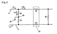
- An end of one of the windings of common mode choke coil 23 is connected to nodal point N2 where impedance element R1 and lead 4 are connected, and the other end is connected to nodal point N4 where impedance element R2 and lead 6 are connected.
- an end of the other winding of common mode choke coil 23 is connected to nodal point N3 where impedance element R1 and lead 5 are connected, and the other end is connected to nodal point N5 where impedance element R2 and lead 7 are connected.
- common mode choke coil 23 is disposed posterior to two impedance elements R1, and impedance element R2 is disposed posterior to common mode choke coil 23.
- Impedance of impedance element R1 connected to lead 4 and that of impedance element R1 connected to lead 5 are set at substantially the same value. Because of such a setting balanced transmission in differential mode can be maintained.
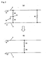
- Fig. 2(a) is a circuit diagram equivalent to balanced transmission termination device 21 of Fig. 1, in differential mode.
- Fig. 2(b) is a circuit diagram equivalent to the circuit of Fig. 2(a).
- balanced transmission termination device 21 becomes equivalent to the circuit shown in Fig. 2(a).
- circuit of Fig. 2(a) is equivalent to that of Fig. 2(b). More specifically, the circuit of Fig. 2(a) is equivalent to that of Fig. 2(b) consisting of two impedance elements R3 connected in series between lead 4 and lead 5.
- R1 impedance of impedance element R1
- R2 impedance of impedance element R2
- R3 resistance of impedance element R3
- R3 is a composite impedance of R1 and R2/2. Therefore, it is preferable to determine values of R1 and R2 in such a manner that R3 becomes substantially the same value as Zo/2 when characteristic impedance of balanced transmission line 3 is denoted as "Zo".
- Fig. 3 is a circuit diagram equivalent to balanced transmission termination device 21 of Fig. 1, in common mode.
- impedance of common mode choke coil 23 becomes greater since magnetic fluxes will participate as in the case of Fig. 5(b).
- balanced transmission termination device 21 becomes equivalent to the circuit of Fig. 3.
- ZC stands for impedance of a winding that constitutes common mode choke coil 23.
- ZC of [Formula 2] is substituted with impedance ZC of common mode choke coil 23 for use.
- An impedance value obtained when a current of a certain frequency is applied to common mode choke coil 23 is adopted as impedance ZC of common mode choke coil 23.
- rated current Ir corresponds to a current level above which a common mode choke coil will be saturated and will no longer be able to effectively perform its function.
- rated current Ir a rated current of a common mode choke coil is specified by the manufacturer of the common mode choke coil.
- rated current Ir herein referred to does not necessarily have to correspond with a rated current specified by the manufacturer.
- impedance of two impedance elements R1 is set at substantially the same value
- impedance of R3 that is a composite impedance of R1 and R2/2 is set at substantially the same value as Zo/2.
- common mode choke coil 23 can effectively perform its function of attenuating common mode noise even when an excessive common mode current is generated in balanced transmission line 3. Also, influence of common mode noise to main body circuit 22 in receiver unit 2 can be minimized.
- each of the impedance elements R1 is a resistance element.
- This prior art is related to a balanced-to-unbalanced transducer comprising a transformer (corresponding to a common mode choke coil).
- common mode noise is sent to a ground through an impedance element disposed between signal lines on the balanced side, for preventing influence of common mode noise.
- the prior art cannot be associated with such an object as preventing saturation of a transformer by restraining the flow of common mode current into the transformer.
- resistance elements are used as impedance elements R1 and R2 in Fig. 1, capacitors or inductors, or a combination thereof can also be employed instead, without limiting resistance elements.
Landscapes
- Engineering & Computer Science (AREA)
- Computer Networks & Wireless Communication (AREA)
- Signal Processing (AREA)
- Dc Digital Transmission (AREA)
- Cable Transmission Systems, Equalization Of Radio And Reduction Of Echo (AREA)
- Input Circuits Of Receivers And Coupling Of Receivers And Audio Equipment (AREA)
- Filters And Equalizers (AREA)
Claims (8)
- Symmetrische-Übertragungs-Endvorrichtung (21), die am Ende einer symmetrischen Übertragungsleitung (3) vorgesehen ist, die aus einem Paar Leitungen (4. 5) besteht, mit:zwei primären Impedanzelementen (R1), die zwischen dem Paar Leitungen (4, 5) in Reihe geschaltet sind, mit einem geerdeten Knotenpunkt (N1) dazwischen, wobei die primären Impedanzelemente (R1) eine Impedanz haben, die die symmetrische Übertragung im Gegentakt aufrechterhalten kann; undeiner Gleichtakt-Drosselspule (23), die in Kaskade nach den primären Impedanzelementen (R1) angeordnet ist, zum Unterdrücken eines in der symmetrischen Übertragungsleitung (3) erzeugten Gleichtaktrauschens,gekennzeichnet durch ein sekundäres Impedanzelement (R2), das in Kaskade nach der Gleichtakt-Drosselspule (23) angeordnet ist, zur Impedanzanpassung an die primären Impedanzelemente (R1), wobei die primären und sekundären Impedanzelemente (R1, R2) eine Impedanz haben, mit der eine Impedanzanpassung an eine charakteristische Impedanz der symmetrischen Übertragungsleitung (3) möglich ist, und die Impedanzen der Gleichtakt-Drosselspule (23), der primären lmpedanzelemente (R1) und des sekundären Impedanzelements (R2) so festgelegt sind, dass ein Gleichtaktstrom, der in die Gleichtakt-Drosselspule (23) fließt, einen vorgegebenen Wert nicht überschreitet.
- Symmetrische-Übertragungs-Endvorrichtung (21) nach Anspruch 1, dadurch gekennzeichnet, dass
die Impedanz der beiden primären Impedanzelemente (R1) auf im Wesentlichen den gleichen Wert eingestellt ist und
die Werte von "R1", "R2" und "ZC" so festgelegt sind, dass sie Folgendes erfüllen:

worin "Zo" für die charakteristische Impedanz der symmetrischen Übertragungsleitung (3) steht, "R1" für die Impedanz des primären Impedanzelements (R1) steht, "R2" für die Impedanz des sekundären Impedanzelements (R2) steht, "ZC" für die Impedanz einer der Wicklungen der Gleichtakt-Drosselspule (23) steht, "Ic" für einen angenommenen Wert des Gleichtaktstroms steht und "Ir" für einen vorgegebenen Wert steht, der einem Nennstromwert der Gleichtakt-Drosselspule (23) entspricht. - Symmetrische-Übertragungs-Endvorrichtung (21) nach Anspruch 1, dadurch gekennzeichnet, dass jedes der primären Impedanzelemente (R1) ein Widerstandselement ist.
- Symmetrische-Übertragungs-Endvorrichtung (21) nach Anspruch 2, dadurch gekennzeichnet, dass jedes der primären Impedanzelemente (R1) ein Widerstandselement ist.
- Empfangseinheit (2) mit der Symmetrische-Übertragungs-Endvorrichtung (21) nach Anspruch 1.
- Empfangseinheit (2) nach Anspruch 5, dadurch gekennzeichnet, dass bei der Symmetrische-Übertragungs-Endvorrichtung (21)
die Impedanz der beiden primären Impedanzelemente (R1) auf im Wesentlichen den gleichen Wert eingestellt ist und
die Werte von "R1", "R2" und "ZC" so festgelegt sind, dass sie Folgendes erfüllen:

worin "Zo" für die charakteristische Impedanz der symmetrischen Übertragungsleitung (3) steht, "R1" für die Impedanz des primären Impedanzelements (R1) steht, "R2" für die Impedanz des sekundären Impedanzelements (R2) steht, "ZC" für die Impedanz einer der Wicklungen der Gleichtakt-Drosselspule (23) steht, "Ic" für einen angenommenen Wert des Gleichtaktstroms steht und "Ir" für einen vorgegebenen Wert steht, der einem Nennstromwert der Gleichtakt-Drosselspule (23) entspricht. - Empfangseinheit (2) nach Anspruch 5, dadurch gekennzeichnet, dass jedes der primären Impedanzelemente (R1), die in der Symmetrische-Übertragungs-Endvorrichtung (21) angeordnet sind, ein Widerstandselement ist.
- Empfangseinheit (2) nach Anspruch 6, dadurch gekennzeichnet, dass jedes der primären Impedanzelemente (R1), die in der Symmetrische-Übertragungs-Endvorrichtung (21) angeordnet sind, ein Widerstandselement ist.
Applications Claiming Priority (2)
| Application Number | Priority Date | Filing Date | Title |
|---|---|---|---|
| JP2001054226 | 2001-02-28 | ||
| JP2001054226A JP4468602B2 (ja) | 2001-02-28 | 2001-02-28 | 平衡伝送終端装置及びそれを用いた受信装置 |
Publications (2)
| Publication Number | Publication Date |
|---|---|
| EP1237295A1 EP1237295A1 (de) | 2002-09-04 |
| EP1237295B1 true EP1237295B1 (de) | 2006-05-03 |
Family
ID=18914590
Family Applications (1)
| Application Number | Title | Priority Date | Filing Date |
|---|---|---|---|
| EP02003231A Expired - Lifetime EP1237295B1 (de) | 2001-02-28 | 2002-02-20 | Abschulussvorrichtung für Ausgewuchtete Übertragung |
Country Status (5)
| Country | Link |
|---|---|
| US (1) | US6677829B2 (de) |
| EP (1) | EP1237295B1 (de) |
| JP (1) | JP4468602B2 (de) |
| KR (1) | KR100821422B1 (de) |
| DE (1) | DE60211052T2 (de) |
Families Citing this family (12)
| Publication number | Priority date | Publication date | Assignee | Title |
|---|---|---|---|---|
| WO2004062220A1 (ja) * | 2002-12-27 | 2004-07-22 | Matsushita Electric Industrial Co., Ltd. | 受信器 |
| US7430291B2 (en) * | 2003-09-03 | 2008-09-30 | Thunder Creative Technologies, Inc. | Common mode transmission line termination |
| JP2005245118A (ja) * | 2004-02-26 | 2005-09-08 | Mitsubishi Electric Corp | インバータ回路を備えた電気装置 |
| US7385466B2 (en) | 2004-03-30 | 2008-06-10 | Matsushita Electric Industrial Co., Ltd. | Differential transmission circuit and common mode choke coil |
| KR100681131B1 (ko) * | 2004-12-02 | 2007-02-08 | 주식회사 로템 | 전동차의 siv 모니터 카드용 노이즈 억제 회로 |
| US7339443B2 (en) * | 2004-12-06 | 2008-03-04 | Matsushita Electric Industrial Co., Ltd. | Common mode radiation inhibit circuit and electronic equipment |
| CN1787504B (zh) * | 2004-12-10 | 2011-05-04 | 松下电器产业株式会社 | 差动传送线路的辐射噪音抑制电路 |
| US7388449B2 (en) * | 2004-12-10 | 2008-06-17 | Matsushita Electric Industrial Co., Ltd. | Radiation noise suppression circuit for differential transmission line |
| JP5386055B2 (ja) * | 2005-08-30 | 2014-01-15 | 株式会社日立製作所 | 特性評価装置および特性評価方法 |
| JP2007274884A (ja) * | 2006-02-02 | 2007-10-18 | Fuji Electric Device Technology Co Ltd | 電力変換装置 |
| US7436203B1 (en) * | 2007-04-18 | 2008-10-14 | National Semiconductor Corporation | On-chip transformer arrangement |
| US20090058559A1 (en) * | 2007-08-31 | 2009-03-05 | Pakkala William F | Microprocessor common-mode emissions reduction circuit |
Family Cites Families (7)
| Publication number | Priority date | Publication date | Assignee | Title |
|---|---|---|---|---|
| US4283604A (en) * | 1979-06-04 | 1981-08-11 | Tellabs, Inc. | Current source circuits with common mode noise rejection |
| DE68927866T2 (de) * | 1988-01-14 | 1997-09-04 | Toshiba Kawasaki Kk | Methode zur Wertbestimmung für Leitungsfilter und zugehörige Komponenten |
| JPH0333424A (ja) | 1989-06-29 | 1991-02-13 | Fuji Heavy Ind Ltd | 筒内直噴式2サイクルエンジン |
| US5179362A (en) * | 1989-12-15 | 1993-01-12 | Kabushiki Kaisha Toshiba | Power line filter |
| JP3033424B2 (ja) | 1994-02-28 | 2000-04-17 | 松下電工株式会社 | 平衡−不平衡変換器 |
| JPH11505677A (ja) * | 1994-08-03 | 1999-05-21 | マッジ・ネットワークス・リミテッド | 電磁妨害アイソレータ |
| US6150896A (en) * | 1994-12-19 | 2000-11-21 | Bh Electronics, Inc. | Coupling device connecting an unbalanced signal line to a balanced signal line |
-
2001
- 2001-02-28 JP JP2001054226A patent/JP4468602B2/ja not_active Expired - Lifetime
-
2002
- 2002-02-20 EP EP02003231A patent/EP1237295B1/de not_active Expired - Lifetime
- 2002-02-20 DE DE60211052T patent/DE60211052T2/de not_active Expired - Lifetime
- 2002-02-27 KR KR1020020010361A patent/KR100821422B1/ko not_active Expired - Lifetime
- 2002-02-27 US US10/086,185 patent/US6677829B2/en not_active Expired - Lifetime
Also Published As
| Publication number | Publication date |
|---|---|
| US20020145485A1 (en) | 2002-10-10 |
| DE60211052T2 (de) | 2006-11-02 |
| EP1237295A1 (de) | 2002-09-04 |
| JP4468602B2 (ja) | 2010-05-26 |
| US6677829B2 (en) | 2004-01-13 |
| DE60211052D1 (de) | 2006-06-08 |
| KR100821422B1 (ko) | 2008-04-10 |
| JP2002261842A (ja) | 2002-09-13 |
| KR20020070134A (ko) | 2002-09-05 |
Similar Documents
| Publication | Publication Date | Title |
|---|---|---|
| EP1237295B1 (de) | Abschulussvorrichtung für Ausgewuchtete Übertragung | |
| US20030095036A1 (en) | Power line communication system and power line branching apparatus | |
| EP0096965B1 (de) | Übertragerunterstützte Leitungsspeiseschaltung aktiver Impedanz | |
| CA1226919A (en) | Receiving circuit for a data transmission system | |
| JPH08115820A (ja) | コモンモードチョークコイル | |
| EP0098066B1 (de) | Datenübertragungssystem | |
| US4951312A (en) | Balanced transmission device | |
| JPH1168497A (ja) | コモンモードフィルタ | |
| EP1465218B1 (de) | Elektrisches gerät mit einem rauschfilter und luftklimatisierer mit solchem gerät | |
| EP0876667B1 (de) | Verfahren zum schutz vor potentialverschiebung der masse und gerät | |
| US4998079A (en) | Bi-directional signal coupler for a balanced data transmission line | |
| US4453131A (en) | Transformer coupled amplifier circuit | |
| US6087822A (en) | Power transformer with internal differential mode distortion cancellation | |
| JP3164567B2 (ja) | ノイズフィルタ | |
| JPH07297035A (ja) | 雑音除去ユニット及びそのユニットを用いた伝送システム | |
| JP3303047B2 (ja) | 妨害波印加装置 | |
| JP2675584B2 (ja) | イミュニティ試験回路 | |
| JP3243674B2 (ja) | Cm型方向性結合器 | |
| JPS6177445A (ja) | 回線結合回路 | |
| JPS5975172A (ja) | ソナ−の送受波器駆動回路 | |
| JPS60250739A (ja) | 遠隔制御用端末器 | |
| JPH07321717A (ja) | 伝送装置 | |
| JPH06163261A (ja) | 集積回路装置 | |
| JPS6224606A (ja) | 分岐トランス | |
| JPH02243040A (ja) | 差動信号伝送路の絶縁方法 |
Legal Events
| Date | Code | Title | Description |
|---|---|---|---|
| PUAI | Public reference made under article 153(3) epc to a published international application that has entered the european phase |
Free format text: ORIGINAL CODE: 0009012 |
|
| AK | Designated contracting states |
Kind code of ref document: A1 Designated state(s): AT BE CH CY DE DK ES FI FR GB GR IE IT LI LU MC NL PT SE TR |
|
| AX | Request for extension of the european patent |
Free format text: AL;LT;LV;MK;RO;SI |
|
| 17P | Request for examination filed |
Effective date: 20020917 |
|
| AKX | Designation fees paid |
Designated state(s): DE FR GB IT SE |
|
| GRAP | Despatch of communication of intention to grant a patent |
Free format text: ORIGINAL CODE: EPIDOSNIGR1 |
|
| GRAS | Grant fee paid |
Free format text: ORIGINAL CODE: EPIDOSNIGR3 |
|
| GRAA | (expected) grant |
Free format text: ORIGINAL CODE: 0009210 |
|
| AK | Designated contracting states |
Kind code of ref document: B1 Designated state(s): DE FR GB IT SE |
|
| PG25 | Lapsed in a contracting state [announced via postgrant information from national office to epo] |
Ref country code: IT Free format text: LAPSE BECAUSE OF FAILURE TO SUBMIT A TRANSLATION OF THE DESCRIPTION OR TO PAY THE FEE WITHIN THE PRESCRIBED TIME-LIMIT;WARNING: LAPSES OF ITALIAN PATENTS WITH EFFECTIVE DATE BEFORE 2007 MAY HAVE OCCURRED AT ANY TIME BEFORE 2007. THE CORRECT EFFECTIVE DATE MAY BE DIFFERENT FROM THE ONE RECORDED. Effective date: 20060503 |
|
| REG | Reference to a national code |
Ref country code: GB Ref legal event code: FG4D |
|
| REF | Corresponds to: |
Ref document number: 60211052 Country of ref document: DE Date of ref document: 20060608 Kind code of ref document: P |
|
| REG | Reference to a national code |
Ref country code: SE Ref legal event code: TRGR |
|
| ET | Fr: translation filed | ||
| PLBE | No opposition filed within time limit |
Free format text: ORIGINAL CODE: 0009261 |
|
| STAA | Information on the status of an ep patent application or granted ep patent |
Free format text: STATUS: NO OPPOSITION FILED WITHIN TIME LIMIT |
|
| 26N | No opposition filed |
Effective date: 20070206 |
|
| REG | Reference to a national code |
Ref country code: FR Ref legal event code: PLFP Year of fee payment: 15 |
|
| REG | Reference to a national code |
Ref country code: FR Ref legal event code: PLFP Year of fee payment: 16 |
|
| REG | Reference to a national code |
Ref country code: FR Ref legal event code: PLFP Year of fee payment: 17 |
|
| PGFP | Annual fee paid to national office [announced via postgrant information from national office to epo] |
Ref country code: FR Payment date: 20210112 Year of fee payment: 20 |
|
| PGFP | Annual fee paid to national office [announced via postgrant information from national office to epo] |
Ref country code: SE Payment date: 20210210 Year of fee payment: 20 Ref country code: DE Payment date: 20210209 Year of fee payment: 20 Ref country code: GB Payment date: 20210210 Year of fee payment: 20 |
|
| PGFP | Annual fee paid to national office [announced via postgrant information from national office to epo] |
Ref country code: IT Payment date: 20210112 Year of fee payment: 20 |
|
| REG | Reference to a national code |
Ref country code: DE Ref legal event code: R071 Ref document number: 60211052 Country of ref document: DE |
|
| REG | Reference to a national code |
Ref country code: GB Ref legal event code: PE20 Expiry date: 20220219 |
|
| REG | Reference to a national code |
Ref country code: SE Ref legal event code: EUG |
|
| PG25 | Lapsed in a contracting state [announced via postgrant information from national office to epo] |
Ref country code: GB Free format text: LAPSE BECAUSE OF EXPIRATION OF PROTECTION Effective date: 20220219 |