EP1237197A2 - Matrix von Phototransistoren aus amorphem Halbleitermaterial mit offener Basis - Google Patents
Matrix von Phototransistoren aus amorphem Halbleitermaterial mit offener Basis Download PDFInfo
- Publication number
- EP1237197A2 EP1237197A2 EP01127030A EP01127030A EP1237197A2 EP 1237197 A2 EP1237197 A2 EP 1237197A2 EP 01127030 A EP01127030 A EP 01127030A EP 01127030 A EP01127030 A EP 01127030A EP 1237197 A2 EP1237197 A2 EP 1237197A2
- Authority
- EP
- European Patent Office
- Prior art keywords
- layer
- phototransistor
- bipolar
- amorphous semiconductor
- phototransistors
- Prior art date
- Legal status (The legal status is an assumption and is not a legal conclusion. Google has not performed a legal analysis and makes no representation as to the accuracy of the status listed.)
- Withdrawn
Links
Images


Classifications
-
- H—ELECTRICITY
- H10—SEMICONDUCTOR DEVICES; ELECTRIC SOLID-STATE DEVICES NOT OTHERWISE PROVIDED FOR
- H10F—INORGANIC SEMICONDUCTOR DEVICES SENSITIVE TO INFRARED RADIATION, LIGHT, ELECTROMAGNETIC RADIATION OF SHORTER WAVELENGTH OR CORPUSCULAR RADIATION
- H10F77/00—Constructional details of devices covered by this subclass
- H10F77/10—Semiconductor bodies
- H10F77/16—Material structures, e.g. crystalline structures, film structures or crystal plane orientations
- H10F77/162—Non-monocrystalline materials, e.g. semiconductor particles embedded in insulating materials
- H10F77/166—Amorphous semiconductors
-
- H—ELECTRICITY
- H10—SEMICONDUCTOR DEVICES; ELECTRIC SOLID-STATE DEVICES NOT OTHERWISE PROVIDED FOR
- H10F—INORGANIC SEMICONDUCTOR DEVICES SENSITIVE TO INFRARED RADIATION, LIGHT, ELECTROMAGNETIC RADIATION OF SHORTER WAVELENGTH OR CORPUSCULAR RADIATION
- H10F39/00—Integrated devices, or assemblies of multiple devices, comprising at least one element covered by group H10F30/00, e.g. radiation detectors comprising photodiode arrays
- H10F39/10—Integrated devices
- H10F39/12—Image sensors
- H10F39/197—Bipolar transistor image sensors
-
- Y—GENERAL TAGGING OF NEW TECHNOLOGICAL DEVELOPMENTS; GENERAL TAGGING OF CROSS-SECTIONAL TECHNOLOGIES SPANNING OVER SEVERAL SECTIONS OF THE IPC; TECHNICAL SUBJECTS COVERED BY FORMER USPC CROSS-REFERENCE ART COLLECTIONS [XRACs] AND DIGESTS
- Y02—TECHNOLOGIES OR APPLICATIONS FOR MITIGATION OR ADAPTATION AGAINST CLIMATE CHANGE
- Y02E—REDUCTION OF GREENHOUSE GAS [GHG] EMISSIONS, RELATED TO ENERGY GENERATION, TRANSMISSION OR DISTRIBUTION
- Y02E10/00—Energy generation through renewable energy sources
- Y02E10/50—Photovoltaic [PV] energy
Definitions
- the invention relates generally to imaging arrays and more particularly to enhancing the sensitivity of photosensors to incoming light.
- a one-dimensional array or a two-dimensional array of imaging sensors may be connected to processing circuitry in order to generate image information relating to an area at which the array is directed.
- Each sensor generates a signal that is responsive to the light received at the sensor.
- the signal may represent intensities of colors of light received by the sensor.
- Charged coupled devices are used in many imaging applications.
- An element of a CCD array integrates a charge that is generated by incoming light, with the charge being accumulated in a potential well along the surface of a semiconductor chip on which the CCD array is fabricated.
- the accumulated charges of the array are sequentially shifted to on-chip circuitry that transfers the signals to other circuitry that is not integrated onto the chip.
- the "gain” that is experienced at each element is less than one.
- the gain may be measured at the current level (output current/photon current) or at the electron level (output electrons/input photons). With a gain at the electron level that has a maximum of unity, the signal-to-noise ratio at the output of a particular element is limited.
- a pixel interconnect structure is formed on the top surface of a substrate, such as a silicon substrate.
- the pixel interconnect structure is a dielectric layer, such as silicon oxide or silicon nitride, having conductive vias extending from selected locations on the surface of the substrate to bottom electrodes of an array of photosensors.
- the bottom electrodes are formed of amorphous silicon having an n-type dopant.
- a continuous intrinsic layer is formed over the bottom electrodes.
- a continuous layer of p-doped amorphous silicon covers the intrinsic layer, while a transparent conductor covers the p-doped layer.
- a PIN diode is formed for each one of the bottom electrodes.
- the PIN diodes are "elevated" sensors, since they are positioned above the surface of the substrate.
- the pixel interconnect structure allows the elevated PIN diodes to be electrically linked to processing circuitry that is fabricated at the substrate level.
- Bipolar phototransistors are fabricated by introducing dopants into a silicon substrate. Conventional dopant implantation steps are utilized. When an array of the bipolar phototransistors is formed, the bases of the phototransistors in a particular row are capacitively coupled to a common row-select line. The emitters of all the phototransistors in a particular column are connected to a common column-select line. Thus, each phototransistor can be individually selected. The array of phototransistors provides greater gain than is available using CCD technology.
- An object of the invention is to provide an imaging arrangement in which individual photosensors in an array of photosensors achieve a relatively high level of gain, so that a desired signal-to-noise ratio can be obtained.
- bipolar phototransistors Light sensitivity for imaging applications is enhanced by utilizing bipolar phototransistors that are formed of multiple amorphous semiconductor layers.
- the bipolar phototransistors are open base devices in which holes that are generated by incoming photons provide base-hole current injection, so as to achieve bipolar gain for the photocurrent.
- each phototransistor is formed of amorphous silicon emitter, base and collector layers, but other amorphous semiconductive materials (such as the semiconducting polymer of fluorene-bithiophene copolymer) may be substituted.
- the base and emitter layers are doped to form either an NPN bipolar transistor or a PNP bipolar transistor, while the collector layer is either undoped or is very lightly doped, i.e., the collector layer is an intrinsic layer.
- the emitter layer may be a first-deposited layer of amorphous silicon with a heavy concentration of an n-type dopant.
- the base layer is deposited over the emitter layer as an amorphous silicon having a p-type dopant.
- the collector layer may be a continuous amorphous silicon layer or may be a layer in which a dielectric separates each pixel from adjacent pixels.
- a thin layer of n-doped amorphous silicon is formed atop the intrinsic collector layer.
- a transparent top electrode is deposited. While the emitter layer may function as the bottom electrode, preferably a separate electrode layer is formed prior to depositing the layers that define the bipolar transistors. In the PNP application, the conductivity types of the base and emitter layers are reversed, as well as the conductivity type of the thin layer above the intrinsic collector layer.
- Each phototransistor may be operated in an integrating mode in which the total bipolar current is integrated for periodic reading.
- each phototransistor may be operated in a static mode in which a signal is sensed by monitoring the voltage at a particular node.
- the phototransistor is an open base device.
- the base layer is free from external control.
- holes and electrons are generated within the layer.
- the holes that are generated by the photons are conducted to the base layer to serve as base-hole current injection.
- bipolar gain is achieved.
- the array of phototransistors is preferably formed on the same substrate as processing circuitry for sensing and/or amplifying output signals for transfer to off-substrate circuitry.
- An advantage of the invention is that the current gain achieved at the phototransistor level enhances the sensitivity of the arrangement. Output fluctuations as a result of changes in light intensity are more easily distinguished from "noise.”
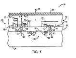
- a pair of NPN phototransistors 10 and 12 of an array 14 of phototransistors is formed of a number of different amorphous semiconductor layers.
- the amorphous semiconductor layers will be described as being formed of amorphous silicon. However, other materials are suitable, such as the organic semiconductor fluorene-bithiophene copolymer.
- an emitter 16 is an n ++ layer
- a base 18 is a p + layer
- a collector 20 is an intrinsic layer.
- a fourth amorphous silicon layer 22 is formed atop the intrinsic collector layer. This fourth layer has an n + conductivity type.
- the amorphous layers that form the emitter 16, the base 18 and the collector 20 are deposited over a substrate 24, such as a silicon substrate, in which processing circuitry is formed.
- the processing circuitry is represented by a single transistor 26 having source/drain regions 28 and 30 and having a gate 32.
- the source/drain regions are formed by ion implantation, while the gate 32 is fabricated by depositing a polysilicon layer atop an oxide layer.
- the transistor is formed between two field oxide regions (FOX) 34 and 36.
- a pixel interconnect structure 38 Connectivity between the phototransistors 10 and 12 and the processing circuitry that is embedded within the substrate 24 is provided by a pixel interconnect structure 38, such as the type described above with reference to U.S. Pat. No. 6,018,187 to Theil et al. Electrodes 40 and 42 atop the pixel interconnect structure 38 are aligned with conductive vias 44 and 46 through the interconnect structure. The vias electrically connect the electrodes to conductive paths 48 and 50 on the surface of the substrate 24. As will be described more fully below, the conductive paths are connected to underlying circuitry of the substrate 24 or to external circuitry. The circuit connections are represented as nodes 52 and 54, which may be floating nodes.
- the nodes 52 and 54 may be selectively reset at a level lower than electrical "high" when the phototransistors are operated in an integrating mode for monitoring the voltage change across the two nodes 52 and 54.
- a top electrode layer 56 is connected to V DD or another high voltage constant by connection to node 58.
- the process circuitry formed at the level of the substrate 24 may be provided using known techniques.
- the circuitry may be CMOS (Complementary Metal Oxide Silicon), BiCMOS or Bipolar.
- the pixel interconnect structure 38 may be a layer of silicon oxide or silicon nitride, with the vias 44 and 46 being formed of tungsten. Tungsten vias enable narrow and relatively long interconnections to be made.
- the tungsten vias may be formed using a chemical vapor deposition (CVD) process. However, other materials and other processes may be substituted.
- CVD chemical vapor deposition
- the electrodes 40 and 42 are formed of more than one layer.
- a lower metal layer of titanium or tungsten having a thickness of approximately 500 Angstroms may be used to enhance current collection from a doped semiconductor upper layer of the electrodes.
- the doped semiconductor can be amorphous silicon having n-type conductivity. If a doped semiconductor material is used, the layer must have a sufficient thickness and dopant concentration to prevent the material from being fully depleted when biased during operation.
- electrodes 40 and 42 are not necessary in all applications, since the emitter 16 may be formed to contact the vias 44 and 46 or to contact the thin metal layer that is in direct contact with the vias.
- the layers that form the emitter 16, base 18 and collector 20, as well as the thin layer 22, are preferably amorphous silicon.
- a silicon-containing gas may be used to deposit the layers using plasma enhanced chemical vapor deposition (PECVD).
- PECVD plasma enhanced chemical vapor deposition
- the gas includes hydrogen, so that each of the four layers is amorphous-Si:H.
- an appropriate dopant is included.
- the phosphorous gas PH 3 may be used in forming the base, while the boron gas B 2 H 6 may be used in forming the emitter 16 and the top thin layer 22.
- a number of symbols are included in order to explain the operation of the phototransistor 10.
- Incoming photons are represented by hv.
- the incoming photons will generate electron-hole pairs.
- the flow of the electrons is shown by the arrow associated with the symbol e - ph
- the flow of the holes is represented by the symbol h + ph .
- the flow of electrons and holes as a result of biasing the phototransistor is represented by the systems e - bipolar and h + bipolar , respectively.
- the current gain ( ⁇ ) of the phototransistor 10 may be considered to be I bipolar /I photon , if the recombination of electrons and holes is disregarded.
- the holes h + ph flow to the base 18. These holes serve as base-hole current injection.
- the base is left in an electrically open condition, so that bipolar gain for photocurrent is achieved.
- Figs. 2 and 3 compare the current flow through a conventional photodiode 60 to the current flow through the open base phototransistor 10 of Fig. 1.
- the photodiode 60 generates a current I photon that is directly responsive to the intensity of light received by the photodiode.
- a comparable current is generated from the collector region 20 to the base region 18.
- a current gain is achieved by the flow of current from the V DD node 58 to the electrical ground node 52. While not critical to the invention, the current gain can be set at between 5 and 100, depending upon the application.
- the phototransistor 10 of Figs. 1 and 3 provides a significant improvement over the use of the photodiode 60 of Fig. 2.
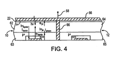
- a continuous base layer and a continuous intrinsic layer that forms the collector regions may be patterned to provide segmented transistors.
- a dielectric 66 isolates the collector 62 and the base 63 of the first phototransistor 10 from the collector 64 and the base 65 of the second phototransistor 12.
- the material selected to form the dielectric is not critical.
- the bases 63 and 65 and the collectors 62 and 64 may be separated by air.
- the n + layer 22 is shown as being divided by the dielectric 66.
- the thin layer 22 may be continuous, since this will not affect operation of the two phototransistors 10 and 12.
- the thin layer 22 and the top electrode layer 56 may both be segmented by the dielectric 66.
- the requirement of separate connections might be undesirable.
- first and second phototransistors 68 and 70 are PNP devices.
- the two phototransistors are shown as having electrodes 72 and 74, but the electrodes may be omitted by utilizing a p ++ emitter 76 as the contact for interconnection with a substrate which is not shown in Fig. 5.
- the emitter is an amorphous silicon layer that is deposited using known techniques, such as PECVD.
- the amorphous silicon layer may be deposited directly on a substrate or may be deposited on a pixel interconnect structure, such as the type described with reference to Fig. 1.
- a second amorphous silicon layer is deposited to function as the open base 78 for each of the two phototransistors 68 and 70.
- Each base includes a dopant having an n + conductivity.
- An intrinsic amorphous silicon layer forms the collector 80 for each of the phototransistors.
- the intrinsic layer includes no intentionally introduced dopant or includes a very low level of dopant.
- a top electrode 84 is formed of a conductive material.
- the operation of the PNP phototransistors 68 and 70 will be readily understood by persons skilled in the art.
- the electrical connections are the reverse of those described with reference to Fig. 1. That is, the top electrode 84 is connected to electrical ground or a constant low level voltage.
- the bottom electrodes 72 and 74 are connected to the floating node of underlying substrate circuitry or external circuitry. Electrons and holes that are generated as a result of incoming photons will propagate in opposite directions, with the propagation to an open base 78 providing current injection that enables the bipolar gain to be responsive to photocurrent.
- the open base phototransistors described with reference to Figs. 1-5 may be operated in an integrating mode in which signals are sensed by integrating the total bipolar current or may be operated in a static mode in which signals are sensed by monitoring the voltage increase at a particular node.
- the integrating mode will be described with reference to Figs. 6 and 7, while the static mode will be described with reference to Figs. 8 and 9.
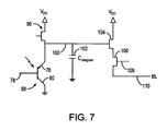
- the NPN phototransistor 10 of Fig. 1 has its emitter 16 connected to a floating node 52 that is linked to electrical ground by an integration capacitor 86 and by a transistor 88.
- the integration capacitor will charge to a potential that is dependent upon the photocurrent through the phototransistor 10.
- the integration capacitor may be an intentionally added circuit element or it may be the parasitic capacitance between the base and the collector of the phototransistor in addition to the other parasitic capacitances connected to the floating node.
- Transistor 88 is used to "reset" the floating node to a potential lower than the high voltage at the beginning of the integration time. The reset is accomplished by turning transistor 88 to the "on” state for a short period and then to the "off” state to begin the integration period.
- the integrated charge may be read via a bit line 90 by operation of a source follower.
- Transistors 92 and 94 transfer the voltage on the integration capacitor to the bit line when a write access line 96 receives a signal that turns the transistor 94 to an "on" state.
- an array of photosensors can be serially scanned by selectively activating row-select lines and column-select lines.
- the integration capacitor 86 is charged. It is this charge that is periodically read.
- the integration period is the time between the reset of the floating node and the reception of the appropriate signal at the write access line 96.
- the emitter 16, base 18 and collector 20 are formed by the amorphous silicon layers.
- the transistors 88, 92 and 94 are formed within the silicon substrate 24.
- the transistor 92 in Fig. 6 may be the transistor 26 in Fig. 1, if the conductive path 48 along the surface of the substrate is connected to the gate 32 of the transistor 26.
- the PNP phototransistor 68 of Fig. 5 is shown as having its collector 80 connected to electrical ground and having its emitter 76 connected to a source/drain region of a transistor 98.
- the other source/drain region of the transistor 98 is connected to V DD .
- Transistor 98 is used to reset the floating node 100 to a potential above the electrical ground at the beginning of the integration time.
- the collector 80 of the phototransistor 68 is connected to an integration capacitor 102, which, as before, may be a separate circuit element or the parasitic base-collector capacitance of the phototransistor and the other parasitic capacitances connected to the floating node. The voltage across the integration capacitor depends on the total current through the phototransistor during the integration time.
- This voltage is transferred to a bit line 110 by transistors 104 and 106 when the write line 108 turns the transistor 106 to the "on" state.
- the signal that is transferred to a bit line 110 will be dependent upon the intensity of light received by the phototransistor 68 during an integration time.
- a two-dimensional array of phototransistors may be serially accessed by selectively activating transistors.
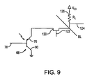
- the open base phototransistor 10 of Fig. 1 is operated in the static mode.
- the circuit monitors the voltage increase at the node 52 connected to the emitter 16 of the phototransistor.
- a signal along a write access line 112 selectively turns a transistor 114 to an "on" state.
- a load resistor 116 is connected between ground and an output line 118.
- V out ( ⁇ + 1) I photon * R L
- the PNP transistor 68 is being used in a static mode operation.
- the voltage along an output line 124 may be read as the output of the phototransistor 68, since the voltage drop across a load resistor 126 will depend upon the current flow through the phototransistor.
- circuits shown in Figs. 6-9 are examples of possible applications for the amorphous silicon open base phototransistors. However, other applications may be utilized without diverging from the invention. Moreover, other amorphous semiconductors may be substituted for the amorphous silicon.
Landscapes
- Light Receiving Elements (AREA)
- Solid State Image Pick-Up Elements (AREA)
- Transforming Light Signals Into Electric Signals (AREA)
Applications Claiming Priority (2)
| Application Number | Priority Date | Filing Date | Title |
|---|---|---|---|
| US795608 | 2001-02-28 | ||
| US09/795,608 US7038242B2 (en) | 2001-02-28 | 2001-02-28 | Amorphous semiconductor open base phototransistor array |
Publications (2)
| Publication Number | Publication Date |
|---|---|
| EP1237197A2 true EP1237197A2 (de) | 2002-09-04 |
| EP1237197A3 EP1237197A3 (de) | 2005-06-22 |
Family
ID=25165988
Family Applications (1)
| Application Number | Title | Priority Date | Filing Date |
|---|---|---|---|
| EP01127030A Withdrawn EP1237197A3 (de) | 2001-02-28 | 2001-11-14 | Matrix von Phototransistoren aus amorphem Halbleitermaterial mit offener Basis |
Country Status (3)
| Country | Link |
|---|---|
| US (1) | US7038242B2 (de) |
| EP (1) | EP1237197A3 (de) |
| JP (2) | JP2002289825A (de) |
Cited By (3)
| Publication number | Priority date | Publication date | Assignee | Title |
|---|---|---|---|---|
| WO2004038809A2 (en) | 2002-10-23 | 2004-05-06 | Goldpower Limited | Formation of contacts on semiconductor substrates |
| EP1677354A1 (de) * | 2004-12-30 | 2006-07-05 | DongbuAnam Semiconductor Inc. | CMOS Bildsensor und dessen Herstellungsmethode |
| DE102014115464A1 (de) | 2014-10-23 | 2016-04-28 | Infineon Technologies Austria Ag | Leistungs-halbleitervorrichtung mit temperaturschutz |
Families Citing this family (22)
| Publication number | Priority date | Publication date | Assignee | Title |
|---|---|---|---|---|
| TW538504B (en) * | 2002-06-20 | 2003-06-21 | Twinhan Technology Co Ltd | Current amplification of logarithmic mode CMOS image sensor |
| US7768500B2 (en) * | 2003-06-16 | 2010-08-03 | Humanscale Corporation | Ergonomic pointing device |
| US7557799B2 (en) | 2004-06-17 | 2009-07-07 | Avago Technologies Ecbu Ip (Singapore) Pte. Ltd. | System for determining pointer position, movement, and angle |
| WO2008106764A1 (en) * | 2007-03-05 | 2008-09-12 | Arokia Nathan | Sensor pixels, arrays and array systems and methods therefor |
| US8587081B2 (en) * | 2010-04-28 | 2013-11-19 | Calvin Yi-Ping Chao | Back side illuminated image sensor with back side pixel substrate bias |
| GB2481227A (en) * | 2010-06-16 | 2011-12-21 | Cambridge Display Tech Ltd | An organic electroluminescent device comprising a plasticiser |
| US8753917B2 (en) * | 2010-12-14 | 2014-06-17 | International Business Machines Corporation | Method of fabricating photoconductor-on-active pixel device |
| US8809897B2 (en) | 2011-08-31 | 2014-08-19 | Micron Technology, Inc. | Solid state transducer devices, including devices having integrated electrostatic discharge protection, and associated systems and methods |
| US9490239B2 (en) * | 2011-08-31 | 2016-11-08 | Micron Technology, Inc. | Solid state transducers with state detection, and associated systems and methods |
| FR2983296B1 (fr) * | 2011-11-29 | 2013-12-27 | Soc Fr Detecteurs Infrarouges Sofradir | Dispositif de detection de rayonnement a etendue d'illumination amelioree |
| JP2015159133A (ja) * | 2012-06-14 | 2015-09-03 | シャープ株式会社 | 受光装置 |
| US10094988B2 (en) * | 2012-08-31 | 2018-10-09 | Micron Technology, Inc. | Method of forming photonics structures |
| JP6354221B2 (ja) * | 2014-03-12 | 2018-07-11 | 株式会社リコー | 撮像装置及び電子機器 |
| WO2016010292A1 (en) * | 2014-07-15 | 2016-01-21 | Vieworks Co., Ltd. | Radiation detector |
| KR102282493B1 (ko) * | 2014-08-12 | 2021-07-26 | 삼성전자주식회사 | 이미지 센서 및 이를 포함하는 전자 장치 |
| US10192892B2 (en) | 2015-05-29 | 2019-01-29 | Palo Alto Research Center Incorporated | Active matrix backplane formed using thin film optocouplers |
| US9946135B2 (en) | 2015-05-29 | 2018-04-17 | Palo Alto Research Center Incorporated | High voltage thin film optical switch |
| US10397529B2 (en) | 2017-04-28 | 2019-08-27 | Palo Alto Research Center Incorporated | Transparent optical coupler active matrix array |
| US10388647B1 (en) * | 2018-08-20 | 2019-08-20 | Amazing Microelectronic Corp. | Transient voltage suppression device |
| TW202018971A (zh) * | 2018-11-02 | 2020-05-16 | 美祿科技股份有限公司 | 光電晶體及光電晶體陣列 |
| US11791334B2 (en) | 2020-10-20 | 2023-10-17 | Globalfoundries U.S. Inc. | Heterojunction bipolar transistor with buried trap rich isolation region |
| US12237407B2 (en) | 2022-11-01 | 2025-02-25 | Globalfoundries U.S. Inc. | Heterojunction bipolar transistor with amorphous semiconductor regions |
Family Cites Families (26)
| Publication number | Priority date | Publication date | Assignee | Title |
|---|---|---|---|---|
| JPS55140266A (en) * | 1979-04-20 | 1980-11-01 | Hitachi Ltd | Semiconductor device |
| US4341954A (en) * | 1980-02-06 | 1982-07-27 | Nippon Telegraph & Telephone Public Corp. | Photo-electric converting apparatus |
| JPS5814569A (ja) * | 1981-07-17 | 1983-01-27 | Olympus Optical Co Ltd | カラ−撮像装置 |
| JPS6161457A (ja) | 1984-09-01 | 1986-03-29 | Canon Inc | 光センサおよびその製造方法 |
| US5268309A (en) | 1984-09-01 | 1993-12-07 | Canon Kabushiki Kaisha | Method for manufacturing a photosensor |
| FR2623038B1 (fr) * | 1987-11-10 | 1994-05-20 | Thomson Csf | Matrice d'elements photosensibles associant un phototransistor et une capacite de stockage |
| US5311047A (en) * | 1988-11-16 | 1994-05-10 | National Science Council | Amorphous SI/SIC heterojunction color-sensitive phototransistor |
| JPH02210877A (ja) * | 1989-02-10 | 1990-08-22 | Seiko Epson Corp | 固体撮像装置 |
| US4996573A (en) | 1989-10-27 | 1991-02-26 | Xerox Corporation | Vertical thin film transistor and optical sensor having leakage current suppression elements |
| US5324958A (en) | 1991-02-19 | 1994-06-28 | Synaptics, Incorporated | Integrating imaging systgem having wide dynamic range with sample/hold circuits |
| JPH04275467A (ja) * | 1991-03-04 | 1992-10-01 | Sanyo Electric Co Ltd | フォトトランジスタ |
| JPH05130510A (ja) * | 1991-11-05 | 1993-05-25 | Nippon Sheet Glass Co Ltd | イメージセンサ |
| JPH0643482A (ja) * | 1992-07-24 | 1994-02-18 | Matsushita Electric Ind Co Ltd | 空間光変調素子およびその製造方法 |
| US5321294A (en) * | 1992-08-31 | 1994-06-14 | Matsushita Electric Industrial Co., Ltd. | Shift register having optically bistable elements coupled by an optical waveguide layer |
| JP2985731B2 (ja) * | 1995-05-31 | 1999-12-06 | 松下電器産業株式会社 | X線撮像装置 |
| US6058223A (en) * | 1996-06-27 | 2000-05-02 | The Johns Hopkins University | Video-centroid integrated circuit |
| JP3577368B2 (ja) * | 1995-08-25 | 2004-10-13 | 株式会社東芝 | ハイブリッド型赤外線検出器 |
| AU6388796A (en) * | 1995-09-11 | 1997-04-01 | Analog Devices, Inc. | Electrostatic discharge protection network and method |
| IL125291A (en) * | 1996-01-11 | 2003-01-12 | Univ Princeton | Organic luminescent coating for light detectors |
| DE19613820A1 (de) | 1996-04-09 | 1997-10-23 | Forschungszentrum Juelich Gmbh | Struktur mit einer pin- oder nip-Schichtenfolge |
| US5734191A (en) * | 1996-08-13 | 1998-03-31 | National Semiconductor Corporation | Contactless capacitor-coupled bipolar active pixel sensor with integrated electronic shutter |
| US5885498A (en) * | 1996-12-11 | 1999-03-23 | Matsushita Electric Industrial Co., Ltd. | Organic light emitting device and method for producing the same |
| JP3649907B2 (ja) * | 1998-01-20 | 2005-05-18 | シャープ株式会社 | 二次元画像検出器およびその製造方法 |
| US6018187A (en) | 1998-10-19 | 2000-01-25 | Hewlett-Packard Cmpany | Elevated pin diode active pixel sensor including a unique interconnection structure |
| JP2001036059A (ja) * | 1999-07-22 | 2001-02-09 | Minolta Co Ltd | 固体撮像装置 |
| US6455836B1 (en) * | 2000-04-25 | 2002-09-24 | Agilent Technologies, Inc. | Metallic optical barrier for photo-detector array is also interconnecting electrode |
-
2001
- 2001-02-28 US US09/795,608 patent/US7038242B2/en not_active Expired - Lifetime
- 2001-11-14 EP EP01127030A patent/EP1237197A3/de not_active Withdrawn
-
2002
- 2002-02-18 JP JP2002039731A patent/JP2002289825A/ja active Pending
-
2007
- 2007-11-28 JP JP2007307361A patent/JP2008141198A/ja active Pending
Non-Patent Citations (1)
| Title |
|---|
| NAKAMURA YOSHIO ET AL: "DESIGN OF BIPOLAR IMAGING DEVICE (BASIS)", IEEE TRANSACTIONS ON ELECTRON DEVICES, IEEE SERVICE CENTER, PISACATAWAY, NJ, US, vol. 38, no. 5, 1 May 1991 (1991-05-01), pages 1028 - 1036, XP000200657, ISSN: 0018-9383 * |
Cited By (9)
| Publication number | Priority date | Publication date | Assignee | Title |
|---|---|---|---|---|
| WO2004038809A2 (en) | 2002-10-23 | 2004-05-06 | Goldpower Limited | Formation of contacts on semiconductor substrates |
| USRE43948E1 (en) | 2002-10-23 | 2013-01-29 | Siemens Aktiengesellschaft | Formation of contacts on semiconductor substrates |
| EP1554759B1 (de) * | 2002-10-23 | 2015-10-07 | Siemens Aktiengesellschaft | Herstellung von kontakten auf halbleitersubstraten |
| EP1677354A1 (de) * | 2004-12-30 | 2006-07-05 | DongbuAnam Semiconductor Inc. | CMOS Bildsensor und dessen Herstellungsmethode |
| US7442572B2 (en) | 2004-12-30 | 2008-10-28 | Dongbu Electronic Co., Ltd. | CMOS image sensor and method for manufacturing the same |
| US7745862B2 (en) | 2004-12-30 | 2010-06-29 | Dongbu Electronics Co., Ltd. | CMOS image sensor and method for manufacturing the same |
| DE102014115464A1 (de) | 2014-10-23 | 2016-04-28 | Infineon Technologies Austria Ag | Leistungs-halbleitervorrichtung mit temperaturschutz |
| DE102014115464B4 (de) | 2014-10-23 | 2019-10-24 | Infineon Technologies Austria Ag | Leistungs-halbleitervorrichtung mit temperaturschutz |
| US11276680B2 (en) | 2014-10-23 | 2022-03-15 | Infineon Technologies Austria Ag | Power semiconductor device with integrated temperature protection |
Also Published As
| Publication number | Publication date |
|---|---|
| US20020117682A1 (en) | 2002-08-29 |
| US7038242B2 (en) | 2006-05-02 |
| JP2008141198A (ja) | 2008-06-19 |
| EP1237197A3 (de) | 2005-06-22 |
| JP2002289825A (ja) | 2002-10-04 |
Similar Documents
| Publication | Publication Date | Title |
|---|---|---|
| US7038242B2 (en) | Amorphous semiconductor open base phototransistor array | |
| US5260592A (en) | Integrating photosensor and imaging system having wide dynamic range with varactors | |
| US7541627B2 (en) | Method and apparatus for improving sensitivity in vertical color CMOS image sensors | |
| US5324958A (en) | Integrating imaging systgem having wide dynamic range with sample/hold circuits | |
| US5097305A (en) | Integrating photosensor and imaging system having wide dynamic range | |
| US6927089B2 (en) | CMOS imager and method of formation | |
| EP0978878B1 (de) | Festkörper-Bildaufnahmevorrichtung und Verfahren zum Erfassen eines optischen Signals mit Hilfe einer solchen Vorrichtung | |
| US6040592A (en) | Well to substrate photodiode for use in a CMOS sensor on a salicide process | |
| US5276407A (en) | Sense amplifier | |
| US7772627B2 (en) | Image sensor with floating diffusion gate capacitor | |
| US5705846A (en) | CMOS-compatible active pixel image array using vertical pnp cell | |
| US20090039397A1 (en) | Image sensor structure | |
| US6150704A (en) | Photoelectric conversion apparatus and image sensor | |
| US20040099892A1 (en) | CMOS imager with improved color response | |
| US6396118B1 (en) | Conductive mesh bias connection for an array of elevated active pixel sensors | |
| KR960002100B1 (ko) | 전하결합소자형 이미지센서 | |
| TWI470777B (zh) | 包含具磊晶層之像素單元的影像感測器、具有該影像感測器的系統以及像素單元的形成方法 | |
| US6852566B2 (en) | Self-aligned rear electrode for diode array element | |
| EP0118568B1 (de) | Halbleiter-bildaufzeichnungsvorrichtung | |
| KR100766497B1 (ko) | 이미지 센서 | |
| US20260101626A1 (en) | Device for Light Detection, an Image Sensor, and a Method for Light Detection | |
| KR100321769B1 (ko) | 음의기판전압을갖는씨모스이미지센서의단위화소 |
Legal Events
| Date | Code | Title | Description |
|---|---|---|---|
| PUAI | Public reference made under article 153(3) epc to a published international application that has entered the european phase |
Free format text: ORIGINAL CODE: 0009012 |
|
| AK | Designated contracting states |
Kind code of ref document: A2 Designated state(s): AT BE CH CY DE DK ES FI FR GB GR IE IT LI LU MC NL PT SE TR |
|
| AX | Request for extension of the european patent |
Free format text: AL;LT;LV;MK;RO;SI |
|
| PUAL | Search report despatched |
Free format text: ORIGINAL CODE: 0009013 |
|
| AK | Designated contracting states |
Kind code of ref document: A3 Designated state(s): AT BE CH CY DE DK ES FI FR GB GR IE IT LI LU MC NL PT SE TR |
|
| AX | Request for extension of the european patent |
Extension state: AL LT LV MK RO SI |
|
| RIC1 | Information provided on ipc code assigned before grant |
Ipc: 7H 01L 31/11 B Ipc: 7H 01L 51/20 B Ipc: 7H 01L 31/0376 B Ipc: 7H 01L 27/146 A |
|
| 17P | Request for examination filed |
Effective date: 20051209 |
|
| AKX | Designation fees paid |
Designated state(s): DE FR GB |
|
| RAP1 | Party data changed (applicant data changed or rights of an application transferred) |
Owner name: AVAGO TECHNOLOGIES GENERAL IP (SINGAPORE) PTE. LTD |
|
| RAP1 | Party data changed (applicant data changed or rights of an application transferred) |
Owner name: MICRON TECHNOLOGY INC, A LEGAL ENTITY OF DELAWARE |
|
| RAP1 | Party data changed (applicant data changed or rights of an application transferred) |
Owner name: MICRON TECHNOLOGY INC, A LEGAL ENTITY OF DELAWARE |
|
| STAA | Information on the status of an ep patent application or granted ep patent |
Free format text: STATUS: THE APPLICATION HAS BEEN WITHDRAWN |
|
| 18W | Application withdrawn |
Effective date: 20101102 |