EP1227664A1 - Photosensor array using segmented charge transfer gates to improve processing time for small images - Google Patents
Photosensor array using segmented charge transfer gates to improve processing time for small images Download PDFInfo
- Publication number
- EP1227664A1 EP1227664A1 EP02250341A EP02250341A EP1227664A1 EP 1227664 A1 EP1227664 A1 EP 1227664A1 EP 02250341 A EP02250341 A EP 02250341A EP 02250341 A EP02250341 A EP 02250341A EP 1227664 A1 EP1227664 A1 EP 1227664A1
- Authority
- EP
- European Patent Office
- Prior art keywords
- charges
- photosensors
- charge
- shift register
- charge transfer
- Prior art date
- Legal status (The legal status is an assumption and is not a legal conclusion. Google has not performed a legal analysis and makes no representation as to the accuracy of the status listed.)
- Withdrawn
Links
Images
Classifications
-
- H—ELECTRICITY
- H04—ELECTRIC COMMUNICATION TECHNIQUE
- H04N—PICTORIAL COMMUNICATION, e.g. TELEVISION
- H04N25/00—Circuitry of solid-state image sensors [SSIS]; Control thereof
- H04N25/70—SSIS architectures; Circuits associated therewith
- H04N25/701—Line sensors
-
- H—ELECTRICITY
- H04—ELECTRIC COMMUNICATION TECHNIQUE
- H04N—PICTORIAL COMMUNICATION, e.g. TELEVISION
- H04N25/00—Circuitry of solid-state image sensors [SSIS]; Control thereof
- H04N25/40—Extracting pixel data from image sensors by controlling scanning circuits, e.g. by modifying the number of pixels sampled or to be sampled
- H04N25/44—Extracting pixel data from image sensors by controlling scanning circuits, e.g. by modifying the number of pixels sampled or to be sampled by partially reading an SSIS array
- H04N25/443—Extracting pixel data from image sensors by controlling scanning circuits, e.g. by modifying the number of pixels sampled or to be sampled by partially reading an SSIS array by reading pixels from selected two-dimensional [2D] regions of the array, e.g. for windowing or digital zooming
Definitions
- This invention relates generally to photosensor arrays used for optical image scanners and cameras, and more specifically to line arrays commonly used for optical image scanners.
- Image scanners convert a visible image on a document or photograph, or an image in a transparent medium, into an electronic form suitable for copying, storing or processing by a computer.
- An image scanner may be a separate device or an image scanner may be a part of a copier, part of a facsimile machine, or part of a multipurpose device.
- Reflective image scanners typically have a controlled source of light, and light is reflected off the surface of a document, through an optics system, and onto an array of photosensitive devices. The photosensitive devices convert received light intensity into an electronic signal.
- Transparency image scanners pass light through a transparent image, for example a photographic positive slide, through an optics system, and then onto an array of photosensitive devices.
- image scanners use an optical lens system to focus an image onto an array of photosensors.
- the line array in conjunction with the scanner optics system, defines a scanline on the document being scanned.
- Photosensor arrays typically have thousands of individual photosensitive elements. Each photosensitive element, in conjunction with the scanner optics system, measures light intensity from an effective area on the document defining a picture element (pixel) on the image being scanned.
- CCD Charge Coupled Devices
- CID Charge Injection Devices
- CMOS Complementary-Metal-Oxide
- solar cells typically, for a CID or a CMOS array, each photosensitive element is addressable.
- CCD line arrays commonly serially transfer all the charges, bucket-brigade style, from each line array of photosensitive elements to a small number of sense nodes for conversion of charge into a measurable voltage.
- serial charge shift registers also called charge transfer registers or serial readout registers.
- a document, or photograph, or other image being scanned is substantially smaller than the maximum size that the scanner is capable of scanning.
- a scanner capable of scanning a document that is about 220 mm wide may be used to scan a film negative or slide that is about 35 mm wide.
- a scanner capable of scanning U.S. "B" size documents or Metric A3 documents may also routinely be used to scan U.S. "A” size documents or Metric A4 documents.
- scanners commonly provide a preview function, where an entire page is scanned at a low resolution, and a scanner operator then selects a small portion of the page for a final scan at high resolution.
- the scanner converts charges to digital values for the maximum number of pixels in a scanline, and then discards the unwanted digital values. A substantial amount of time is spent generating digital data that is never used. For high-resolution scanning of small images or small portions of a page, scanning speed may be limited by conversion of data that is never used. There is a need for decreasing the time required for scanning an area having a width that is relatively small compared to the maximum scan width for a scanner.
- a photosensor assembly has charge transfer gates that are segmented into multiple sections. Individual sections can be controlled. For a small image, only the appropriate sections of the charge transfer gates are used to transfer charges from the photosensors to charge shift registers. The charge shift registers shift the charges toward a node for analog-to-digital conversion. When all the charges have been shifted beyond the appropriate sections of the charge transfer gates, the appropriate sections of the charge transfer gates can be activated again. As a result, multiple partial scanlines may be multiplexed onto the charge shift register. In the steady state, only the charges from a small section of the image are converted, thereby reducing processing time. If overall scanning time is limited by exposure time, then the shift rate can be decreased as a result of shifting fewer charges, thereby improving charge transfer efficiency. Accumulated charges in photosensors that are not being used are drained into overflow drains.
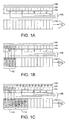
- a photosensor assembly includes a line array of photosensors 100, and a charge shift register 102.
- a charge transfer gate 104 is segmented into multiple sections. As depicted in the example of figure 1A, the charge transfer gate 104 is segmented into four equal-length sections, labeled A, B, C, and D, with each section separately controllable by control lines 106. After exposure, control of the sections of the charge transfer gate 104 determines which charges from the line array of photosensors are transferred to the charge shift register 102. For example, all four sections of the charge transfer gate 104 may be activated, so that the maximum width scanline is captured, or half the width may be captured, or any other combination of fourths.
- a lateral overflow drain 108 prevents excess charge from accumulating.
- charges in the charge shift register 102 are shifted to an amplifier 110 for analog-to-digital conversion (A/D converter not illustrated).
- processing time (which consists of shift time and A/D conversion time) is reduced to about one-fourth of the processing time required for full width scanlines.
- processing time is reduced to about one-fourth of the processing time required for full width scanline, regardless of which section of the charge transfer gate is used.
- the only variable is how many partial scanlines are multiplexed. For example, if only section A of the charge shift register is used, then processing time is reduced by about a factor of four, with no multiplexing. If only section B of the charge shift register is used, then processing time is reduced by about a factor of four, with two partial scanlines multiplexed.
- CTE Charge Transfer Efficiency
- TTE Total Transfer Efficiency
- segmented charge transfer gates With segmented charge transfer gates, fewer charges are processed during the next exposure time, so the clock rate for the charge transfer gate can be decreased, thereby improving CTE and TTE.
- both benefits may be obtained. For example, in a hypothetical scanner, assume that for full width scans the processing time for each scanline is twice the exposure time. Use of a four-segment charge transfer gate can reduce processing time by a factor of four, thereby making the exposure time twice the processing time. The shift rate can then be reduced by a factor of two, making processing time and exposure time equal, with the end result that scanning time is improved by a factor of two, and CTE and TTE are also improved.
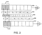
- FIG. 2 illustrates use of bilinear readout with segmented charge transfer gates in accordance with the invention.
- a line array 200 transfers charges, through a first charge transfer gate 202, to a first charge shift register 204, and through a second charge transfer gate 208, to a second charge shift register 210.
- Charge shift register 204 shifts charges to amplifier 206
- charge shift register 210 shifts charges to amplifier 212.
- charge transfer gates 202 and 210 are segmented into four equal-length sections. As depicted in figure 2, one-fourth of the charges in line array 200 are transferred to charge shift registers 204 and 210. Within each charge shift register, there is a block of charges (214, 216) that can be multiplexed with charges from successive scanlines. In the example of figure 2, if one-fourth of the charges are transferred, in the steady state after transferred charges reach the amplifiers, one-fourth of the charges in the charge shift registers are being processed while the next scanline is being exposed. Therefore, processing time is reduced to about one-fourth of the processing time required for full width scanlines. Note that in the configuration illustrated in figure 2, there is no room for lateral overflow drains adjacent to the photosensor line array. Accordingly, vertical overflow drains may be implemented beneath the photosensor line array.
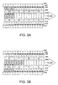
- FIG. 3A and 3B illustrate an alternative configuration, with staggered CCD arrays, in which rows of photosensors from two different staggered line arrays share a charge shift register. Sharing a charge shift register is the subject of a separate patent application. However, the configuration in figures 3A and 3B also includes segmented charge transfer gates in accordance with the invention.
- Photosensor row 300 is staggered relative to photosensor row 304.
- Two additional rows of photosensors (312 and 316) share a lateral overflow drain 314.
- Photosensor row 312 is staggered relative to photosensor row 316.
- Photosensor rows 304 and 312 share a charge shift register 308.
- Charge shift registers for photosensor rows 300 and 316 are not illustrated.
- Photosensor row 304 transfers charges, through a charge transfer gate 306, to the charge shift register 308.
- Photosensor row 312 transfers charges, through a charge transfer gate 310, to the charge shift register 308.
- charge transfer gates 306 and 310 are divided into four equal-length sections. Charges in the charge shift register 308 are shifted to an amplifier 318.
- the charge shift register 308 is used twice for each exposure.
- photosensor row 304 may transfer a block of charges to the charge shift register 308 first.
- photosensor row 312 may transfer a block of charges to the charge shift register 308.
- the charges from photosensor rows 304 and 312 may be multiplexed.
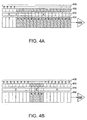
- Figures 4A and 4B illustrate example configurations in which segmented charge transfer gates have sections with unequal lengths.
- a row of photosensors 400 transfers charges, through a charge transfer gate 402, to a charge shift register 404. Excess charges from the photosensors are drained to an overflow drain 408.
- the charge transfer gate 402 is divided in two sections, labeled A and B. Section A is longer than section B.
- a specific example is a scanner capable of scanning U.S. "B" size documents or metric A3 documents, where the scanner is also routinely used to scan U.S. "A" size documents or metric A4 documents.
- section A may correspond to a partial-width scanline having a width of about 8.5 inches (U.S.
- Sections A plus B combined may correspond to a full-width scanline having a width of about 11.0 inches (U.S. size "B”), or about 297 mm (metric size A3).
- narrow documents U.S. "A” or metric A4 are placed so that resulting charges are transferred by section A of the charge transfer gate 402.
- both sections A and B of the charge transfer gate 402 are enabled.
- Figure 4B has the same overall configuration as figure 4A, except the charge transfer gate is segmented into three sections, labeled A, B, and C. Section B is smaller than sections A and C, and section B is located near the center of the overall scanline.
- a specific example is a scanner capable of scanning full width documents, but is also used to scan 35 mm slides or film negatives.
- Some light sources commonly used in optical image scanners, for example fluorescent lamps, are brighter near the center of the lamp than at the ends of the lamps. Accordingly, for such lamps, it is preferable to place slides or other small images near the center of the illumination.
- section B of the charge transfer gate 410 is located near the center of the charge transfer gate.
- processing times are compared for: (1) conventional photosensor assemblies without segmented charge transfer gates, and with normal shifting speeds; (2) rapid-shift, and (3) use of segmented charge transfer gates.
- N number of photosensors per row
- T s time to shift from one stage of the charge shift register to the next stage
- T c analog-to-digital conversion time for one voltage measurement, including some signal settling time.
- charges are transferred once in parallel, and then shifted and converted serially. Given a large number of pixels, the one charge transfer time is relatively insignificant compared to total shift time and total A/D conversion time.
- the total time required to process one scanline in conventional configurations is then approximately N*(T S + T C ). If N increases, and all other parameters remain constant, then the time required to process each scanline increases. Typically, one scanline is being exposed while the previous scan line is being converted.
- processing time is cut in half to 2.0 msec, because of the parallel charge shift registers and parallel analog-to-digital conversion.
- total processing time relative to conventional processing is cut in half to 0.875 msec.
- charge transfer gates can be divided into equal-length sections, or non-equal-length sections, with each section separately controllable.
- segmented charge transfer gates enable a decreased scanning time for small partial scanlines within longer scanlines, and improved signal accuracy (improved charge transfer efficiency).
- processing time can be reduced to 1/M times the conventional processing time.
- the location of the image within the charge shift register affects how many partial scanlines are multiplexed, but not the steady state processing time.
Landscapes
- Engineering & Computer Science (AREA)
- Multimedia (AREA)
- Signal Processing (AREA)
- Facsimile Heads (AREA)
- Solid State Image Pick-Up Elements (AREA)
- Transforming Light Signals Into Electric Signals (AREA)
- Automatic Focus Adjustment (AREA)
- Facsimile Scanning Arrangements (AREA)
Applications Claiming Priority (2)
| Application Number | Priority Date | Filing Date | Title |
|---|---|---|---|
| US09/769,721 US20020097330A1 (en) | 2001-01-25 | 2001-01-25 | Photosensor array using segmented charge transfer gates to improve processing time for small images |
| US769721 | 2001-01-25 |
Publications (1)
| Publication Number | Publication Date |
|---|---|
| EP1227664A1 true EP1227664A1 (en) | 2002-07-31 |
Family
ID=25086329
Family Applications (1)
| Application Number | Title | Priority Date | Filing Date |
|---|---|---|---|
| EP02250341A Withdrawn EP1227664A1 (en) | 2001-01-25 | 2002-01-18 | Photosensor array using segmented charge transfer gates to improve processing time for small images |
Country Status (4)
| Country | Link |
|---|---|
| US (1) | US20020097330A1 (cg-RX-API-DMAC10.html) |
| EP (1) | EP1227664A1 (cg-RX-API-DMAC10.html) |
| JP (1) | JP4045104B2 (cg-RX-API-DMAC10.html) |
| TW (1) | TW540219B (cg-RX-API-DMAC10.html) |
Cited By (1)
| Publication number | Priority date | Publication date | Assignee | Title |
|---|---|---|---|---|
| WO2007043252A1 (en) * | 2005-10-05 | 2007-04-19 | Matsushita Electric Industrial Co., Ltd. | Solid-state imaging device, imaging apparatus and driving method for the same |
Families Citing this family (5)
| Publication number | Priority date | Publication date | Assignee | Title |
|---|---|---|---|---|
| TWI220093B (en) * | 2003-07-21 | 2004-08-01 | Avision Inc | Image sensing device and its method |
| JP2008066402A (ja) * | 2006-09-05 | 2008-03-21 | Fujifilm Corp | 撮像素子および撮像装置 |
| JP2011097632A (ja) * | 2011-01-07 | 2011-05-12 | Panasonic Corp | 固体撮像装置および撮像装置 |
| FR2990299B1 (fr) * | 2012-05-03 | 2014-05-09 | E2V Semiconductors | Capteur d'image matriciel a transfert de charges bidirectionnel a grilles dissymetriques |
| US9217717B2 (en) | 2012-12-17 | 2015-12-22 | Kla-Tencor Corporation | Two dimensional optical detector with multiple shift registers |
Citations (1)
| Publication number | Priority date | Publication date | Assignee | Title |
|---|---|---|---|---|
| JPH10256522A (ja) * | 1996-07-12 | 1998-09-25 | Sony Corp | 固体撮像装置およびこれを用いたカメラ |
Family Cites Families (12)
| Publication number | Priority date | Publication date | Assignee | Title |
|---|---|---|---|---|
| US4974093A (en) * | 1987-12-22 | 1990-11-27 | Fuji Photo Film Co., Ltd. | Solid state image-pickup device with expanded dynamic range |
| US5196939A (en) * | 1989-12-28 | 1993-03-23 | Loral Fairchild Corporation | Method and apparatus for transferring images from an imaging array |
| FR2656756B1 (fr) * | 1989-12-29 | 1994-01-07 | Commissariat A Energie Atomique | Dispositif pour prises de vues a circuits de balayage integres. |
| JPH06133206A (ja) * | 1992-10-19 | 1994-05-13 | Canon Inc | 撮像装置のオートフォーカス方式 |
| US5452004A (en) * | 1993-06-17 | 1995-09-19 | Litton Systems, Inc. | Focal plane array imaging device with random access architecture |
| US5345319A (en) * | 1993-11-19 | 1994-09-06 | Goldstar Electron Co., Ltd. | Linear color charge coupled device for image sensor and method of driving the same |
| US5440343A (en) * | 1994-02-28 | 1995-08-08 | Eastman Kodak Company | Motion/still electronic image sensing apparatus |
| DE69512586T2 (de) * | 1994-08-09 | 2000-05-04 | Canon K.K., Tokio/Tokyo | Bildaufnahmevorrichtung und Bildlesegerät damit |
| US5668597A (en) * | 1994-12-30 | 1997-09-16 | Eastman Kodak Company | Electronic camera with rapid automatic focus of an image upon a progressive scan image sensor |
| JPH10108081A (ja) * | 1996-10-02 | 1998-04-24 | Sony Corp | 固体撮像装置およびその信号処理方法並びにカメラ |
| JP4019235B2 (ja) * | 1998-06-05 | 2007-12-12 | 富士フイルム株式会社 | 撮像デバイスの駆動方法及び電子カメラ |
| US6459077B1 (en) * | 1998-09-15 | 2002-10-01 | Dalsa, Inc. | Bucket brigade TDI photodiode sensor |
-
2001
- 2001-01-25 US US09/769,721 patent/US20020097330A1/en not_active Abandoned
- 2001-07-26 TW TW090118301A patent/TW540219B/zh not_active IP Right Cessation
-
2002
- 2002-01-18 EP EP02250341A patent/EP1227664A1/en not_active Withdrawn
- 2002-01-23 JP JP2002013958A patent/JP4045104B2/ja not_active Expired - Fee Related
Patent Citations (1)
| Publication number | Priority date | Publication date | Assignee | Title |
|---|---|---|---|---|
| JPH10256522A (ja) * | 1996-07-12 | 1998-09-25 | Sony Corp | 固体撮像装置およびこれを用いたカメラ |
Non-Patent Citations (1)
| Title |
|---|
| PATENT ABSTRACTS OF JAPAN vol. 1998, no. 14 31 December 1998 (1998-12-31) * |
Cited By (3)
| Publication number | Priority date | Publication date | Assignee | Title |
|---|---|---|---|---|
| WO2007043252A1 (en) * | 2005-10-05 | 2007-04-19 | Matsushita Electric Industrial Co., Ltd. | Solid-state imaging device, imaging apparatus and driving method for the same |
| US8102450B2 (en) | 2005-10-05 | 2012-01-24 | Panasonic Corporation | Solid-state imaging device, imaging apparatus and driving method for the same |
| US8319876B2 (en) | 2005-10-05 | 2012-11-27 | Panasonic Corporation | Solid-state imaging device, imaging apparatus and driving method for the same |
Also Published As
| Publication number | Publication date |
|---|---|
| US20020097330A1 (en) | 2002-07-25 |
| JP2002320069A (ja) | 2002-10-31 |
| JP4045104B2 (ja) | 2008-02-13 |
| TW540219B (en) | 2003-07-01 |
Similar Documents
| Publication | Publication Date | Title |
|---|---|---|
| US6894812B1 (en) | Photosensor assembly with shared structures | |
| JP4041695B2 (ja) | 空間分解能が異なる複数のリニアフォトセンサアレイを備える影像装置 | |
| JP2004112611A (ja) | 画像読取装置 | |
| US20020097330A1 (en) | Photosensor array using segmented charge transfer gates to improve processing time for small images | |
| US5995249A (en) | Image sensing device and image reading apparatus using the same that reduces the influence of color mixture due to intrapixel transfer | |
| US6900427B2 (en) | Photosensor assembly with shared charge transfer registers and electronic shutters | |
| US4754153A (en) | Operating radiation sensors to avoid transfer loss | |
| JPH1132166A (ja) | イメージセンサと画像読み取り装置 | |
| US6765699B1 (en) | Photosensor array with decreased scan time for decreased optical sampling rates | |
| EP1150498B1 (en) | Photosensor array using multiple exposures to reduce thermal noise | |
| JP3259975B2 (ja) | 画像読取装置 | |
| JP2000101805A (ja) | 原画の走査装置 | |
| US20040212857A1 (en) | Control for a photosensor array | |
| US7538913B2 (en) | Stagger sensor and method for improving modulation transfer function | |
| US6700682B1 (en) | Image processing system capable of easily changing subscanning magnification in image read | |
| JPH05207232A (ja) | 画像読取装置 | |
| JP3229347B2 (ja) | 画像読取装置 | |
| JPH0946489A (ja) | 画像読み取り装置 | |
| JPH05300309A (ja) | 画像読み取り装置および方法 | |
| JP2000022904A (ja) | 画像読取装置及び画像読取方法 | |
| JP2002118717A (ja) | 分割1次元固体撮像素子、その制御方法およびこれを用いる画像読取装置 | |
| GB2383899A (en) | Photosensor assembly with staggered line arrays of sensors | |
| JPH07162621A (ja) | 画情報の読み取り装置 |
Legal Events
| Date | Code | Title | Description |
|---|---|---|---|
| PUAI | Public reference made under article 153(3) epc to a published international application that has entered the european phase |
Free format text: ORIGINAL CODE: 0009012 |
|
| AK | Designated contracting states |
Kind code of ref document: A1 Designated state(s): AT BE CH CY DE DK ES FI FR GB GR IE IT LI LU MC NL PT SE TR |
|
| AX | Request for extension of the european patent |
Free format text: AL;LT;LV;MK;RO;SI |
|
| 17P | Request for examination filed |
Effective date: 20020927 |
|
| AKX | Designation fees paid |
Designated state(s): DE FR GB NL |
|
| 17Q | First examination report despatched |
Effective date: 20041119 |
|
| GRAP | Despatch of communication of intention to grant a patent |
Free format text: ORIGINAL CODE: EPIDOSNIGR1 |
|
| RIC1 | Information provided on ipc code assigned before grant |
Ipc: H04N 5/369 20110101AFI20110113BHEP Ipc: H04N 5/345 20110101ALI20110113BHEP Ipc: H04N 5/372 20110101ALI20110113BHEP |
|
| STAA | Information on the status of an ep patent application or granted ep patent |
Free format text: STATUS: THE APPLICATION IS DEEMED TO BE WITHDRAWN |
|
| 18D | Application deemed to be withdrawn |
Effective date: 20110618 |