EP1223604A1 - Flüssigkristallanzeigevorrichtung, optisch anisotroper film, und deren herstellungsmethoden - Google Patents
Flüssigkristallanzeigevorrichtung, optisch anisotroper film, und deren herstellungsmethoden Download PDFInfo
- Publication number
- EP1223604A1 EP1223604A1 EP00966348A EP00966348A EP1223604A1 EP 1223604 A1 EP1223604 A1 EP 1223604A1 EP 00966348 A EP00966348 A EP 00966348A EP 00966348 A EP00966348 A EP 00966348A EP 1223604 A1 EP1223604 A1 EP 1223604A1
- Authority
- EP
- European Patent Office
- Prior art keywords
- liquid crystal
- orientation
- substrates
- regions
- molecules
- Prior art date
- Legal status (The legal status is an assumption and is not a legal conclusion. Google has not performed a legal analysis and makes no representation as to the accuracy of the status listed.)
- Withdrawn
Links
Images


Classifications
-
- G—PHYSICS
- G02—OPTICS
- G02F—OPTICAL DEVICES OR ARRANGEMENTS FOR THE CONTROL OF LIGHT BY MODIFICATION OF THE OPTICAL PROPERTIES OF THE MEDIA OF THE ELEMENTS INVOLVED THEREIN; NON-LINEAR OPTICS; FREQUENCY-CHANGING OF LIGHT; OPTICAL LOGIC ELEMENTS; OPTICAL ANALOGUE/DIGITAL CONVERTERS
- G02F1/00—Devices or arrangements for the control of the intensity, colour, phase, polarisation or direction of light arriving from an independent light source, e.g. switching, gating or modulating; Non-linear optics
- G02F1/01—Devices or arrangements for the control of the intensity, colour, phase, polarisation or direction of light arriving from an independent light source, e.g. switching, gating or modulating; Non-linear optics for the control of the intensity, phase, polarisation or colour
- G02F1/13—Devices or arrangements for the control of the intensity, colour, phase, polarisation or direction of light arriving from an independent light source, e.g. switching, gating or modulating; Non-linear optics for the control of the intensity, phase, polarisation or colour based on liquid crystals, e.g. single liquid crystal display cells
- G02F1/133—Constructional arrangements; Operation of liquid crystal cells; Circuit arrangements
- G02F1/1333—Constructional arrangements; Manufacturing methods
- G02F1/1337—Surface-induced orientation of the liquid crystal molecules, e.g. by alignment layers
- G02F1/13378—Surface-induced orientation of the liquid crystal molecules, e.g. by alignment layers by treatment of the surface, e.g. embossing, rubbing or light irradiation
- G02F1/133788—Surface-induced orientation of the liquid crystal molecules, e.g. by alignment layers by treatment of the surface, e.g. embossing, rubbing or light irradiation by light irradiation, e.g. linearly polarised light photo-polymerisation
-
- G—PHYSICS
- G02—OPTICS
- G02F—OPTICAL DEVICES OR ARRANGEMENTS FOR THE CONTROL OF LIGHT BY MODIFICATION OF THE OPTICAL PROPERTIES OF THE MEDIA OF THE ELEMENTS INVOLVED THEREIN; NON-LINEAR OPTICS; FREQUENCY-CHANGING OF LIGHT; OPTICAL LOGIC ELEMENTS; OPTICAL ANALOGUE/DIGITAL CONVERTERS
- G02F1/00—Devices or arrangements for the control of the intensity, colour, phase, polarisation or direction of light arriving from an independent light source, e.g. switching, gating or modulating; Non-linear optics
- G02F1/01—Devices or arrangements for the control of the intensity, colour, phase, polarisation or direction of light arriving from an independent light source, e.g. switching, gating or modulating; Non-linear optics for the control of the intensity, phase, polarisation or colour
- G02F1/13—Devices or arrangements for the control of the intensity, colour, phase, polarisation or direction of light arriving from an independent light source, e.g. switching, gating or modulating; Non-linear optics for the control of the intensity, phase, polarisation or colour based on liquid crystals, e.g. single liquid crystal display cells
- G02F1/133—Constructional arrangements; Operation of liquid crystal cells; Circuit arrangements
- G02F1/1333—Constructional arrangements; Manufacturing methods
- G02F1/1337—Surface-induced orientation of the liquid crystal molecules, e.g. by alignment layers
- G02F1/133711—Surface-induced orientation of the liquid crystal molecules, e.g. by alignment layers by organic films, e.g. polymeric films
- G02F1/133719—Surface-induced orientation of the liquid crystal molecules, e.g. by alignment layers by organic films, e.g. polymeric films with coupling agent molecules, e.g. silane
-
- G—PHYSICS
- G02—OPTICS
- G02F—OPTICAL DEVICES OR ARRANGEMENTS FOR THE CONTROL OF LIGHT BY MODIFICATION OF THE OPTICAL PROPERTIES OF THE MEDIA OF THE ELEMENTS INVOLVED THEREIN; NON-LINEAR OPTICS; FREQUENCY-CHANGING OF LIGHT; OPTICAL LOGIC ELEMENTS; OPTICAL ANALOGUE/DIGITAL CONVERTERS
- G02F1/00—Devices or arrangements for the control of the intensity, colour, phase, polarisation or direction of light arriving from an independent light source, e.g. switching, gating or modulating; Non-linear optics
- G02F1/01—Devices or arrangements for the control of the intensity, colour, phase, polarisation or direction of light arriving from an independent light source, e.g. switching, gating or modulating; Non-linear optics for the control of the intensity, phase, polarisation or colour
- G02F1/13—Devices or arrangements for the control of the intensity, colour, phase, polarisation or direction of light arriving from an independent light source, e.g. switching, gating or modulating; Non-linear optics for the control of the intensity, phase, polarisation or colour based on liquid crystals, e.g. single liquid crystal display cells
- G02F1/133—Constructional arrangements; Operation of liquid crystal cells; Circuit arrangements
- G02F1/1333—Constructional arrangements; Manufacturing methods
- G02F1/1337—Surface-induced orientation of the liquid crystal molecules, e.g. by alignment layers
- G02F1/133753—Surface-induced orientation of the liquid crystal molecules, e.g. by alignment layers with different alignment orientations or pretilt angles on a same surface, e.g. for grey scale or improved viewing angle
- G02F1/133761—Surface-induced orientation of the liquid crystal molecules, e.g. by alignment layers with different alignment orientations or pretilt angles on a same surface, e.g. for grey scale or improved viewing angle with different pretilt angles
-
- G—PHYSICS
- G02—OPTICS
- G02F—OPTICAL DEVICES OR ARRANGEMENTS FOR THE CONTROL OF LIGHT BY MODIFICATION OF THE OPTICAL PROPERTIES OF THE MEDIA OF THE ELEMENTS INVOLVED THEREIN; NON-LINEAR OPTICS; FREQUENCY-CHANGING OF LIGHT; OPTICAL LOGIC ELEMENTS; OPTICAL ANALOGUE/DIGITAL CONVERTERS
- G02F1/00—Devices or arrangements for the control of the intensity, colour, phase, polarisation or direction of light arriving from an independent light source, e.g. switching, gating or modulating; Non-linear optics
- G02F1/01—Devices or arrangements for the control of the intensity, colour, phase, polarisation or direction of light arriving from an independent light source, e.g. switching, gating or modulating; Non-linear optics for the control of the intensity, phase, polarisation or colour
- G02F1/13—Devices or arrangements for the control of the intensity, colour, phase, polarisation or direction of light arriving from an independent light source, e.g. switching, gating or modulating; Non-linear optics for the control of the intensity, phase, polarisation or colour based on liquid crystals, e.g. single liquid crystal display cells
- G02F1/133—Constructional arrangements; Operation of liquid crystal cells; Circuit arrangements
- G02F1/1333—Constructional arrangements; Manufacturing methods
- G02F1/1343—Electrodes
- G02F1/134309—Electrodes characterised by their geometrical arrangement
- G02F1/134363—Electrodes characterised by their geometrical arrangement for applying an electric field parallel to the substrate, i.e. in-plane switching [IPS]
Definitions
- the present invention relates to a liquid crystal display element and a method of producing the same and to an optically anisotropic film and a method of producing the same, the aforesaid for a liquid crystal display panel used in a flat panel display that displays, for example, TV or computer images.
- TN mode liquid crystal display element that uses a liquid crystal having a positive dielectric anisotropy, for example, has been put into practical use.
- This TN mode LCD is driven by applying an electric field in a direction perpendicular to the substrate surfaces to change the orientation of the liquid crystal molecules such that their long axes are parallel to the direction of the electric field.
- the polar anchoring energy of all regions of the pixels has been increased.
- the influence of the transverse electric field in pixel regions other than the perimeter portions is small, and when the polar anchoring energy is large in these regions, coloration arises.
- Transverse electric field-driven liquid crystal display elements provided with counter electrodes on a substrate surface have also been developed.
- in-plane switching (IPS) mode LCDs which switch the liquid crystal molecules in a direction within the plane of the substrates by applying a so-called transverse electric field in a direction parallel to the substrate surfaces.
- IPS mode LCDs In the area above the electrodes in IPS mode LCDs, a transverse electric field is not generated, but rather an electric field is generated in a direction perpendicular to the substrate surfaces. For this reason, the alignment state of liquid crystal above the electrodes cannot be changed.
- the liquid crystal layer comes to have both a region in which molecules transition to a new alignment state and a region in which molecules remain in the initial orientation state.
- IPS mode LCDs are disadvantageous in that response speed is even slower than that of conventional vertical electric field mode LCDs.
- orientation films having the same anchoring energy are provided on opposing substrates.
- liquid crystal molecules above the substrate having electrodes on its surface rotate to at most approximately 90° when driving is ON.
- liquid crystal molecules above the substrate without electrodes on its surface hardly rotate.
- liquid crystal display elements operated in twisted nematic (TN) mode which use a liquid crystal having a positive dielectric anisotropy
- those operated in IPS mode which have a very wide viewing angle and whose the liquid crystal molecules are driven within a plane using transverse electric field, and the like have been put into practical use.
- a bend alignment-type liquid crystal display element which utilizes a change in refractive index caused by the change in the rise angle of each liquid crystal molecule in a state wherein the liquid crystal molecules between the substrates show a bend alignment (OCB mode liquid crystal display element).
- OBC mode liquid crystal display element In comparison to the speed of the change in alignment between an ON state and an OFF state in a TN liquid crystal display element, the speed of change in alignment of each of liquid crystal molecules showing a bend alignment between an ON state and an OFF state is very high speed, making it possible to obtain a liquid crystal display element that is excellent in terms of response.
- the bend alignment-type liquid crystal display element described above is self-compensating in terms of optical retardation because all of the liquid crystal molecules between the upper and lower substrates show bend alignment, and the display element enables a wide viewing angle at low-voltage operation by the provision of a film retardation plate that compensates for retardation.
- the liquid crystal display element described above is usually fabricated so that the liquid crystal of the liquid crystal layer shows a splay alignment when voltage is not being applied. Therefore, in order to utilize the bend alignment to change the refractive index, it is necessary to uniformly transition the entire display portion from a splay alignment state to a bend alignment state.
- the transition to a bend alignment proceeds with transition seeds as the center.
- the location of transition seed generation is not regular, appearing, for example, at orientation irregularities or damaged areas of the orientation film interface. Because the location of transition seed generation is not fixed, display defects tend to arise. Therefore, it is very important to uniformly transition the entire display portion from a splay alignment to a bend alignment before use.
- the perimeter portion of the display region of a liquid crystal display element does not contribute to liquid crystal display. Thus, it is not necessary to inject liquid crystal into the perimeter portion of the display region.
- liquid crystal injected into the perimeter portion of the display region is wasted, as it is difficult to inject the liquid crystal without also injecting the liquid crystal into the perimeter portion of the display region.
- orientation films having more than one liquid crystal orientation has been proposed in order to improve the display characteristics of liquid crystal display elements.
- further improvement in display characteristics is needed beyond what has been realized by such methods.
- the first invention group provides a liquid crystal display element comprising a liquid crystal sandwiched between two opposed substrates each having an orientation film, wherein the two orientation films comprise molecules having a photosensitive group and have different orientation anisotropies from one another, the molecules having been irradiated with polarized light, and wherein a pretilt angle of liquid crystal molecules corresponding to the orientation anisotropy of the orientation film provided on an inner side of one of the opposed substrates differs from a pretilt angle of liquid crystal molecules corresponding to the orientation anisotropy of the orientation film provided on an inner side of the other opposed substrate.
- This construction makes is possible, by irradiating orientation films of a liquid crystal display element with polarized ultraviolet light, to easily provide orientation films that can induce a pretilt angle in liquid crystal molecules for various modes of the liquid crystal display.
- the polarized light irradiation may be such that the molecules having photosensitive groups, for example, are irradiated with polarized light of different irradiation intensity.
- the molecules may also be irradiated with polarized light applied at different angles to the substrates.
- one of the opposed substrates may have opposed electrodes on a surface thereof, and the pretilt angle of the liquid crystal molecules corresponding to the orientation anisotropy of the orientation film provided on the inner side of the one opposed substrate may be greater than the pretilt angle of the liquid crystal molecules corresponding to the orientation anisotropy of the orientation film provided on the inner side of the other opposed substrate.
- an electric field above the electrodes orients liquid crystal molecules to a specified pretilt angle when driving is ON in, for example, an IPS mode liquid crystal display element.
- Response speed is thus improved by orienting liquid crystal molecules above the substrate having the electrodes to somewhat of a pretilt angle even when driving is OFF.
- the liquid crystal display elements described above may be produced by, for example, forming thin films on a pair of substrates using molecules having at least a photosensitive group; carrying out an orientation treatment by irradiating one of the thin films and the other of the thin films with polarized light under different irradiation conditions so that the orientation anisotropy of the one thin film and that of the other thin film are made different; forming a sealing material on either of the substrates in a frame shape excluding a portion for a liquid crystal injection port; and adhering the substrates together.
- This construction makes it possible to simply obtain orientation films that induce different pretilt angles by irradiating the one of the thin films and the other of the thin films with polarized light under different irradiation conditions.
- the irradiation be such that the one of the thin films and the other of the thin films are irradiated with polarized light of different irradiation intensity.
- the irradiation be such that the one of the thin films and the other of the thin films are irradiated with polarized light having parallel planes of polarization and different angles of incidence with respect to surfaces of the substrates.
- one of the opposed substrates may have opposed electrodes on a surface thereof, and the orientation treatment may be carried out under orientation conditions such that a pretilt angle of liquid crystal molecules corresponding to the orientation anisotropy of an orientation film provided on an inner side of the one opposed substrate is made greater than a pretilt angle of liquid crystal molecules corresponding to the orientation anisotropy of an orientation film provided on an inner side of the other opposed substrate.
- the second invention group provides a liquid crystal display element capable of hybrid liquid crystal orientation.
- a liquid crystal display element comprising a liquid crystal sandwiched between two opposed substrates each having an orientation film, wherein at least one of the orientation films comprises molecules having a photosensitive group and has at least two regions with different orientation anisotropies, the molecules having been irradiated with polarized light, and wherein liquid crystal molecules have pretilt angles such as to correspond to the orientation anisotropies of the regions of the orientation film.
- This construction makes it possible to control the pretilt angle to a pretilt angle that can be consistently reproduced, as pretilt angle is controlled by the irradiation of polarized light. Because the at least two regions having different orientation anisotropy are provided by irradiation with polarized light, the production process is simplified and contamination and the like of the orientation film by a protective film is not a problem in comparison with rubbing treatment.
- each region be provided by irradiation of the molecules having a photosensitive group with polarized light of differing irradiation intensities.
- the at least two regions having different orientation anisotropies be provided by irradiation with polarized light applied at differing angles to the substrates.
- orientation films should be provided with at least two regions having different orientation anisotropies
- an orientation film provided with at least two regions having different orientation anisotropies be provided on an inner side of each of the opposed substrates such that regions of the orientation films having a same orientation are opposed to one another.
- This construction makes is possible to provide a liquid crystal display element excellent in terms of liquid crystal orientation.
- liquid crystal display elements described above may be produced by, for example, the following methods.
- the liquid crystal display elements may be produced by forming thin films on a pair of substrates using molecules having at least a photosensitive group; carrying out an orientation treatment by irradiating different areas of at least one of the thin films with polarized light under different irradiation conditions to form at least two regions having different orientation anisotropies on the at least one of the thin films; forming a sealing material on either of the substrates in a frame shape excluding a portion for a liquid crystal injection port; adhering the substrates together; and injecting a liquid crystal between the substrates through the liquid crystal injection port to form a liquid crystal layer.
- This construction makes it possible to simply produce, for various liquid crystal display modes of liquid crystal display elements, orientation films having a plurality of orientation anisotropies by using a shadow mask on the thin films on the surfaces of the substrates.
- the irradiation be such that different areas of at least one of the thin films be irradiated with polarized light of different irradiation intensity.
- the irradiation be such that different areas of at least one of the thin films be irradiated with polarized light having parallel planes of polarization and different angles of incidence with respect to surfaces of the substrates.
- invention group 2-1 provides a TN mode liquid crystal display device for preventing the generation of disclination by transverse electric fields and for suppressing a deterioration in contrast and the like that is caused by this disclination.
- the present invention provides a liquid crystal display element, wherein the liquid crystal display element is a twisted nematic orientation mode liquid crystal display element comprising a liquid crystal layer with an initial orientation state in twisted orientation mode provided between a pair of substrates; and a transverse electric field suppressing region in which liquid crystal molecules have been oriented at a higher pretilt angle than are liquid crystal molecules in an inner region of each pixel region is provided in a perimeter portion of each pixel region in the liquid crystal layer.
- the liquid crystal display element is a twisted nematic orientation mode liquid crystal display element comprising a liquid crystal layer with an initial orientation state in twisted orientation mode provided between a pair of substrates; and a transverse electric field suppressing region in which liquid crystal molecules have been oriented at a higher pretilt angle than are liquid crystal molecules in an inner region of each pixel region is provided in a perimeter portion of each pixel region in the liquid crystal layer.
- transverse electric field disclination In a conventional TN mode liquid crystal display element, orientation abnormalities such as disclination arise due to the influence of a transverse electric field in the perimeter portion of each pixel region, and this is a cause of the generation of disclination at boundaries between the perimeter portions and portions of the pixel regions other than the perimeter portions.
- Generation of disclination such as this caused by a transverse electric field invites deterioration in contrast and thus is a cause of degradation in display characteristics.
- each pixel region is divided into a perimeter portion that is influenced by a transverse electric field and an inner region that is not, and a transverse electric field suppressing region is provided in each perimeter portion such that liquid crystal molecules are oriented at a higher pretilt angle in the perimeter portions than in the inner regions.
- a transverse electric field suppressing region is provided in each perimeter portion such that liquid crystal molecules are oriented at a higher pretilt angle in the perimeter portions than in the inner regions.
- the construction described above be such that an orientation film for orienting liquid crystal molecules in a specified direction be provided on an inner side of each of the substrates; and the orientation film comprise a high pretilt angle region for initially orienting liquid crystal molecules at a high pretilt angle in each of the transverse electric field suppressing regions and a low pretilt angle region for initially orienting liquid crystal molecules at a low pretilt angle in each of the inner regions.
- the orientation film at least contain thin film components each having a photosensitive group, the photosensitive groups being polymerized and fixed in a desired direction.
- the orientation film be a thin film formed of a group of molecules including at least molecules of a silane-based compound each having a photosensitive group, the group of molecules being bonded and fixed to each of the substrates.
- the group of molecules be inclined in a specified direction and the photosensitive groups polymerized and fixed in the specified direction.
- the orientation film be a monomolecular film.
- the present invention provides a method of producing a liquid crystal display element that is a twisted nematic orientation mode liquid crystal display element having a liquid crystal layer with an initial orientation state in twisted orientation mode provided between a pair of substrates, the method comprising the steps of forming orientation films on the pair of substrates; carrying out an orientation treatment on each of the orientation films such that orientation treatment conditions for regions of the liquid crystal layer corresponding to perimeter portions of pixel regions are made different from orientation treatment conditions for regions corresponding to inner regions, which are regions other than the perimeter portions, to form high pretilt angle regions for orienting liquid crystal molecules at a high pretilt angle in the regions corresponding to the perimeter portions and low pretilt angle regions for orienting liquid crystal molecules at a low pretilt angle in the regions corresponding to the inner regions; adhering the substrates together; and injecting a liquid crystal between the substrates through an injection port to form a liquid crystal layer; whereby transverse electric field suppressing regions are formed in the perimeter portions of the pixel regions in the liquid crystal layer, the transverse
- the method described above makes it possible to provide a liquid crystal display element for suppressing generation of reverse tilt even with influence from a transverse electric field by carrying out an orientation treatment on the orientation films formed on the substrates to form a high pretilt angle region for orienting liquid crystal molecules at a high pretilt angle in each region corresponding to the perimeter portion of each pixel region.
- a liquid crystal display element for suppressing generation of reverse tilt even with influence from a transverse electric field by carrying out an orientation treatment on the orientation films formed on the substrates to form a high pretilt angle region for orienting liquid crystal molecules at a high pretilt angle in each region corresponding to the perimeter portion of each pixel region.
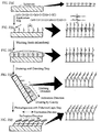
- the step of carrying out an orientation treatment be a step of carrying out an orientation treatment by polarized photoalignment such that surfaces of the substrates having the orientation films formed thereon are irradiated with polarized light; and that the irradiation with polarized light be carried out such that the irradiation intensity of a first polarized light applied to the perimeter portions of the pixel regions is made greater than the irradiation intensity of a second polarized light applied to the regions of the pixel regions other than the perimeter portions.
- the step of carrying out an orientation treatment be a step of carrying out an orientation treatment by polarized photoalignment such that surfaces of the substrates having the orientation films formed thereon are irradiated with polarized light; and that the irradiation with polarized light is carried out such that the plane of polarization of a first polarized light applied to the formation regions and a second plane of polarization applied to the formation regions are made parallel, and the angle of incidence with respect to the substrate surfaces of the first polarized light is made smaller than the angle of incidence with respect to the substrate surfaces of the second polarized light.
- the step of forming orientation films be such that a silane-based compound having photosensitive groups is contacted to the substrate surfaces under a dry atmosphere, whereby the silane-based compound is chemisorbed to the substrate surfaces.
- invention group 2-2 provides an IPS mode liquid crystal display element having good response speed by making it possible to sufficiently drive liquid crystal above the electrodes.
- the present invention provides an in-plane switching-type liquid crystal display element having a liquid crystal layer provided between a pair of substrates and pairs of electrodes provided on one of the substrates, the display element wherein: the liquid crystal layer comprises, first regions provided above the electrodes, wherein liquid crystal alignment is controlled by electric field components above the electrodes; and a second region corresponding to an area between the pairs of electrodes, wherein liquid crystal alignment is controlled by transverse electric field components; wherein a pretilt angle of liquid crystal molecules in the first regions is larger than a pretilt angle of liquid crystal molecules in the second region.
- an orientation film for orienting liquid crystal molecules in a substantially same direction be provided on an inner side of one of the substrates, the orientation film having high pretilt angle regions for initially orienting liquid crystal molecules above the pairs of electrodes at a high pretilt angle and a low pretilt angle region for initially orienting liquid crystal molecules between the pairs of electrodes at a low pretilt angle.
- orientation film control the orientation of liquid crystal molecules such that pretilt angle increases continuously and progressively toward the electrodes.
- each of the pairs of electrodes be a transparent electrode.
- the orientation film at least contain thin film component molecules each having a photosensitive group, the photosensitive groups being polymerized and fixed in a desired direction.
- the orientation film be a thin film formed of a group of molecules including at least molecules of a silane-based compound each having a photosensitive group, the group of molecules being bonded and fixed on each of the substrates.
- the group of molecules be inclined in a specified direction and that the photosensitive groups be polymerized and fixed in the specified direction.
- the orientation film be a monomolecular film.
- the present invention provides a method of producing a liquid crystal display element that is an in-plane switching-type liquid crystal display element provided with a liquid crystal layer between a pair of substrates and pairs of electrodes on one of the substrates, the method comprising the steps of: forming orientation films on the pair of substrates; carrying out an orientation treatment on the orientation films such that orientation treatment conditions for regions above the pairs of electrodes are made different from orientation treatment conditions for regions corresponding to an area between the pairs of electrodes to form high pretilt angle regions for orienting liquid crystal molecules at a high pretilt angle in the regions above the pairs of electrodes and a low pretilt angle region for orienting liquid crystal molecules at a low pretilt angle in the region corresponding to the area between the pairs of electrodes; adhering the substrates together; and injecting a liquid crystal between the substrates to form a liquid crystal layer; whereby in the liquid crystal layer, first regions and a second region are formed, the first regions provided above the electrodes, wherein
- the step of carrying out an orientation treatment be a step of carrying out an orientation treatment such that surfaces of the substrates having the orientation films formed thereon are irradiated with polarized light; and the irradiation with polarized light be carried out such that the irradiation intensity of a first polarized light applied to the regions above the pairs of electrodes is made greater than the irradiation intensity of a second polarized light applied to the region corresponding to the area between the pairs of electrodes.
- the step of carrying out an orientation treatment be a step of carrying out an orientation treatment by photoalignment with polarized light such that surfaces of the substrates having the orientation films formed thereon are irradiated with polarized light; and the irradiation with polarized light be carried out such that the plane of polarization of a first polarized light applied above the pairs of electrodes and a second plane of polarization applied to the region corresponding to the area between the electrodes are made parallel, and the angle of incidence with respect to the substrate surfaces of the first polarized light is made smaller than the angle of incidence with respect to the substrate surfaces of the second polarized light.
- the step of forming orientation films be such that a silane-based compound having photosensitive groups is contacted to the substrate surfaces under a dry atmosphere, whereby the silane-based compound is chemisorbed to the substrate surfaces.
- liquid crystal layer comes to have both regions in which the liquid crystal transitions to a new alignment state and regions in which the liquid crystal remains in the initial orientation state, whereby at least in the boundary portions between both regions, continuity in the alignment state of the liquid crystal (during application of an electric field) is not maintained, factoring into a deterioration of response.
- the creation of the first regions is achieved by initially orienting liquid crystal molecules in the first regions to a larger pretilt angle than that to which liquid crystal molecules in the second region are oriented.
- the liquid crystal molecules are initially oriented to a high pretilt angle, the long axis direction and the like of the liquid crystal molecules can be easily lined up with the vertical electric field direction.
- an orientation film having high pretilt angle regions above the pairs of electrodes and a low pretilt angle region between the pairs of electrodes, it is possible to initially orient liquid crystal molecules in the first regions to a high pretilt angle and liquid crystal molecules in the second region to a low pretilt angle.
- the region of liquid crystal that can be operated is enlarged.
- the electrode formation regions also contribute to screen display, thereby improving light usage efficiency. As a result, a much brighter display can be achieved.
- the orientation state of liquid crystal molecules in the formation regions can be changed by electric field components above the electrodes. Even when an electric field is being applied, continuity in liquid crystal state is maintained at the boundary portions between the first regions and the second region, making it possible to realize a smooth transition between liquid crystal alignment states and to thereby produce a liquid crystal display element having excellent response.
- the present invention provides a liquid crystal display element comprising a liquid crystal layer oriented in splay alignment provided between a pair of substrates with electrodes, each substrate having an orientation film, the display element wherein: at least one of the orientation films comprises thin film component molecules each having a photosensitive group and high pretilt regions for orienting liquid crystal molecules to a higher pretilt angle than do other regions; and the liquid crystal layer has transition seed generation regions wherein a transition from splay alignment to bend alignment is accelerated by application of a voltage to the electrodes, the transition seed generation regions being formed by the high pretilt angle regions.
- At least one of the transition seed generation regions be provided in each pixel region in the liquid crystal layer.
- the construction described above be such that the one orientation film be a thin film formed of a group of silane-based compound each having a photosensitive group, the group being bonded and fixed on one of the substrates.
- the silane-based compound molecules comprise a linear hydrocarbon chain.
- the silane-based compound molecules can be well aligned on the substrate, making it possible to form a highly dense, chemisorbed thin film.
- a liquid crystal display element having an orientation film with excellent orientation properties can be obtained.
- the construction be such that a photosensitive group portion in the thin film component molecules is polymerized and fixed in a desired direction.
- the orientation film be a monomolecular film.
- the photosensitive group portion be cinnamoyl groups or chalconyl groups.
- the present invention provides a method of producing a liquid crystal display element having a liquid crystal layer oriented in splay alignment provided between a pair of substrates with electrodes, each substrate having an orientation film, the method comprising the steps of: forming an orientation film comprising thin film components each having a photosensitive group on at least one of the substrates; carrying out an orientation treatment that utilizes a photoalignment method on the orientation film wherein irradiation conditions are varied to form high pretilt angle regions for orienting liquid crystal molecules at a higher pretilt angle than do other regions; adhering the substrates together; and injecting a liquid crystal between the substrates to form a liquid crystal layer; whereby transition seed generation regions for accelerating a transition from splay alignment to bend alignment with application of a voltage to the electrodes are provided in the liquid crystal layer, the transition seed generation regions being formed by the high pretilt angle regions.
- the step of carrying out an orientation treatment be such that polarized light having a greater irradiation intensity than polarized light applied to the other regions is applied to specified regions to form the high pretilt angle regions in the specified regions.
- the step of carrying out an orientation treatment be such that polarized light having a smaller angle of incidence than polarized light applied to the other regions is applied to specified regions to form the high pretilt angle regions in the specified regions.
- the step of carrying out an orientation treatment be such that a silane-based compound having photosensitive groups is contacted to the substrate surface under a dry atmosphere, whereby the silane-based compound is chemisorbed to the substrate surface.
- a liquid crystal display element in accordance with the present invention is such that transition seed generation regions are provided in the liquid crystal layer by forming high pretilt angle regions for orienting liquid crystal molecules to a higher pretilt angle than to other regions in the orientation film. Orienting liquid crystal molecules to a higher pretilt angle than to other regions makes it possible to provide a liquid crystal alignment state having a distorted construction in these regions.
- liquid crystal molecules in these regions rise (transition) quickly as compared to liquid crystal molecules of other regions, whereby transitions seeds are generated.
- the generation of transition seeds accelerates a transition from splay alignment to bend alignment, thereby reducing the splay-bend transition voltage.
- the orientation film be a thin film formed of a group of thin film components each having a photosensitive group and bonded to a substrate, a photosensitive group of the thin film components being polymerized and fixed in a specified direction.
- the orientation of liquid crystal molecules can be controlled in the direction in which the photosensitive group is polymerized and fixed, making it possible to obtain a liquid crystal display element having excellent orientation uniformity.
- orientation treatment on the orientation film is carried out using a photoalignment method (polarized photoalignment step), eliminating the need to form a photoresist (protective film) by photolithography as was necessary in carrying out of the conventional rubbing treatment.
- a photoalignment method polarized photoalignment step
- the generation of dust does not arise with the photoalignment method, making it possible to prevent contamination of the orientation film.
- high pretilt angle regions can be formed in the specified regions with good reproducibility.
- high pretilt angle regions can be formed in the specified regions by irradiating these regions with polarized light applied at an incidence angle that is larger than that of polarized light applied to other regions.
- the third invention group provides a liquid crystal display element having excellent display characteristics by providing an orientation film on each of a pair of substrates in a liquid crystal display element and making the anchoring energy, with respect to liquid crystal molecules, of each respective orientation film different.
- the present invention provides a liquid crystal display element comprising a liquid crystal sandwiched between two opposed substrates each having an orientation film, wherein the two orientation films comprise molecules having a photosensitive group and have different orientation anisotropies from one another, the molecules having been irradiated with polarized light, and wherein an anchoring energy, with respect to liquid crystal molecules, of the orientation film provided on an inner side of one of the opposed substrates differs from an anchoring energy, with respect to liquid crystal molecules, of the orientation film provided on an inner side of the other opposed substrate.
- each display element provided with orientation films that have an anchoring energy with respect to liquid crystal molecules.
- the anchoring energy with respect to liquid crystal molecules can be made large.
- the anchoring energy with respect to liquid crystal molecules can be made small because it is not necessary that the anchoring energy with respect to the liquid crystal molecules be a particularly large azimuthal anchoring energy.
- the controlling of the anchoring energy can be realized with good reproducibility.
- Such a liquid crystal display element of the present invention may also be obtained by employing the two orientation films comprising molecules having a photosensitive group, the molecules having been irradiated with polarized light of different irradiation intensity.
- Such a liquid crystal display element of the present invention may also be obtained by employing the two orientation films comprising molecules having a photosensitive group, the molecules having been irradiated with polarized light applied at different angles to the substrates.
- the molecules having a photosensitive group be molecules of a silane-based compound, a group of the molecules forming a thin film bonded and fixed to each of the substrates.
- Opposed electrodes may be provided on one of the substrates.
- the anchoring energy, with respect to liquid crystal molecules, of the orientation film provided on an inner side of one of the opposed substrates be greater than the anchoring energy, with respect to liquid crystal molecules, of the orientation film provided on an inner side of the other opposed substrate.
- the anchoring energies may be defined by azimuthal anchoring energy.
- the present invention provides a method of producing a liquid crystal display element, comprising the steps of: forming thin films on a pair of substrates using molecules having at least a photosensitive group; carrying out an orientation treatment by irradiating one of the thin films and the other of the thin films with polarized light under different irradiation conditions to make the orientation anisotropy of the one orientation film different from the orientation anisotropy of the other orientation film, so that an anchoring energy, with respect to liquid crystal molecules, of the one orientation film and an anchoring energy, with respect to liquid crystal molecules, of the other orientation film are different; forming a sealing material on either of the substrates in a frame shape excluding a portion for a liquid crystal injection port; adhering the substrates together; and injecting a liquid crystal between the substrates through the liquid crystal injection port to form a liquid crystal layer.
- an IPS mode liquid crystal display element the surface having the opposed electrodes may have a large azimuthal anchoring energy, making it possible to carry out driving of the liquid crystal element at optimal performance. For example, because voltage-transmissivity characteristics are such that the change in transmissivity is steep in the vicinity of the threshold voltage, an IPS mode liquid crystal display element having an even greater number of scan lines can be provided for matrix driving.
- the production method may be carried out by applying polarized light of different irradiation intensity.
- the molecules having a photosensitive group may also be irradiated with polarized light forming different angles with the substrates.
- one of the opposed substrates have opposed electrodes on a surface thereof, and that the orientation treatment be carried out under orientation conditions such that the anchoring energy, with respect to liquid crystal molecules, of an orientation film provided on an inner side of the one opposed substrate is made greater than the anchoring energy, with respect to liquid crystal molecules, of an orientation film provided on an inner side of the other opposed substrate.
- the step of forming thin films be such that a silane-based compound having photosensitive groups is contacted to surfaces of the substrate under a dry atmosphere, whereby the silane-based compound is chemisorbed to the substrate surfaces.
- the present invention provides a liquid crystal display element comprising a liquid crystal sandwiched between two opposed substrates each having an orientation film, wherein at least one of the orientation films comprises molecules having a photosensitive group and has at least two regions with different orientation anisotropies, the molecules having been irradiated with polarized light, and wherein anchoring energies with respect to liquid crystal molecules are different such as to correspond to the orientation anisotropies of the regions of the at least one of the orientation films.
- this construction of the present invention is such that at least two regions having an anchoring energy, with respect to liquid crystal molecules, are provided on one of the substrates by polarized light irradiation, it is not necessary to form a photoresist (protective film) by photolithography, as was necessary with the conventional rubbing method.
- a photoresist protective film
- photolithography as was necessary with the conventional rubbing method.
- irradiation of polarized light be carried out by applying polarized light of differing irradiation intensities.
- Polarized light may be applied so as to form differing angles with the substrates.
- the orientation film having the at least two regions with different orientation anisotropies may be provided on an inner side of each of the opposed substrates such that regions of the orientation films having a same orientation anisotropy being opposed to one another.
- the present invention provides a method of producing a liquid crystal display element comprising the steps of: forming thin films on a pair of substrates using molecules having at least a photosensitive group; carrying out an orientation treatment by irradiating different areas of at least one of the thin films with polarized light under different irradiation conditions to form at least two regions having different orientation anisotropies on the at least one of the thin films, whereby regions having different anchoring energies, with respect to liquid crystal molecules, are formed in the film; forming a sealing material on either of the substrates in a frame shape excluding a portion for a liquid crystal injection port; adhering the substrates together; and injecting a liquid crystal between the substrates through the liquid crystal injection port to form a liquid crystal layer.
- the polarized light irradiation may be such that, for example, different areas of at least one of the thin films is irradiated with polarized light of differing irradiation intensity.
- the polarized light irradiation may also be such that different areas of at least one of the thin films is irradiated with polarized light having parallel planes of polarization and at least two different angles of incidence with respect to surfaces of the substrates.
- liquid crystal display elements of the fourth invention group and production methods of the same are described in detail.
- invention group 4-1 provides a TN mode liquid crystal display element that prevents the generation of transverse electric field disclination and deterioration in contrast caused by this disclination. It also provides a method of producing such a liquid crystal display element.
- the present invention provides a liquid crystal display element wherein the liquid crystal display element is a twisted nematic orientation mode liquid crystal display element having a liquid crystal layer with an initial orientation state in twisted orientation mode provided between a pair of substrates; an orientation film for orienting liquid crystal molecules in a specified direction is provided on an inner side of each of the substrates; and a transverse electric field suppressing region is provided in a perimeter portion of each pixel region in the orientation films, the transverse electric field suppressing region having a greater anchoring energy with respect to liquid crystal molecules than does an inner region of each pixel region.
- each pixel region is divided into a perimeter portion that is influenced by a transverse electric field and an inner region that is not, and a transverse electric field suppressing region is provided in each perimeter portion such that the anchoring energy, with respect to liquid crystal molecules, is larger in the perimeter portion than in the inner region.
- a transverse electric field suppressing region is provided in each perimeter portion such that the anchoring energy, with respect to liquid crystal molecules, is larger in the perimeter portion than in the inner region.
- the orientation film at least contain thin film components each having a photosensitive group, the photosensitive groups being polymerized and fixed in a desired direction.
- the orientation film be a thin film formed of a group of molecules including at least molecules of a silane-based compound each having a photosensitive group, the group of molecules being bonded and fixed to each of the substrates.
- the group of molecules be inclined in a specified direction and the photosensitive groups be polymerized and fixed in the specified direction.
- the orientation film be a monomolecular film.
- the present invention provides a method of producing a liquid crystal display element, comprising the steps of: forming orientation films on a pair of substrates; carrying out an orientation treatment on each of the orientation films such that orientation treatment conditions for regions of the orientation films corresponding to perimeter portions of pixel regions are made different from orientation treatment conditions for regions corresponding to inner regions, which are regions other than the perimeter portions, to form regions of the orientation films having a large anchoring energy with respect to liquid crystal molecules in regions corresponding to the perimeter portions and regions of the orientation films having a small anchoring energy with respect to liquid crystal molecules in regions corresponding to the inner regions; adhering the substrates together; and injecting a liquid crystal between the substrates to form a liquid crystal layer; whereby transverse electric field suppressing regions are formed in the perimeter portions of the pixel regions of the orientation films, the transverse electric field suppressing regions having a greater anchoring energy with respect to liquid crystal molecules than do the inner regions.
- the method described above makes it possible to provide a liquid crystal display element for suppressing generation of reverse tilt even with influence from a transverse electric field by carrying out an orientation treatment on the orientation films formed on the substrates to form a region having a larger anchoring energy with respect to liquid crystal molecules in regions corresponding to the perimeter portions, whereby a transverse electric field suppressing region is provided in each perimeter portion of the pixel electrodes.
- a transverse electric field suppressing region is provided in each perimeter portion of the pixel electrodes.
- the step of carrying out an orientation treatment be a step of carrying out an orientation treatment by photoalignment with polarized light such that surfaces of the substrates having the orientation films formed thereon are irradiated with polarized light; and the irradiation with polarized light be carried out such that the irradiation intensity of a first polarized light applied to the perimeter portions of the pixel regions is made greater than the irradiation intensity of a second polarized light applied to the regions of the pixel regions other than the perimeter portions.
- the step of carrying out an orientation treatment be a step of carrying out an orientation treatment by photoalignment with polarized light such that surfaces of the substrates having the orientation films formed thereon are irradiated with polarized light; and the irradiation with polarized light be carried out such that the plane of polarization of a first polarized light applied to the formation regions and a second plane of polarization applied to the formation regions are made parallel, and the angle of incidence with respect to the substrate surfaces of the first polarized light is made smaller than the angle of incidence with respect to the substrate surfaces of the second polarized light.
- the step of forming orientation films be such that a silane-based compound having photosensitive groups is contacted to the substrate surfaces under a dry atmosphere, whereby the silane-based compound is chemisorbed to the substrate surfaces.
- invention group 4-2 provides an IPS mode liquid crystal display element having good response speed by making it possible to sufficiently drive liquid crystal even above the electrodes. It also provides a method of producing such a liquid crystal display element.
- the present invention provides a liquid crystal display element that is an in-plane switching-type liquid crystal display element comprising a liquid crystal layer provided between a pair of substrates and pairs of electrodes provided on one of the substrates, the display element wherein: an orientation film for orienting liquid crystal molecules in a substantially same direction is provided on an inner side of one of the substrates; and the liquid crystal layer comprises, first regions provided above the electrodes, wherein liquid crystal alignment is controlled by electric field components above the electrodes; and a second region corresponding to an area between the pairs of electrodes, wherein liquid crystal alignment is controlled by transverse electric field components; wherein an anchoring energy, with respect to liquid crystal molecules, of the orientation film in the first regions is greater than an anchoring energy, with respect to liquid crystal molecules, of the orientation film in the second region.
- the principles of driving in an IPS mode liquid crystal display element are such that, when driving is ON, the electric field in the azimuthal direction is strong above the electrodes, but weak in other regions. Therefore, it is desirable that the azimuthal anchoring energy be large above the electrodes and small in other regions. An electric field component in the polar direction exists above the electrodes, but is almost nonexistent in other regions. Therefore, it is desirable that the polar anchoring energy be large above the electrodes, but small in other regions.
- This construction of the present invention makes it possible to provide a liquid crystal display element having regions with different anchoring energies because anchoring energy, with respect to liquid crystal molecules, of the orientation film can be easily changed by applying polarized light.
- the orientation film comprise regions having a large anchoring energy with respect to liquid crystal molecules above the pairs of electrodes and a region having a small anchoring energy with respect to liquid crystal molecules between the pairs of electrodes.
- orientation film control the orientation of liquid crystal molecules such that anchoring energy increases continuously or in a step-wise manner toward the electrodes.
- Each of the pairs of electrodes may be a transparent electrode.
- the orientation film may at least contain thin film component molecules each having a photosensitive group, the photosensitive groups being polymerized and fixed in a fixed direction.
- the orientation film may be a thin film formed of a group of molecules including at least molecules of a silane-based compound each having a photosensitive group, the group of molecules being bonded and fixed to each of the substrates.
- the group of molecules may be inclined in a specified direction and the photosensitive groups polymerized and fixed in the specified direction.
- the orientation film may be a monomolecular film.
- the present invention provides a method of producing a liquid crystal display element that is an in-plane switching-type liquid crystal display element provided with a liquid crystal layer between a pair of substrates and pairs of electrodes on one of the substrates, the method comprising the steps of: forming orientation films on the pair of substrates; carrying out an orientation treatment on the orientation films such that orientation treatment conditions for regions above the pairs of electrodes are made different from orientation treatment conditions for a region corresponding to an area between the pairs of electrodes to form regions of the orientation films having a large anchoring energy with respect to liquid crystal molecules in regions above the pairs of electrodes and a region of the orientation films having a small anchoring energy with respect to liquid crystal molecules in the region corresponding to the area between the pairs of electrodes; adhering the substrates together; and injecting a liquid crystal between the substrates to form a liquid crystal layer; whereby in the liquid crystal layer, first regions and a second region are formed, the first regions provided above the electrodes, wherein liquid crystal alignment is controlled by electric field components above the electrodes, and the
- the alignment state of liquid crystal molecules in formation regions can be changed by electric field components above the electrodes.
- the step of carrying out an orientation treatment be a step of carrying out an orientation treatment such that surfaces of the substrates having the orientation films formed thereon are irradiated with polarized light; and the irradiation with polarized light be carried out such that the irradiation intensity of a first polarized light applied to the regions above the pairs of electrodes is made greater than the irradiation intensity of a second polarized light applied to the region corresponding to the area between the pairs of electrodes.
- the step of carrying out an orientation treatment be a step of carrying out an orientation treatment by photoalignment with polarized light such that surfaces of the substrates having the orientation films formed thereon are irradiated with polarized light; and the irradiation with polarized light be carried out such that the plane of polarization of a first polarized light applied above the pairs of electrodes and a second plane of polarization applied to the regions corresponding to the area between the electrodes are made parallel, and the angle of incidence with respect to the substrate surfaces of the first polarized light is made smaller than the angle of incidence with respect to the substrate surfaces of the second polarized light.
- the step of forming orientation films be such that a silane-based compound having photosensitive groups is contacted to the substrate surfaces under a dry atmosphere, whereby the silane-based compound is chemisorbed to the substrate surfaces.
- invention group 4-3 provides a liquid crystal display element that, along with reducing the splay-bend transition voltage by almost certain generation of transition seeds, has no display defects and has excellent display quality. It is also an object to provide a method of producing such a liquid crystal display element
- the present invention provides a liquid crystal display element comprising a liquid crystal layer oriented in splay alignment provided between a pair of substrates with electrodes, each substrate having an orientation film, the display element wherein: at least one of the orientation films comprises thin film component molecules each having a photosensitive group and regions having a larger anchoring energy with respect to liquid crystal molecules than do other regions; and the liquid crystal layer has transition seed generation regions wherein a transition from splay alignment to bend alignment is accelerated by application of a voltage to the electrodes, the transition seed generation regions being formed by the regions of the orientation film having a large anchoring energy with respect to liquid crystal molecules.
- regions having a large anchoring energy with respect to liquid crystal molecules and regions having a small anchoring energy with respect to liquid crystal molecules are formed in the orientation film without affecting pretilt angle.
- regions having a larger anchoring energy with respect to liquid crystal molecules are provided in any area of the pixel regions, these regions serve as transition seeds, the initial orientation of the liquid crystal not being affected.
- the transition seed generation regions should be provided such that each pixel region in the liquid crystal layer has at least one of the transition seed generation regions. It this way, a transition seed is generated in each of the pixel regions.
- the one orientation film be a thin film formed of a group of silane-based compound each having a photosensitive group, the group being bonded and fixed on one of the substrates.
- silane-based compound molecules comprise a linear hydrocarbon chain.
- a photosensitive group portion in the thin film component molecules may be polymerized and fixed in a desired direction.
- the orientation film may be a monomolecular film.
- the photosensitive group portion may be cinnamoyl groups or chalconyl groups.
- the present invention provides a method of producing a liquid crystal display element having a liquid crystal layer oriented in splay alignment provided between a pair of substrates with electrodes, each substrate having an orientation film, the method comprising the steps of: forming an orientation film comprising thin film components each having a photosensitive group on at least one of the substrates; carrying out an orientation treatment that utilizes a photoalignment method on the orientation film wherein irradiation conditions are varied to form regions having a larger anchoring energy with respect to liquid crystal molecules than do other regions; adhering the substrates together; and injecting a liquid crystal between the substrates to form a liquid crystal layer; whereby transition seed generation regions for accelerating a transition from splay alignment to bend alignment with application of a voltage to the electrodes are provided in the liquid crystal layer, the transition seed generation regions being formed by the regions of the orientation film having a large anchoring energy.
- This production method also makes it possible to produce a liquid crystal display element similar to that produced by the production method of invention group 2-3.
- the step of carrying out an orientation treatment be such that polarized light having a greater irradiation intensity than polarized light applied to the other regions is applied to specified regions to form the regions of the orientation film having a large anchoring energy with respect to liquid crystal molecules.
- the step of carrying out an orientation treatment be such that polarized light having a smaller angle of incidence than polarized light applied to the other regions is applied to specified regions to form the regions of the orientation film having a large anchoring energy with respect to liquid crystal molecules in the specified regions.
- the step of carrying out an orientation treatment be such that a silane-based compound having photosensitive groups is contacted to the substrate surface under a dry atmosphere, whereby the silane-based compound is chemisorbed to the substrate surface.
- the fifth invention group provides a liquid crystal display element in which regions of orientation films provided on opposed substrates induce different pretilt angles in the liquid crystal molecules in correspondence with orientation anisotropies of the films and have different anchoring energies. It also provides a method of producing a pixel.
- the present invention provides a liquid crystal display element comprising a liquid crystal sandwiched between two opposed substrates each having an orientation film, wherein the two orientation films comprise molecules having a photosensitive group and have different orientation anisotropies from one another, the molecules having been irradiated with polarized light, and wherein a pretilt angle of liquid crystal molecules corresponding to the orientation anisotropy of the orientation film provided on an inner side of one of the opposed substrates differs from a pretilt angle of liquid crystal molecules corresponding to the orientation anisotropy of the orientation film provided on an inner side of the other opposed substrate and an anchoring energy, with respect to liquid crystal molecules, of the orientation film on the inner side of the one of the opposed substrates differs from an anchoring energy, with respect to liquid crystal molecules, of the orientation film provided on the inner side of the other of the opposed substrates.
- the pretilt angle induced on liquid crystal molecules in correspondence with orientation anisotropy and the anchoring energy with respect to liquid crystal molecules of each orientation film can be made different. According to this construction of the present invention, it is possible to make different the pretilt angle induced on liquid crystal molecules in correspondence with orientation anisotropy and the anchoring energy with respect to liquid crystal molecules of each orientation film by making different the conditions of polarized light irradiation.
- the molecules comprise a photosensitive group, the molecules having been irradiated with polarized light of different irradiation intensity.
- the molecules may comprise a photosensitive group, the molecules having been irradiated with polarized light applied at different angles to the substrates.
- the present invention provides a method of producing a liquid crystal display element comprising the steps of: forming thin films on a pair of substrates using molecules having at least a photosensitive group; carrying out an orientation treatment by irradiating one of the thin films and the other of the thin films with polarized light under different irradiation conditions so that the orientation anisotropy of the one thin film and that of the other thin film are made different; forming a sealing material on either of the substrates in a frame shape excluding a portion for a liquid crystal injection port; adhering the substrates together; and injecting a liquid crystal between the substrates through the liquid crystal injection port to form a liquid crystal layer; whereby regions are formed in which a pretilt angle of liquid crystal molecules corresponding to the orientation anisotropy of an orientation film provided on an inner side of one of the opposed substrates differs from a pretilt angle of liquid crystal molecules corresponding to the orientation anisotropy of an orientation film provided on an inner side of the other opposed substrate and an anchoring energy region,
- Such a construction makes it possible to produce a liquid crystal display element in which each of the orientation films induces a pretilt angle in liquid crystal molecules corresponding to the orientation anisotropy of the orientation film and has an anchoring energy with respect to liquid crystal molecules.
- the irradiation be such that the one of the thin films and the other of the thin films are irradiated with polarized light of different irradiation intensity.
- the irradiation may be such that the one of the thin films and the other of the thin films are irradiated with polarized light having parallel planes of polarization and different angles of incidence with respect to surfaces of the substrates.
- One of the opposed substrates may have opposed electrodes on a surface thereof, and the orientation treatment may be carried out under orientation conditions such that the pretilt angle of liquid crystal molecules corresponding to the orientation anisotropy of the orientation film provided on the inner side of the one opposed substrate is made greater than the pretilt angle of liquid crystal molecules corresponding to the orientation anisotropy of the orientation film provided on the inner side of the other opposed substrate and the anchoring energy, with respect to liquid crystal molecules, of the orientation film provided on the inner side of the one opposed substrate is made greater than the anchoring energy, with respect to liquid crystal molecules, of the orientation film provided on the inner side of the other opposed substrate.
- the sixth invention group provides a liquid crystal display element in which regions of an orientation film provided on a same substrate induce different pretilt angles in the liquid crystal molecules and have different anchoring energies with respect to liquid crystal molecules, such as to correspond to orientation anisotropies of the film. It also provides a method of producing such a liquid crystal display element.
- the present invention provides a liquid crystal display element comprising a liquid crystal sandwiched between two opposed substrates each having an orientation film, wherein at least one of the orientation films comprises molecules having a photosensitive group and has at least two regions with different orientation anisotropies, the molecules having been irradiated with polarized light, and wherein pretilt angles of liquid crystal molecules and anchoring energies, with respect to liquid crystal molecules, of the orientation film are different such as to correspond to the orientation anisotropies of the regions of the orientation film.
- Such a construction makes in possible to produce a liquid crystal display element in which each of the orientation films induces a pretilt angle in liquid crystal molecules and has an anchoring energy with respect to liquid crystal molecules such as to correspond to orientation anisotropies of the orientation film.
- the irradiation of polarized light be such that the one of the thin films and the other of the thin films are irradiated with polarized light of different irradiation intensity.
- the orientation film having the at least two regions with different orientation anisotropies may be provided on an inner side of each of the opposed substrates such that regions of the orientation films having a same orientation anisotropy being opposed to one another.
- the present invention provides a method of producing a liquid crystal display element comprising the steps of: forming thin films on a pair of substrates using molecules having at least a photosensitive group; carrying out an orientation treatment by irradiating different areas of at least one of the thin films with polarized light under different irradiation conditions to form at least two regions having different orientation anisotropies on the at least one of the thin films; forming a sealing material on either of the substrates in a frame shape excluding a portion for a liquid crystal injection port; adhering the substrates together; and injecting a liquid crystal between the substrates through the liquid crystal injection port to form a liquid crystal layer; whereby regions are formed in which a pretilt angle of liquid crystal molecules corresponding to the orientation anisotropy of an orientation film provided on an inner side of at least one of the opposed substrates differs from a pretilt angle of liquid crystal molecules corresponding to the orientation anisotropy of an orientation film provided on an inner side of the other opposed substrate and an anchoring energy region, with respect
- the irradiation may be such that different areas of at least one of the thin films are irradiated with polarized light of different irradiation intensity.
- the irradiation may be such that different areas of at least one of the thin films are irradiated with polarized light having parallel planes of polarization and different angles of incidence with respect to surfaces of the substrates.
- the seventh invention group provides a liquid crystal display element in which liquid crystal is not injected into portions that do not contribute to image display. It also provides a method of producing such a liquid crystal display element.
- the present invention provides a liquid crystal display element comprising a liquid crystal sandwiched between two opposed substrates each having an orientation film, wherein at least one of the orientation films comprises molecules having a photosensitive group and has at least two regions with different orientation anisotropies, the molecules having been irradiated with polarized light, and wherein contact angles between the liquid crystal and the orientation film are different such as to correspond to the orientation anisotropies of the regions of the orientation film.
- Polarized light of differing irradiation intensities may be applied.
- Polarized light may be applied at different angles to the substrates.
- the contact angle in a display region may be larger than the contact angle in a portion other than the display region. In such a way, liquid crystal is not injected into the portion other than the display region.
- the contact angle in the portion other than the display region should be 40° or larger from a surface of the orientation film, as such a contact angle is sufficient for preventing the injection of liquid crystal.
- the liquid crystal should not be filled into the portion other than the display portion.
- the eighth invention group provides an optically anisotropic film, for use in a liquid crystal display element having more than one liquid crystal orientation, which contributes to the realization of a liquid crystal display element that has no coloration and excellent display characteristics. It also provides a method of producing such an optically anisotropic film.
- the present invention provides an optically anisotropic film formed of a liquid crystal polymer that is optically positive and uniaxial and of a polymerizable polymer, the film comprising at least two regions in which different orientation structures are fixed, the orientation structures having been formed when the liquid crystal polymer was in a liquid crystal state.
- an optically anisotropic film having liquid crystal polymer with an optimum pretilt, this pretilt corresponding to the pretilt of each region of the liquid crystal display element having more than one liquid crystal orientation.
- the liquid crystal polymer may have a twist angle.
- liquid crystal polymer be a cholesteric liquid crystal polymer or a discotic liquid crystal polymer.
- the present invention provides a method of producing an optically anisotropic film, comprising the steps of: forming thin films on a pair of substrates using molecules having at least a photosensitive group; carrying out an orientation treatment by irradiating different areas of at least one of the thin films with polarized light under different irradiation conditions to form at least two regions having different orientation anisotropies in the at least one of the thin films; adhering the substrates together; injecting a polymerizable polymer and a liquid crystal polymer between the substrates through the injection port to form a layer of the polymerizable polymer and the liquid crystal polymer; and polymerizing the polymerizable polymer and the liquid crystal polymer.
- an optically anisotropic film can be produced that corresponds to the pretilt of the liquid crystal in a liquid crystal display element having more than one liquid crystal orientation.
- the irradiation of polarized light may be such that different areas of at least one of the thin films are irradiated with polarized light of different irradiation intensity.
- Different areas of at least one of the thin films may be irradiated with polarized light having parallel planes of polarization and at least two different angles of incidence with respect to surfaces of the substrates.
- Different areas of at least one of the thin films may be irradiated with polarized light having parallel planes of polarization and at least different incidence directions with respect to surfaces of the substrates.
- groups of molecules making up the thin films may be oriented in different directions such that a twist angle is formed.
- the ninth invention group provides a liquid crystal display element with improved display characteristics.
- the present invention provides a liquid crystal display element comprising a liquid crystal layer sandwiched between two opposed substrates each having an orientation film, wherein the display element comprises an optically anisotropic film formed of a liquid crystal polymer that is optically positive and uniaxial and of a polymerizable polymer, the optically anisotropic film having at least two regions in which different orientation structures are fixed, the orientation structures having been formed when the liquid crystal polymer was in a liquid crystal state.
- This construction makes it possible to provide a liquid crystal display element with improved display characteristics by employing an optically anisotropic film that corresponds to regions having more than one liquid crystal orientation.
- each pixel of the liquid crystal display element has a plurality of regions in which liquid crystal molecules are oriented in different orientation states.
- orientation state of the liquid crystal molecules be divided into a plurality of regions by use of orientation films having more than one liquid crystal orientation.
- the orientation structure of the optically anisotropic film may vary in correspondence with regions in which the liquid crystal molecules are oriented in different orientation states.
- pretilt direction of liquid crystal molecules in each of the regions and the direction of the director of molecules of the liquid crystal polymer formed with the film plane differ by 180°.
- a plurality of regions, in each of the regions, in which liquid crystal molecules have a different twist, and a plurality of regions, in the optically anisotropic film, in which the liquid crystal polymer has a different twist may be matched.
- the twist of liquid crystal molecules in each of the regions and the twist of the liquid crystal polymer in the optically anisotropic film may be the reverse of one another.
- the optically anisotropic film may be provided in a liquid crystal cell.
- the present embodiment in accordance with the first invention group of the present invention provides a liquid crystal display element having a liquid crystal sandwiched between two opposed substrates each having an orientation film, wherein the two orientation films are composed of molecules having a photosensitive group and have different orientation anisotropies from one another because the molecules have been irradiated with polarized light.
- the pretilt angle of liquid crystal molecules corresponding to the orientation anisotropy of the orientation film provided on the inner side of one of the opposed substrates differs from the pretilt angle of liquid crystal molecules corresponding to the orientation anisotropy of the orientation film provided on the inner side of the other opposed substrate.
- the orientation films are composed of a compound having photosensitive groups.
- photosensitive groups When photosensitive groups are contained, it is made possible, by applying polarized light, to polymerize and fix the photosensitive groups in a desired direction, thereby imparting orientation anisotropy to the orientation film.
- Examples of compounds having photosensitive groups include polymers, such as polyvinyl alcohol, ethylene-vinyl alcohol copolymer, and polyimide-based resin, and their precursors. It is necessary that these polymers and their precursors have photosensitive groups such as cinnamoyl groups or chalconyl groups to serve as substitution groups.
- silane-based compound having photosensitive groups for the compound of the orientation film. This is desirable because such silane-based compounds having photosensitive groups bond and fix to a substrate surface.
- silane-based compounds usable in the present embodiment include the compounds listed below.
- Y is one of hydrogen, an alkyl group, an alkoxyl group, a fluorine-containing alkyl group, and a fluorine-containing alkoxyl group.
- the compound represented by expression (12) has a cinnamoyl group for the photosensitive group
- the compounds represented by the expressions (13) and (14) have a chalconyl group for the photosensitive group.
- chlorosilane-based compounds instead of the chlorosilane-based compounds, it is also possible to use an isocyanate-based compound having an isocyanate group or an alkoxy group in place of the chlorosilyl group.
- examples include the compounds represented by the expressions (15) and (16) below in which the chlorosilane group in the chlorosilane of expression (6) is substituted with an isocyanate group or an alkoxy group.
- Examples for an organic solvent that dissolves silane-based compounds include a hydrocarbon-based solvent that does not contain water, a fluorocarbon-based solvent, and a silicone-based solvent.
- Examples usable for a petroleum-based solvent include petroleum naphtha, solvent naphtha, petroleum ether, petroleum benzene, isoparaffin, normal paraffin, decalin, industrial gasoline, kerosene, ligroin, dimethyl silicone, phenyl silicone, alkyl modified silicone, polyester silicone, and the like.
- a fluorocarbon-based solvent a flon-based solvent, Fluorinert (tradename, available from 3M), Afluid (tradename, available from Asahi Glass Co., Ltd), or the like can be used.
- solvents may be used individually or by mixing two or more solvents together supposing the solvents are compatible.
- silicone has little moisture and does not easily absorb moisture, and silicone serves to prevent direct contact of a chlorosilane-based compound with moisture by solvation of the chlorosilane-based compound.
- a solvent that is composed of a chlorosilane-based compound and silicone adverse effects caused by moisture in the atmosphere when the solvent is contacted to a substrate layer are prevented, making it possible to chemisorb the chlorosilane-based compound to the exposed OH groups on the substrate layer.
- a substrate On a substrate, in addition to pixel electrodes and counter electrodes, wiring composed of an ITO film or an Al film, TFTs, and a protective film composed of an SiO 2 film or SiN x are provided in advance.
- a color filter composed of, for example, an acrylic-based or silicone-based polymer film is provided on the counter substrate. Spacers composed of an acrylic-based or silicone-based polymer material are integrally formed with either the substrate or the counter substrate so as to be provided thereon.
- orientation films that are excellent in terms of orientation characteristics.
- the distribution density of OH groups on the wiring and the electrodes, which are composed of an ITO film or an Al film, the TFTs, and the like is low.
- OH groups are almost nonexistent.
- various known methods may be employed for the hydrophilization treatment. Specifically, examples include a method wherein an SiO 2 or SiN x film is formed on regions to be made hydrophilic, a UV-O 3 treatment wherein ultraviolet is applied under an ozone atmosphere, or the like.
- pairs of opposed electrodes are formed on a substrate by a known method.
- a silane-based compound (chemisorption substance) having at least a photosensitive group is then dissolved in a nonaqueous organic solvent and a chemisorption solution is prepared.
- This chemisorption substance is then contacted to the substrates and the molecules of the chemisorption substance in the chemisorption solution are chemisorbed to the substrate surfaces.
- the chemisorption reaction represented by chemical reaction formula (1) occurs.
- the chlorosilyl groups in the compound and OH groups on the substrate surfaces undergo a dehydrochlorination reaction, whereby the compound is chemisorbed to the substrate surfaces.
- a polymer orientation film can be formed by applying, for example, an orientation material containing a polymer precursor or the like having a photosensitive group, to a substrate surface and subsequently, drying and baking the substrate.
- a step of washing the substrates is carried out to remove unadsorbed silane-based compound on the substrates and form monomolecular orientation films.
- washing methods that may be employed in this step include an immersion method, a steam washing method, and the like.
- the steam washing method is particularly effective in that excess unadsorbed silane-based compound on the front surface of the substrate can be forcibly removed by the penetrating power of the steam.
- chlorosilane-based compound a variety of silane-based compound
- it is desirable to use chloroform or N-methyl-2-pyrrolidinone for the washing solution is because chloroform is excellent for removing chlorosilane polymer that is formed by the reaction between chlorosilane-based compound and water.
- washing solution is drained only in the direction of gravity, making it possible to temporarily orient the chemisorbed molecules making up the thin films in the draining and drying direction.
- washing solutions having a boiling point of 200°C or less are desirable as these solutions have excellent drying properties following draining.
- gas is sprayed on the substrate surfaces to bring about the draining of the washing liquid. With this method, the washing solution can be drained in a short period and only in the direction in which the gas is sprayed.
- use of a washing solution having a boiling point of 150°C or higher is effective because the washing solution can be drained by the spraying of the gas without evaporation.
- An orientation treatment (photoalignment with polarized light step) is carried out on the orientation films formed on the substrates by a photoalignment method. Unlike the conventional rubbing treatment, this photoalignment method eliminates the need for masking in which a protective film is used, making it possible to simplify the production process and prevent contamination and the like of the orientation films by protective films. There is also no generation of dust and the like as there is when rubbing is carried out.
- the orientation films are thin films composed of chemisorbed groups of silane-based compound molecules and have constructions such that most of the thin film component portion is exposed in an orderly manner on the surfaces. For these reasons, the films are sensitive to polarized light and can be provided with orientation anisotropy by low intensity polarized light irradiation. In addition, because the orientation films are ultrathin films, occurrence of driving voltage loss, sticking, and the like is reduced, making it possible to realize an improvement in display characteristics.
- photoalignment is brought about by the following method. This method is described with reference to Fig. 1.
- a substrate 1 is irradiated with polarized ultraviolet light having a wavelength distribution in the neighborhood of 300 nm to 400 nm.
- the polarized ultraviolet light is applied in a direction that forms an angle of ⁇ 1 with the substrate along the draining direction.
- the other substrate a substrate 2
- the polarized ultraviolet light is applied in a direction that forms and angle of ⁇ 2 with the substrate along the draining direction.
- the planes of polarization of the polarized ultraviolet light line up with the draining direction from the draining step (in other words, with the thin film component portion).
- the irradiation intensity of the polarized ultraviolet light should be within the range of 50 mJ/cm 2 to 3000 mJ/cm 2 (wavelength: 365 nm). Specifically, when the pretilt angles of the liquid crystal molecules are controlled by the irradiation intensity of polarized ultraviolet light, it is necessary that irradiation intensity be set such that the irradiation intensity of the former polarized ultraviolet light be smaller than the irradiation intensity of the latter polarized ultraviolet light.
- the directions in which the polarized ultraviolet light is applied are set so as to form, along the draining direction, an angle of ⁇ 1 and ⁇ 2 within the range of 0° to 90° and more preferably within the range of 45° to 90°.
- ⁇ 1 formed by the polarized ultraviolet light it is necessary to set ⁇ 1 formed by the polarized ultraviolet light so as to be greater than ⁇ 2 formed by the polarized ultraviolet light.
- orientation films By carrying out photoalignment treatment with polarized light, photosensitive groups in the thin film component molecules of the orientation films can be selectively photopolymerized, making it possible to induce crosslinking of the thin film components on the substrate surfaces in a direction parallel to the polarization direction. Furthermore, orientation substrates having different pretilt angles may be formed on each of the substrates of the pair of opposed substrates. In addition, by appropriately setting the irradiation intensity of the polarized ultraviolet light and the direction in which the polarized ultraviolet light is applied, orientation films capable of controlling the orientation of the liquid crystal molecules at a specified pretilt angle can be consistently reproduced.
- the pretilt angle of liquid crystal molecules associated with one of the substrates should be approximately 1° to 10° and the pretilt angle of liquid crystal molecules associated with the other of the substrates approximately 1° to 9°.
- the pair of substrates are then positioned at a specified distance with the film-formed sides on the inside, and the perimeters of the substrates are adhered and fixed together to fabricate an empty cell.
- a liquid crystal cell is then fabricated by injecting a liquid crystal into the empty cell, and subsequently, a liquid crystal display element of the present invention is fabricated by sandwiching the liquid crystal cell between a pair of polarizers.
- the carrying out of an orientation treatment by the photoalignment method eliminates the need to form a photoresist (protective film) by photolithography as was necessary in carrying out of the conventional rubbing method.
- the formation and exfoliation of a photoresist becomes unnecessary, making it possible to prevent degradation of the surface of the orientation films.
- the generation of dust which is a problem with rubbing treatment, does not arise with the photoalignment method, making it possible to prevent contamination of the orientation films.
- the fact that the irradiation intensity of polarized ultraviolet light, the polarization direction, and the direction of applied light can be controlled makes it possible to carry out an orientation treatment on the orientation films such that the orientation of the liquid crystal molecules is fixed in a desired direction and at a desired pretilt angle. In comparison with rubbing treatment, this orientation treatment can be reproduced very consistently, making it excellent for volume production.
- a first substrate 35 has a first electrode group 31 arranged in a comb-shape, a TFT group 32 for driving this electrode group, a second electrode group 33 arranged in a comb-shape so as to be opposed to the first electrode group 31, wiring for connecting these members, and the like, a second substrate 38 has a color filter group 37 arranged so as to be opposed to the first substrate 35, and liquid crystal orientation films 36 are on each of the substrates. The orientation direction of the liquid crystal film 36 of both the first and the second substrates is induced parallel to the comb-shaped electrodes.
- the first and second substrates 35 and 38 are fixed such that beads are dispersed in a central portion of the electrodes and the color filter 37, and though not shown in Fig. 1, an adhesive containing spacers 39 is applied to the edge, and the gap set at approximately 3 ⁇ m.
- a homogeneous liquid crystal 40 is injected in the space between the first substrate and the second substrate, and first and second polarizers are fixed on the outer side of the first and the second substrates so as to be in a crossed nicols relation (so that the directions of polarized light that can pass through are perpendicular to one another).
- liquid crystal in the vicinity of the first substrate rotates toward a direction perpendicular to that of the comb-shaped electrodes as the driving voltage is increased until the liquid crystal in the vicinity of the first substrate is oriented perpendicular to the comb-shaped electrodes.
- Liquid crystal above the substrate orients by application of an electric field so as to have a specified tilt.
- liquid crystal in the vicinity of the second substrate remains oriented parallel to the comb-shaped electrodes.
- a twist is created in the liquid crystal layer, eventually becoming a twist of 90°.
- the liquid crystal molecules on the substrate are oriented at a relatively large pretilt angle, and therefore, when driving is switched to an ON state, orientation is realized quickly and response speed improved.
- a substrate for IPS mode was provided and the solution described above applied to the substrate surface under a dry atmosphere (relative humidity of 5% or less).
- a printing press was used in the application.
- the thickness of the applied film was made to be approximately 1 ⁇ m. After the hexamethyldisiloxane contained in the applied film was evaporated, the substrate was then baked for a specified length of time to form an orientation film (see Fig. 2(b)).
- the substrate having an orientation film formed thereon was then immersed in chloroform, a nonaqueous solvent, and the substrate was washed (washing step, see Fig. 2(c)). In a fixed upright position, the substrate was then lifted from the chloroform and the chloroform was drained (draining orientation step, see Fig. 2(d)).
- the draining direction was made to be parallel to the direction of the long side of the comb-shaped electrode portions provided on the substrate. Thus, molecules making up the orientation film were inclined in the draining direction, the direction opposite to the direction of lifting, and oriented accordingly. The same process was carried out on the other substrate.
- the substrate having the comb-shaped electrodes was irradiated with polarized ultraviolet light.
- the polarization direction of the ultraviolet light was lined up with the draining direction, but the direction of the applied light was set so as to form a 45° angle with the substrate surface along the draining direction.
- Irradiation intensity was set at 400 mJ/cm 2 .
- the other substrate was irradiated with polarized ultraviolet light under the following conditions.
- the polarization direction of the ultraviolet light was lined up with the draining direction, but the direction of applied light was set so as to be perpendicular to the substrate surface along the draining direction. Irradiation intensity was the same as the above.
- a liquid crystal material was then injected between the substrate and the counter substrate to form a liquid crystal display element A of the present invention.
- the irradiation of both the substrate and the counter substrate with polarized ultraviolet light was such that the polarization direction of the ultraviolet light was lined up with the draining direction, and except for the fact that the direction of applied light was set so as to be perpendicular to the substrate surface along the draining direction, a liquid crystal display element B for comparison was fabricated in the same manner as the element of example 1.
- Pretilt angle and response speed of the liquid crystal during operation were measured in the liquid crystal display element A of the present invention and in the liquid crystal display element B for comparison, respectively. The results are shown in Table 1. Note that response speed was obtained by measuring the response time for a change in transmissivity from 10% to 90%.
- Liquid crystal display element A B Pretilt angle at substrate 5° 3° Pretilt angle at counter substrate 3° 3° Response speed (ms) 30 40
- the pretilt angle of liquid crystal molecules of the substrate having the comb-shaped electrodes was approximately 5°.
- the pretilt angle of liquid crystal molecules of the substrate having the counter electrode was approximately 3°.
- the response speed of was approximately 30 ms.
- the pretilt angle of liquid crystal molecules of the substrate having the comb-shaped electrodes and the pretilt angle of liquid crystal molecules of the substrate having the counter electrode were approximately 3°.
- the response speed was approximately 40 ms.
- Embodiments in the second invention group are basically like that of embodiment 1. However, in the embodiments of the second invention group, an orientation treatment step is such that at least two regions having differing orientation anisotropies are formed on at least one of the thin films. In other words, in embodiment 1, it was suitable to carry out an orientation treatment for each substrate, but in the embodiments of the second invention group, a photomask is used to form at least two regions having differing orientation anisotropies on the same substrate.
- the present embodiment suppresses the generation of disclination and realizes an improvement in display characteristics such as contrast by providing, in a twisted nematic orientation mode liquid crystal display element, a transverse electric field suppressing region around the perimeter portion of each of pixel regions of the liquid crystal layer. Specifically, in order to realize these transverse electric field suppressing regions, the pretilt angle of liquid crystal molecules of the perimeter portions of the pixel regions is made larger than the pretilt angle of liquid crystal molecules of regions other than the perimeter portions (hereinafter referred to as inner regions).
- inner regions a TN mode liquid crystal display element of the present invention is described below.
- Fig. 3 is a perspective view that schematically shows the TN mode liquid crystal display element.
- Fig. 4 is a perspective view schematically showing the orientation state of liquid crystal molecules in one pixel.
- a liquid crystal display element 10 has a substrate 1, a counter substrate 2 opposed to the substrate 1, and a liquid crystal layer 3 provided between the substrate 1 and the counter substrate 2.
- a glass substrate for example, may be used for the substrate 1 and the counter substrate 2.
- pixel electrodes 4 are arranged in a matrix, and bus lines (wiring), TFTs, and the like (not shown in figures) are formed.
- bus lines wiring
- TFTs TFTs
- the like On the inner surface of the pixel electrodes 4 and the like, an orientation film 6 for orienting the liquid crystal molecules in the direction shown by the arrow X is formed.
- a counter electrode 5 On the inner surface of the counter substrate 2, a counter electrode 5 is provided, and on the inner surface of the counter electrode 5, an orientation film 6 for orienting liquid crystal molecules in the direction shown by the arrow Y is formed. Electrodes composed of ITO (indium tin oxide) or like may be employed for the pixel electrodes 4 and the counter electrode 5.
- the orientation film 6 has, for every pixel electrode, a high pretilt angle region 6a for orienting liquid crystal molecules at a high pretilt angle and a low pretilt angle region 6b for orienting liquid crystal molecules at a low pretilt angle (see Fig. 4).
- the high pretilt angle region 6a is provided in a rectangular frame-shape corresponding to the perimeter portion of a given pixel region.
- the low pretilt angle region 6b is provided so as to correspond to the inner region, the region other than the perimeter region.
- the high pretilt angle region 6a may be a frame-shaped region having a width within the range of 5 ⁇ m ⁇ 20 ⁇ m when the pixel region is for example, 200 ⁇ m x 200 ⁇ m.
- the width of the high pretilt angle region 6a is less than 5 ⁇ m, disclination cannot be sufficiently suppressed, making such a width undesirable. On the other hand, when greater than 20 ⁇ m, coloration is observed, making such a width undesirable. It should be noted that instead of making the high pretilt angle region 6a into a rectangular frame-shaped region, it may be made into a circular frame-shaped region. In addition, in the present embodiment, while the formation regions of the pixel electrodes 4 was matched with the pixel regions for the sake of convenience in the description, it is no problem to define the pixel regions as regions enlarged to include positions for the formation of bus lines provided around the regions.
- the orientation film is composed of a group of adsorbed molecules (thin film component molecules) that are chemisorbed to the substrate surface and is a monomolecular chemisorbed film having a construction such that a photosensitive group portion of the adsorbed molecules is polymerized and fixed in a specified direction.
- the thin film has a construction wherein the thin film components are inclined and oriented in the direction shown by arrow A in Fig. 4, and the photosensitive group portion is polymerized in the same direction.
- the orientation film 6 differs from orientation films intended for multidomain-type displays in that the orientation controlling direction induced in the liquid crystal molecules is the same for both the high pretilt angle region 6a and the low pretilt angle region 6b.
- the thin film component molecules are adsorbed in a state wherein the inclination angle of the thin film component molecules (the angle formed by the long axis of the thin film component molecules and the substrate surface) in the high pretilt angle region 6a is smaller than the inclination angle of the thin film component molecules in the low pretilt angle region 6b.
- the orientation film 6 is a monomolecular chemisorbed film wherein a group of adsorbed molecules are chemisorbed to the substrate surface.
- the group of adsorbed molecules includes at least adsorbed molecules having photosensitive groups, the photosensitive group portion being polymerized and fixed in a specified direction. Because the adsorbed molecules are disposed in an orderly manner on the substrate, an orientation film having excellent orientation uniformity is realized.
- the thickness of the film is the same as the length of the molecules due to the fact that it is a monomolecular film, the thickness of the film can be controlled very uniformly. Thus, it is made possible to reduce degradation of display characteristics such as variances in driving voltages, sticking, and the like which arise from unevenness in thickness.
- the dose of polarized ultraviolet light may also be reduced. This is because the anisotropic light reaction can be easily induced in a desired direction when photosensitive groups are exposed on the outermost surface.
- the orientation film 6 is not limited to a monomolecular chemisorbed film, but that it is possible to employ, for example, polymer orientation films composed of polyvinyl, polyimide, or the like and having photosensitive groups.
- Cinnamoyl groups or chalconyl groups are suitable for the photosensitive groups.
- photosensitive groups By providing such photosensitive groups, it is made possible to reduce the irradiation intensity of polarized ultraviolet light when photoalignment treatment is carried out and to shorten tact time.
- Chalconyl groups are particularly sensitive to ultraviolet light, and thus an even greater shortening of tact time can be realized.
- the molecular structure of the adsorbed molecules may have a linear hydrocarbon chain. When a linear hydrocarbon chain is contained, silane-based compound molecules can be disposed on a substrate in an orderly manner and adsorbed at a high density, thereby making it possible to realize an orientation film that is excellent in terms of orientation. It should be noted that while the orientation film 6 has been described, for the most part, the same applies to the orientation film 7 provided on the counter substrate 2 side.
- the liquid crystal layer 3 contains a liquid crystal having a positive dielectric anisotropy and has a TN alignment structure in which the long axes of the liquid crystal molecules form a continuous twist of 90° between the substrate 1 and the counter substrate 2 as a result of the controlling of the orientation directions by the orientation films 6 and 7.
- the liquid crystal layer 3 has a structure such that, around the perimeter of each pixel region, a frame-shaped transverse electric field suppressing region where liquid crystal molecules are oriented at a high pretilt angle is provided, and liquid crystal molecules in inner regions, regions other than the transverse electric field suppressing regions, are oriented at a low pretilt angle.
- ⁇ be in the range of 3° to 10°. When less than 3°, disclination is generated in liquid crystal molecules under the influence of a transverse electric field. On the other hand when greater than 10°, coloration is observed. It is desirable that ⁇ be in the range of 1° to 7°. When less than 1°, a reverse tilt is generated. On the other hand when greater than 7°, coloration is observed. Specifically, ⁇ and ⁇ are set such that ⁇ > ⁇ .
- a method of producing a liquid crystal display element 10 in accordance with the present invention is described.
- monomolecular thin films composed of chemisorbed groups of silane-based compound molecules are described.
- pixel electrodes 4 are formed on a substrate 1 by a known method.
- a silane-based compound (chemisorption substance) having at least a photosensitive group is then dissolved in a nonaqueous organic solvent and a chemisorption solution is prepared.
- This chemisorption substance is then contacted to the substrate 1 and the molecules of the chemisorption substance in the chemisorption solution are chemisorbed to the substrate surface.
- the chemisorption reaction represented by chemical reaction formula (1) occurs.
- the chlorosilyl groups in the compound and OH groups on the substrate surface undergo a dehydrochlorination reaction, whereby the compound is chemisorbed to the substrate surface.
- a polymer orientation film When a polymer orientation film is used for the orientation film, a variety of known methods may be employed for the method of forming the film. Specifically, a polymer orientation film can be formed by applying, for example, an orientation material containing a polymer precursor or the like having a photosensitive group, to a substrate surface and subsequently, drying and baking the substrate.
- a step of washing is carried out to remove unadsorbed silane-based compound on the substrate 1 and form a monomolecular orientation film.
- washing methods that may be employed in this step include an immersion method, a steam washing method, and the like.
- the steam washing method is particularly effective in that excess unadsorbed silane-based compound on the front surface of the substrate can be forcibly removed by the penetrating power of the steam.
- chlorosilane-based compound a variety of silane-based compound
- washing solution is drained only in the direction of gravity, making it possible to temporarily orient the chemisorbed molecules making up the thin film in the draining and drying direction.
- washing solutions having a boiling point of 200°C or less are desirable as these solutions have excellent drying properties following draining.
- Another method of draining and orienting applicable to the present embodiment entails spraying gas on the substrate surface to bring about the draining of the washing liquid. With this method, the washing solution can be drained in a short period and only in the direction in which the gas was sprayed. In particular, use of a washing solution having a boiling point of 150°C or higher is effective because the washing solution can be drained by the spraying of the gas without evaporation.
- An orientation treatment (photoalignment with polarized light step) is carried out on the orientation film formed on the substrate 1 by a photoalignment method. Unlike the conventional rubbing treatment, this photoalignment method eliminates the need for masking in which a protective film is used, making it possible to simplify the production process and prevent contamination and the like of the orientation film by a protective film. There is also no generation of dust and the like as there is when rubbing is carried out.
- the orientation film 6 is a thin film composed of a chemisorbed group of silane-based compound molecules and has a construction such that most of the thin film component portion is exposed in an orderly manner on the surface. For these reasons, the film is sensitive to polarized light and can be provided with orientation anisotropy by low intensity polarized light irradiation. In addition, because the orientation film is an ultrathin film, occurrence of driving voltage loss, sticking, and the like is reduced, making it possible to realize an improvement in display characteristics.
- Fig. 5 is a perspective view for illustrating orientation treatment by photoalignment.
- polarized ultraviolet light 21 having, for example, a wavelength distribution in the neighborhood of 300 nm to 400 nm is applied, the perimeter portions of the pixel regions only being covered by a mask (not shown in figure).
- the polarized ultraviolet light 21 is applied in a direction that forms an angle of ⁇ 1 with the substrate along the draining direction 23.
- the other substrate a substrate 2 is then irradiated with polarized ultraviolet light 22.
- the polarized ultraviolet light 22 is applied in a direction that forms an angle of ⁇ 2 with the substrate along the draining direction 23.
- the planes of polarization of the polarized ultraviolet light 21 and 22 line up with the draining direction from the draining step (in other words, with the thin film component portion).
- the irradiation intensity of the polarized ultraviolet light 21 and 22 should be within the range of 50 to 3000 mJ/cm 2 (wavelength: 365 nm). Specifically, when the pretilt angle of the liquid crystal molecules is controlled by the irradiation intensity of polarized ultraviolet light, it is necessary that irradiation intensity be set such that the irradiation intensity of the former polarized ultraviolet light be smaller than the irradiation intensity of the latter polarized ultraviolet light.
- the directions in which the polarized ultraviolet light is applied are set so as to form, along the draining direction, an angle of ⁇ 1 and ⁇ 2 within the range of 0° to 90° and more preferably within the range of 45° to 90°.
- ⁇ 1 formed by the polarized ultraviolet light 21 it is necessary to set ⁇ 1 formed by the polarized ultraviolet light 21 so as to be greater than ⁇ 2 formed by the polarized ultraviolet light.
- a photoalignment treatment with polarized light by carrying out a photoalignment treatment with polarized light, photosensitive groups in the thin film component molecules of the orientation film 6 can be selectively photopolymerized, making it possible to induce crosslinking of the thin film components on the substrate surface in a direction parallel to the polarization direction.
- a high pretilt angle region 6a capable of controlling the orientation of liquid crystal molecules at a high pretilt angle may be formed
- a low pretilt angle region 6b capable of controlling the orientation of liquid crystal molecules at a low pretilt angle may be formed.
- orientation films capable of controlling the orientation of the liquid crystal molecules at a specified pretilt angle can be consistently reproduced.
- a counter electrode is then formed on a counter substrate 2 by a known method, and subsequently, an orientation film is formed by repeating the step of forming an orientation film and the step of carrying out an orientation treatment on the counter substrate.
- the pair of substrates are then positioned at a specified distance with the film-formed sides on the inside, and the perimeters of the substrates are adhered and fixed together to fabricate an empty cell.
- a liquid crystal cell is then fabricated by injecting a liquid crystal into the empty cell, and subsequently, a TN liquid crystal display element of the present invention is fabricated by sandwiching the liquid crystal cell between a pair of polarizers.
- the carrying out of an orientation treatment by the photoalignment method eliminates the need to form a photoresist (protective film) by photolithography for the carrying out of the conventional rubbing method.
- a photoresist protective film
- the formation and exfoliation of a photoresist becomes unnecessary, making it possible to prevent degradation of the surface of the orientation films.
- the generation of dust which was a problem with rubbing treatment, does not arise with the photoalignment method, making it possible to prevent contamination of the orientation films.
- the fact that the irradiation intensity of polarized ultraviolet light, the polarization direction, and the direction of applied light can be controlled makes it possible to carry out an orientation treatment on the orientation films such that the orientation of the liquid crystal molecules is controlled in a desired direction and at a desired pretilt angle. In comparison with rubbing treatment, this orientation treatment can be reproduced very consistently, making it excellent for volume production.
- orientation film wherein groups of silane-based compound molecules each having a photosensitive group are adsorbed to the substrate surface, because the orientation film is an ultrathin film, occurrence of driving voltage loss, sticking, and the like is reduced, making it possible to produce a liquid crystal display element having improved display characteristics.
- silane-based compounds usable for the present embodiment include the compounds listed below.
- Y is one of hydrogen, an alkyl group, an alkoxyl group, a fluorine-containing alkyl group, and a fluorine-containing alkoxyl group.
- the compound represented by expression (12) has a cinnamoyl group for the photosensitive group
- the compounds represented by the expressions (13) and (14) have a chalconyl group for the photosensitive group.
- chlorosilane-based compound instead of the chlorosilane-based compound, it is also possible to use an isocyanate-based compound having an isocyanate group or an alkoxy group in place of the chlorosilyl group.
- examples include the compounds represented by the expression (15) and (16) below in which the chlorosilane group in the chlorosilane of expression (6) is substituted with an isocyanate group or an alkoxy group.
- Examples for an organic solvent that dissolves silane-based compounds include a hydrocarbon-based solvent that does not contain water, a fluorocarbon-based solvent, and a silicone-based solvent.
- Examples usable for a petroleum-based solvent include petroleum naphtha, solvent naphtha, petroleum ether, petroleum benzene, isoparaffin, normal paraffin, decalin, industrial gasoline, kerosene, ligroin, dimethyl silicone, phenyl silicone, alkyl modified silicone, polyester silicone, and the like.
- a fluorocarbon-based solvent a flon-based solvent, Fluorinert (tradename, available from 3M), Afluid (tradename, available from Asahi Glass Co., Ltd), or the like can be used.
- solvents may be used individually or by mixing two or more solvents together supposing the solvents are compatible.
- silicone has little moisture and does not easily absorb moisture, and silicone serves to prevent direct contact of a chlorosilane-based compound with moisture by solvation of the chlorosilane-based compound.
- a solvent that is composed of a chlorosilane-based compound and silicone adverse effects caused by moisture in the atmosphere when the solvent is contacted to a substrate layer are prevented, making it possible to chemisorb the chlorosilane-based compound to the exposed OH groups on the substrate layer.
- a color filter composed of, for example, an acrylic-based or silicone-based polymer film is provided.
- Spacers composed of an acrylic-based or silicone-based polymer material are integrally formed with either the substrate or the counter substrate so as to be provided thereon.
- orientation films that are excellent in terms of orientation characteristics.
- the distribution density of OH groups on the wiring and the electrodes, which are composed of an ITO film or an Al film, the TFTs, and the like is low.
- OH groups are almost nonexistent.
- various known methods may be employed for the hydrophilization treatment. Specifically, examples include a method wherein an SiO 2 or SiN x film is formed on regions to be made hydrophilic, a UV-O 3 treatment wherein ultraviolet is applied under an ozone atmosphere, or the like.
- washing solution employed in the washing step examples include a hydrocarbon-based solvent that does not contain water, a fluorocarbon-based solvent, and a silicone-based solvent.
- a hydrocarbon-based solvent examples include petroleum naphtha, solvent naphtha, petroleum ether, petroleum benzene, isoparaffin, normal paraffin, decalin, industrial gasoline, kerosene, ligroin, dimethyl silicone, phenyl silicone, alkyl modified silicone, polyester silicone, and the like.
- a fluorocarbon-based solvent a flon-based solvent, Fluorinert (tradename, available from 3M), Afluid (tradename, available from Asahi Glass Co., Ltd), or the like can be used. These solvents may be used individually or by mixing two or more solvents together supposing the solvents are compatible.
- An in-plane switching liquid crystal display element in accordance with the present invention realizes an improvement in response speed by the formation of first regions capable of controlling the alignment of the liquid crystal by means of the electric field components above the electrodes.
- the pretilt angle of liquid crystal molecules above the electrodes is made larger than the pretilt angle of liquid crystal molecules above the region between the electrodes.
- Fig. 6 is a perspective view schematically showing the IPS mode liquid crystal display element.
- Fig. 7 is a plan view schematically showing electrode pairs made up of a pixel electrode structure and a counter electrode structure.
- Fig. 8 is a perspective view schematically showing the orientation state of liquid crystal molecules.
- a liquid crystal display element 110 has a substrate 101, a counter substrate 102 opposed to the substrate 101, and a liquid crystal layer 103 provided between the substrate 101 and the counter substrate 102.
- a glass substrate for example, may be used for the substrate 101 and the counter substrate 102.
- a pixel electrode structure 104 and a counter electrode structure 105 serving as pairs of electrodes are provided on the inner side of the substrate 101.
- An orientation film 106 for orienting liquid crystal molecules in the vicinity in the same given direction is provided on the substrate having the pixel electrode structure 104 and the counter electrode structure 105.
- An orientation film 107 is provided on the inner surface of the counter substrate 102 for orienting liquid crystal molecules in the vicinity in the same given direction.
- the pixel electrode structure 104 has a plurality of pixel electrode portions 104a and a connecting electrode portion, the pixel electrode portions 104b being disposed so as to be parallel to one another.
- the pixel electrode structure 104 is a comb-shaped electrode.
- the counter electrode structure takes on the same form as that of the pixel electrode structure; it has a plurality of counter electrode portions 105a and a connecting electrode portion 105b, the counter electrode portions being disposed so as to be parallel to one another.
- the pixel electrode structure and the counter electrode structure are interleaved such that the pixel electrode portions and the counter electrode portions alternate.
- an electrode composed of, for example, ITO (indium tin oxide) may be used.
- the orientation film is composed of a group of adsorbed molecules (thin film component molecules) that are chemisorbed to the substrate surface and is a monomolecular chemisorbed film having a construction such that a photosensitive group portion of the adsorbed molecules is polymerized and fixed in a specified direction.
- the thin film has a construction wherein the thin film components are inclined and oriented in the direction shown by arrow A in Fig. 4, and the photosensitive group portion is polymerized in the same direction.
- the orientation film 6 differs from orientation films intended for multidomain-type displays in that the orientation controlling direction induced in the liquid crystal molecules is the same for both high pretilt angle regions 6a and a low pretilt angle region 6b.
- the thin film component molecules are adsorbed in a state wherein the inclination angle of the thin film component molecules (the angle formed by the long axis of the thin film component molecules and the substrate surface) in the high pretilt angle regions 6a is smaller than the inclination angle of the thin film component molecules in the low pretilt angle region 6b.
- the orientation film is a monomolecular chemisorbed film wherein a group of adsorbed molecules are chemisorbed to the substrate surface.
- the group of adsorbed molecules includes at least adsorbed molecules having photosensitive groups, the photosensitive group portion being polymerized and fixed in a specified direction. Because the adsorbed molecules are disposed in an orderly manner on the substrate, an orientation film having excellent orientation uniformity is realized.
- the thickness of the film is the same as the length of the molecules due to the fact that it is a monomolecular film, the thickness of the film can be controlled very uniformly. Thus, it is made possible to reduce degradation of display characteristics such as variances in driving voltages, sticking, and the like which arise from unevenness in thickness.
- the dose of polarized ultraviolet light may also be reduced. This is because the anisotropic light reaction can be easily induced in a desired direction when photosensitive groups are exposed on the outermost surface.
- the orientation film 6 is not limited to a monomolecular chemisorbed film, but that it is possible to employ, for example, polymer orientation films composed of polyvinyl, polyimide, or the like and having photosensitive groups.
- Cinnamoyl groups or chalconyl groups are suitable for the photosensitive groups.
- photosensitive groups By providing such photosensitive groups, it is made possible to reduce the irradiation intensity of polarized ultraviolet light when photoalignment treatment is carried out and to shorten tact time.
- Chalconyl groups are particularly sensitive to ultraviolet light, and thus an even greater shortening of tact time can be realized.
- the molecular structure of the adsorbed molecules may have a linear hydrocarbon chain. When a linear hydrocarbon chain is contained, silane-based compound molecules can be disposed on a substrate in an orderly manner and adsorbed at a high density, thereby making it possible to realize an orientation film that is excellent in terms of orientation.
- the orientation film is made up of high pretilt angle regions 106a that orient and control liquid crystal molecules in the vicinity at a high pretilt angle and a low pretilt angle region 106b that orients and controls liquid crystal molecules in the vicinity at a low pretilt angle.
- the high pretilt angle regions 106a are provided so as to match up with the pixel electrode portions 104a and the counter electrode portions 105b.
- thin film component molecules are inclined and oriented in the comb teeth direction of the comb tooth-shaped pixel electrode portions (the direction shown by arrow A in Fig. 8), and photosensitive group portions are polymerized in the same direction.
- the orientation controlling direction for the liquid crystal molecules is the same as the comb teeth direction.
- the low pretilt angle region 106b is provided so as to match up with the non-formation region in which the pixel electrode structure 104 and the counter electrode 105 are not provided.
- thin film component molecules in the low pretilt angle region 106b are inclined and oriented in the same direction as thin film components in the high pretilt angle regions 106a, and photosensitive group portions are polymerized in this same direction.
- the orientation controlling strength in the low pretilt angle region 106b is provided so as to match up with the orientation controlling strength of the high pretilt angle regions 106a.
- the thin film component molecules are adsorbed in a state wherein the inclination angle of the thin film component molecules (the angle formed by the long axis of the thin film component molecules and the substrate surface) in the high pretilt angle regions 106a is smaller than the inclination angle of the thin film component molecules in the low pretilt angle region 106b.
- the liquid crystal layer 103 contains a liquid crystal having a positive dielectric anisotropy and has a homogeneous orientation structure as a result of the controlling of the orientation directions by the orientation films 106 and 107.
- the liquid crystal layer 3 contains first regions provided above the pixel electrode structure 104 and the counter electrode structure 105 and a second region provided between the pixel electrode portions 105a and the counter electrode portions 105b.
- the first regions are such that liquid crystal molecules are oriented at a high pretilt angle ( ⁇ degrees) due to the orientation controlling of the high pretilt angle regions 106a.
- the second region is such that liquid crystal molecules are oriented at a low pretilt angle ( ⁇ degrees) due to the orientation controlling of the low pretilt angle region 106b (see Fig. 8).
- ⁇ be in the range of 1° to 10°. When less than 1°, disclination is generated in liquid crystal molecules under the influence of a transverse electric field. On the other hand when greater than 10°, coloration is observed. It is desirable that ⁇ be 1° or less. When greater than 1°, coloration is observed. Specifically, ⁇ and ⁇ are set such that ⁇ > ⁇ .
- FIGs. 9(a)-9(b) are cross sectional views schematically showing the orientation state of liquid crystal molecules in the first regions and the second region: Fig. 7(a) shows the state of liquid crystal molecules when no voltage is being applied, and Fig. 7(b) shows the state of liquid crystal molecules when voltage is being applied. As is shown in Fig.
- the long axes of the liquid crystal molecules 118 in the central area of the liquid crystal layer 103 line up with the long axis of the electric field component direction above the electrodes to change the orientation state.
- liquid crystal molecules above the electrodes and liquid crystal molecules between the electrodes are oriented in the same direction and at the same pretilt angle. Therefore, when voltage is applied, because a transverse electric field is generated between the electrodes, it is not possible to change the alignment state of liquid crystal above the electrodes.
- the orientation state of liquid crystal molecules above the pixel electrode structure 104 and the counter electrode structure 105 can be transitioned, and thus even when voltage is being applied, continuity of the alignment state of liquid crystal at the boundary portions between the first regions and the second region is maintained.
- the transition of the liquid crystal molecules 119 is much smoother, and it is thought that this is linked to an improvement in response.
- the region of operation of the liquid crystal is expanded, and as a result, if transparent electrodes composed of ITO or the like are used for the pixel electrode structure and the counter electrode structure, the utilization efficiency of light is improved, making a much brighter display possible.
- a method of producing a liquid crystal display element 10 in accordance with the present invention is described.
- monomolecular thin films composed of chemisorbed groups of silane-based compound molecules are described.
- pixel electrodes are formed on a substrate 1 by a known method.
- a silane-based compound (chemisorption substance) having at least a photosensitive group is then dissolved in a nonaqueous organic solvent and a chemisorption solution is prepared.
- This chemisorption substance is then contacted to the substrate 1 and the molecules of the chemisorption substance in the chemisorption solution are chemisorbed to the substrate surface.
- the chemisorption reaction represented by chemical reaction formula (1) occurs.
- the chlorosilyl groups in the compound and OH groups on the substrate surface undergo a dehydrochlorination reaction, whereby the compound is chemisorbed to the substrate surface.
- a polymer orientation film When a polymer orientation film is used for the orientation film, a variety of known methods may be employed for the method of forming the film. Specifically, a polymer orientation film can be formed by applying, for example, an orientation material containing a polymer precursor or the like having a photosensitive group, to a substrate surface and subsequently, drying and baking the substrate.
- a step of washing is carried out to remove unadsorbed silane-based compound on the substrate and form a monomolecular orientation film.
- washing methods that may be employed in this step include an immersion method, a steam washing method, and the like.
- the steam washing method is particularly effective in that excess unadsorbed silane-based compound on the front surface of the substrate can be forcibly removed by the penetrating power of the steam.
- chlorosilane-based compound a variety of silane-based compound
- washing solution is drained only in the direction of gravity, making it possible to temporarily orient the chemisorbed molecules making up the thin film in the draining and drying direction.
- washing solutions having a boiling point of 200°C or less are desirable as these solutions have excellent drying properties following draining.
- Another method of draining and orienting applicable to the present embodiment entails spraying gas on the substrate surface to bring about the draining of the washing liquid. With this method, the washing solution can be drained in a short period and only in the direction in which the gas was sprayed. In particular, use of a washing solution having a boiling point of 150°C or higher is effective because the washing solution can be drained by the spraying of the gas without evaporation.
- An orientation treatment (photoalignment with polarized light step) is carried out on the orientation film formed on the substrate by a photoalignment method.
- this photoalignment method eliminates the need for masking in which a protective film is used, making it possible to simplify the production process and prevent contamination and the like of the orientation film by a protective film. There is also no generation of dust and the like as there is when rubbing is carried out.
- the orientation film is a thin film composed of a chemisorbed group of silane-based compound molecules and has a construction such that most of the thin film component portion is exposed in an orderly manner on the surface. For these reasons, the film is sensitive to polarized light and can be provided with orientation anisotropy by low intensity polarized light irradiation. In addition, because the orientation film is an ultrathin film, occurrence of driving voltage loss, sticking, and the like is reduced, making it possible to realize an improvement in display characteristics.
- Fig. 10 is a perspective view for illustrating orientation treatment by photoalignment.
- polarized ultraviolet light 121 having, for example, a wavelength distribution in the neighborhood of 300 nm to 400 nm is applied, the perimeter portions of the pixel regions only being covered by a mask (not shown in figure).
- the polarized ultraviolet light 121 (a second polarized light) is applied in a direction that forms an angle of ⁇ 1 with the substrate along the draining direction 123.
- polarized light 122 (a first polarized light) is applied to the formation regions.
- the polarized ultraviolet light 122 is applied in a direction that forms an angle of ⁇ 2 with the substrate along the draining direction 123.
- the planes of polarization of the polarized ultraviolet light 121 and 122 line up with the draining direction from the draining step (in other words, with the thin film component portion).
- the irradiation intensity of the polarized ultraviolet light should be within the range of 50 mJ/cm 2 to 3000 mJ/cm 2 (wavelength: 365 nm). Specifically, when the pretilt angle of the liquid crystal molecules is controlled by the irradiation intensity of polarized ultraviolet light, it is necessary that irradiation intensity be set such that the irradiation intensity of the former polarized ultraviolet light be smaller than the irradiation intensity of the latter polarized ultraviolet light.
- the directions in which the polarized ultraviolet light is applied are set so as to form, along the draining direction, an angle of ⁇ 1 and ⁇ 2 within the range of 0° to 90° and more preferably within the range of 45° to 90°.
- ⁇ 1 formed by the polarized ultraviolet light it is necessary to set ⁇ 1 formed by the polarized ultraviolet light so as to be greater than ⁇ 2 formed by the polarized ultraviolet light.
- the substrate having the pixel electrode structure and the counter electrode structure formed thereon and a counter substrate 2 prepared separately are then positioned at a specified distance with the film-formed sides on the inside, and the perimeters of the substrates are adhered and fixed together to fabricate an empty cell.
- a liquid crystal cell is then fabricated by injecting a liquid crystal into the empty cell, and subsequently, an IPS mode liquid crystal display element of the present invention is fabricated by sandwiching the liquid crystal cell between a pair of polarizers.
- the carrying out of an orientation treatment by the photoalignment method eliminates the need to form a photoresist (protective film) by photolithography for the carrying out of the conventional rubbing method.
- a photoresist protective film
- the formation and exfoliation of a photoresist becomes unnecessary, making it possible to prevent degradation of the surface of the orientation films.
- the generation of dust which was a problem with rubbing treatment, does not arise with the photoalignment method, making it possible to prevent contamination of the orientation films.
- the fact that the irradiation intensity of polarized ultraviolet light, the polarization direction, and the direction of applied light can be controlled makes it possible to carry out an orientation treatment on the orientation films such that the orientation of the liquid crystal molecules is controlled in a desired direction and at a desired pretilt angle. In comparison with rubbing treatment, this orientation treatment can be reproduced very consistently, making it excellent for volume production.
- orientation film wherein groups of silane-based compound molecules each having a photosensitive group are adsorbed to the substrate surface, because the orientation film is an ultrathin film, occurrence of driving voltage loss, sticking, and the like is reduced, making it possible to produce a liquid crystal display element having improved display characteristics.
- silane-based compounds usable for the present embodiment include the compounds listed below.
- Y is one of hydrogen, an alkyl group, an alkoxyl group, a fluorine-containing alkyl group, and a fluorine-containing alkoxyl group.
- the compound represented by expression (12) has a cinnamoyl group for the photosensitive group
- the compounds represented by the expressions (13) and (14) have a chalconyl group for the photosensitive group.
- chlorosilane-based compound instead of the chlorosilane-based compound, it is also possible to use an isocyanate-based compound having an isocyanate group or an alkoxy group in place of the chlorosilyl group.
- examples include the compounds represented by the expression (15) and (16) below in which the chlorosilane group in the chlorosilane of expression (6) is substituted with an isocyanate group or an alkoxy group.
- Examples for an organic solvent that dissolves silane-based compounds include a hydrocarbon-based solvent that does not contain water, a fluorocarbon-based solvent, and a silicone-based solvent.
- Examples usable for a petroleum-based solvent include petroleum naphtha, solvent naphtha, petroleum ether, petroleum benzene, isoparaffin, normal paraffin, decalin, industrial gasoline, kerosene, ligroin, dimethyl silicone, phenyl silicone, alkyl modified silicone, polyester silicone, and the like.
- a fluorocarbon-based solvent a flon-based solvent, Fluorinert (tradename, available from 3M), Afluid (tradename, available from Asahi Glass Co., Ltd), or the like can be used.
- solvents may be used individually or by mixing two or more solvents together supposing the solvents are compatible.
- silicone has little moisture and does not easily absorb moisture, and silicone serves to prevent direct contact of a chlorosilane-based compound with moisture by solvation of the chlorosilane-based compound.
- a solvent that is composed of a chlorosilane-based compound and silicone adverse effects caused by moisture in the atmosphere when the solvent is contacted to a substrate layer are prevented, making it possible to chemisorb the chlorosilane-based compound to the exposed OH groups on the substrate layer.
- a color filter composed of, for example, an acrylic-based or silicone-based polymer film is provided. Spacers composed of an acrylic-based or silicone-based polymer material are integrally formed with either the substrate or the counter substrate so as to be provided thereon.
- orientation films that are excellent in terms of orientation characteristics.
- the distribution density of OH groups on the wiring and the electrodes, which are composed of an ITO film or an Al film, the TFTs, and the like is low.
- OH groups are almost nonexistent.
- various known methods may be employed for the hydrophilization treatment. Specifically, examples include a method wherein an SiO 2 or SiN x film is formed on regions to be made hydrophilic, a UV-O 3 treatment wherein ultraviolet is applied under an ozone atmosphere, or the like.
- washing solution employed in the washing step examples include a hydrocarbon-based solvent that does not contain water, a fluorocarbon-based solvent, and a silicone-based solvent.
- a hydrocarbon-based solvent examples include petroleum naphtha, solvent naphtha, petroleum ether, petroleum benzene, isoparaffin, normal paraffin, decalin, industrial gasoline, kerosene, ligroin, dimethyl silicone, phenyl silicone, alkyl modified silicone, polyester silicone, and the like.
- a fluorocarbon-based solvent a flon-based solvent, Fluorinert (tradename, available from 3M), Afluid (tradename, available from Asahi Glass Co., Ltd), or the like can be used. These solvents may be used individually or by mixing two or more solvents together supposing the solvents are compatible.
- a comb-shaped electrode is given as an example of pairs of electrodes, but an electrode bent alternately in differing directions may also be employed. It is only necessary that the pixel electrode portions of the pixel electrode structure and the counter electrode portions of the counter electrode structure be positioned so as to be parallel to one another. The case may also be applied wherein the thickness of one of the electrodes of a pair and the thickness of the other of the electrodes of the pair differ from one another but are within the range of the thickness of the liquid crystal layer.
- an orientation film 107 is provided on the inner side of the counter substrate 102, but it is also possible that an orientation film 106 be provided only on the substrate 101 in the present embodiment.
- the orientation films according to the present invention have a high pretilt angle region, in which liquid crystal molecules are initially oriented at a specified pretilt angle in a uniform manner, and a low pretilt angle region, in which liquid crystal molecules are initially oriented at a specified pretilt angle in a uniform manner.
- the present embodiment is not at all limited to this.
- the alignment state of the liquid crystal at the boundary portion between the first regions and the second region can be made much more continuous, the transition between alignment states of the liquid crystal when voltage is applied facilitated, and response even further improved.
- An OCB mode liquid crystal display element in accordance with the present invention uses orientation films composed of thin film components having photosensitive groups. High pretilt angle regions that orient liquid crystal molecules at a high pretilt angle are formed in the orientation films, whereby transition seed generation regions are provided in the liquid crystal layer. By providing these transition seed generation regions, the generation of transition seeds in the liquid crystal layer is ensured, and consequently, the transition from splay alignment to bend alignment is facilitated such that a reduction in the splay-bend transition voltage is realized.
- Fig. 11 is a perspective view schematically showing the orientation state of liquid crystal molecules in one pixel.
- an orientation film 201 shown in the same figure there is a high pretilt angle region 201a in the central portion of the pixel region for orienting liquid crystal molecules at a high pretilt angle and a low pretilt angle region 201b for orienting liquid crystal molecules at a low pretilt angle.
- the high pretilt angle region 201a it is possible to form, in a liquid crystal layer showing splay alignment, a region having a large distortion in liquid crystal alignment, in other words a transition seed generation region.
- pretilt angle ⁇ of liquid crystal molecules in the high pretilt angle region 201a be in the range of 5° to 20°. When less than 5°, transition seeds cannot be generated when a voltage is applied, and when higher than 20°, disclination is generated. It is desirable that the pretilt angle ⁇ in the low pretilt angle region 201b be in the range of 3° to 10°. When less than 3°, transition of the liquid crystal in all areas of the pixel regions is not achieved. When higher than 10°, coloration is observed. Specifically, ⁇ and ⁇ are set such that ⁇ > ⁇ .
- the area of the high pretilt angle region 6a should be, for example, approximately 10-1000 ⁇ m 2 . When the area is less than 10 ⁇ m 2 , the transition seed generation region cannot be formed. On the other hand, when greater than 1000 ⁇ m 2 , coloration arises.
- the orientation film is composed of a group of adsorbed molecules (thin film component molecules) that are chemisorbed to the substrate surface and is a monomolecular chemisorbed film having a construction such that a photosensitive group portion of the adsorbed molecules is polymerized and fixed in a specified direction.
- the thin film has a construction wherein the thin film component molecules of the orientation film 201 are inclined and oriented in the direction shown by arrow A in Fig. 12, and the photosensitive group portion is polymerized in the same direction.
- the orientation film 201 differs from orientation films intended for multidomain-type displays in that the orientation controlling direction induced in the liquid crystal molecules is the same for both the high pretilt angle region 201a and the low pretilt angle region 201b.
- the thin film component molecules are adsorbed in a state wherein the inclination angle of the thin film component molecules (the angle formed by the long axis of the thin film component molecules and the substrate surface) in the high pretilt angle region 201a is smaller than the inclination angle of the thin film component molecules in the low pretilt angle region 201b.
- the orientation film 6 is a monomolecular chemisorbed film wherein a group of adsorbed molecules are chemisorbed to the substrate surface.
- the group of adsorbed molecules includes at least adsorbed molecules having photosensitive groups, the photosensitive group portion being polymerized and fixed in a specified direction. Because the adsorbed molecules are disposed in an orderly manner on the substrate, an orientation film having excellent orientation uniformity is realized.
- the thickness of the film is the same as the length of the molecules due to the fact that it is a monomolecular film, the thickness of the film can be controlled very uniformly. Thus, it is made possible to reduce degradation of display characteristics such as variances in driving voltages, sticking, and the like which arise from unevenness in thickness.
- the dose of polarized ultraviolet light may also be reduced. This is because the anisotropic light reaction can be easily induced in a desired direction when photosensitive groups are exposed on the outermost surface.
- the orientation film 6 is not limited to a monomolecular chemisorbed film, but that it is possible to employ, for example, polymer orientation films composed of polyvinyl, polyimide, or the like and having photosensitive groups.
- Cinnamoyl groups or chalconyl groups are suitable for the photosensitive groups.
- photosensitive groups By providing such photosensitive groups, it is made possible to reduce the irradiation intensity of polarized ultraviolet light when photoalignment treatment is carried out and to shorten tact time.
- Chalconyl groups are particularly sensitive to ultraviolet light, and thus an even greater shortening of tact time can be realized.
- the molecular structure of the adsorbed molecules may have a linear hydrocarbon chain. When a linear hydrocarbon chain is contained, silane-based compound molecules can be disposed on a substrate in an orderly manner and adsorbed at a high density, thereby making it possible to realize an orientation film that is excellent in terms of orientation. It should be noted that while the orientation film 201 has been described, for the most part, the same applies to the orientation film provided on the counter substrate side.
- the planar shape of the high pretilt region 201a is rectangular, but the present invention is not limited to this.
- the planar shape may be circular. It is sufficient that at least one high pretilt region be provided in the entire display portion of each of the pixels and the like.
- a method of producing a liquid crystal display element 10 in accordance with the present invention is described.
- monomolecular thin films composed of chemisorbed groups of silane-based compound molecules are described.
- pixel electrodes are formed on a substrate 1 by a known method.
- a silane-based compound (chemisorption substance) having at least a photosensitive group is then dissolved in a nonaqueous organic solvent and a chemisorption solution is prepared.
- This chemisorption substance is then contacted to the substrate 1 and the molecules of the chemisorption substance in the chemisorption solution are chemisorbed to the substrate surface.
- the chemisorption reaction represented by chemical reaction formula (1) occurs.
- the chlorosilyl groups in the compound and OH groups on the substrate surface undergo a dehydrochlorination reaction, whereby the compound is chemisorbed to the substrate surface.
- a polymer orientation film When a polymer orientation film is used for the orientation film, a variety of known methods may be employed for the method of forming the film. Specifically, a polymer orientation film can be formed by applying, for example, an orientation material containing a polymer precursor or the like having a photosensitive group, to a substrate surface and subsequently, drying and baking the substrate.
- a step of washing is carried out to remove unadsorbed silane-based compound on the substrate and form a monomolecular orientation film.
- washing methods that may be employed in this step include an immersion method, a steam washing method, and the like.
- the steam washing method is particularly effective in that excess unadsorbed silane-based compound on the front surface of the substrate can be forcibly removed by the penetrating power of the steam.
- chlorosilane-based compound a variety of silane-based compound
- washing solution is drained only in the direction of gravity, making it possible to temporarily orient the chemisorbed molecules making up the thin film in the draining and drying direction.
- washing solutions having a boiling point of 200°C or less are desirable as these solutions have excellent drying properties following draining.
- Another method of draining and orienting applicable to the present embodiment entails spraying gas on the substrate surface to bring about the draining of the washing liquid. With this method, the washing solution can be drained in a short period and only in the direction in which the gas was sprayed. In particular, use of a washing solution having a boiling point of 150°C or higher is effective because the washing solution can be drained by the spraying of the gas without evaporation.
- FIG. 12 is a perspective view illustrating orientation treatment by a photoalignment method. Unlike the conventional rubbing treatment, this photoalignment method eliminates the need for masking in which a protective film is used, making it possible to simplify the production process and prevent contamination and the like of the orientation film by a protective film. There is also no generation of dust and the like as there is when rubbing is carried out.
- the orientation film 201 is a thin film composed of a chemisorbed group of silane-based compound molecules and has a construction such that most of the thin film component portion is exposed in an orderly manner on the surface. For these reasons, the film is sensitive to polarized light and can be provided with orientation anisotropy by low intensity polarized light irradiation. In addition, because the orientation film is an ultrathin film, occurrence of driving voltage loss, sticking, and the like is reduced, making it possible to realize an improvement in display characteristics.
- Fig. 12 is a perspective view for illustrating orientation treatment by photoalignment.
- polarized ultraviolet light 203 having, for example, a wavelength distribution in the neighborhood of 300 nm to 400 nm is applied, only a region 202a, where a high pretilt angle region 201a is to be formed, being covered by a mask (not shown in figure).
- the polarized ultraviolet light 203 is applied in a direction that forms an angle of ⁇ 1 with the substrate along the draining direction 205.
- Polarized ultraviolet light 204 is applied to the region 202a, while only a region where a low pretilt region 201b is to be formed is covered by a mask.
- the polarized ultraviolet light 204 is applied in a direction that forms an angle of ⁇ 2 with the substrate along the draining direction 205.
- the planes of polarization of the polarized ultraviolet light line up with the draining direction from the draining step (in other words, with the thin film component portion).
- the irradiation intensity of the polarized ultraviolet light should be within the range of 50 mJ/cm 2 to 3000 mJ/cm 2 (wavelength: 365 nm). Specifically, when the pretilt angle of the liquid crystal molecules is controlled by the irradiation intensity of polarized ultraviolet light, it is necessary that irradiation intensity be set such that the irradiation intensity of the former polarized ultraviolet light be smaller than the irradiation intensity of the latter polarized ultraviolet light.
- the directions in which the polarized ultraviolet light is applied are set so as to form, along the draining direction, an angle of ⁇ 1 and ⁇ 2 within the range of 0° to 90° and more preferably within the range of 45° to 90°.
- ⁇ 1 formed by the polarized ultraviolet light it is necessary to set ⁇ 1 formed by the polarized ultraviolet light so as to be greater than ⁇ 2 formed by the polarized ultraviolet light.
- a photoalignment treatment with polarized light by carrying out a photoalignment treatment with polarized light, photosensitive groups in the thin film component molecules of the orientation film can be selectively photopolymerized, making it possible to induce crosslinking of the thin film components on the substrate surface in a direction parallel to the polarization direction.
- a high pretilt angle region capable of controlling the orientation of liquid crystal molecules at a high pretilt angle may be formed, while in the non-formation region, a low pretilt angle region capable of controlling the orientation of liquid crystal molecules at a low pretilt angle may be formed.
- orientation films capable of controlling the orientation of the liquid crystal molecules at a specified pretilt angle can be consistently reproduced.
- the substrate 1 and the counter substrate 2 are then positioned at a specified distance with the film-formed sides on the inside, and the perimeters of the substrates are adhered and fixed together to fabricate an empty cell.
- a liquid crystal cell is then fabricated by injecting a liquid crystal into the empty cell, and subsequently, a TN mode liquid crystal display element of the present invention is fabricated by sandwiching the liquid crystal cell between a pair of polarizers.
- the carrying out of an orientation treatment by the photoalignment method eliminates the need to form a photoresist (protective film) by photolithography for the carrying out of the conventional rubbing method.
- a photoresist protective film
- the formation and exfoliation of a photoresist becomes unnecessary, making it possible to prevent degradation of the surface of the orientation films.
- the generation of dust which was a problem with rubbing treatment, does not arise with the photoalignment method, making it possible to prevent contamination of the orientation films.
- the fact that the irradiation intensity of polarized ultraviolet light, the polarization direction, and the direction of applied light can be controlled makes it possible to carry out an orientation treatment on the orientation films such that the orientation of the liquid crystal molecules is fixed in a desired direction and at a desired pretilt angle. In comparison with rubbing treatment, this orientation treatment can be reproduced very consistently, making it excellent for volume production.
- orientation film wherein groups of silane-based compound molecules each having a photosensitive group are adsorbed to the substrate surface, because the orientation film is an ultrathin film, occurrence of driving voltage loss, sticking, and the like is reduced, making it possible to produce a liquid crystal display element having improved display characteristics.
- silane-based compounds usable for the present embodiment include the compounds listed below.
- Y is one of hydrogen, an alkyl group, an alkoxyl group, a fluorine-containing alkyl group, and a fluorine-containing alkoxyl group.
- the compound represented by expression (12) has a cinnamoyl group for the photosensitive group
- the compounds represented by the expressions (13) and (14) have a chalconyl group for the photosensitive group.
- chlorosilane-based compound instead of the chlorosilane-based compound, it is also possible to use an isocyanate-based compound having an isocyanate group or an alkoxy group in place of the chlorosilyl group.
- examples include the compounds represented by the expression (15) and (16) below in which the chlorosilane group in the chlorosilane of expression (6) is substituted with an isocyanate group or an alkoxy group.
- Examples for an organic solvent that dissolves silane-based compounds include a hydrocarbon-based solvent that does not contain water, a fluorocarbon-based solvent, and a silicone-based solvent.
- Examples usable for a petroleum-based solvent include petroleum naphtha, solvent naphtha, petroleum ether, petroleum benzene, isoparaffin, normal paraffin, decalin, industrial gasoline, kerosene, ligroin, dimethyl silicone, phenyl silicone, alkyl modified silicone, polyester silicone, and the like.
- a fluorocarbon-based solvent a flon-based solvent, Fluorinert (tradename, available from 3M), Afluid (tradename, available from Asahi Glass Co., Ltd), or the like can be used.
- solvents may be used individually or by mixing two or more solvents together supposing the solvents are compatible.
- silicone has little moisture and does not easily absorb moisture, and silicone serves to prevent direct contact of a chlorosilane-based compound with moisture by solvation of the chlorosilane-based compound.
- a solvent that is composed of a chlorosilane-based compound and silicone adverse effects caused by moisture in the atmosphere when the solvent is contacted to a substrate layer are prevented, making it possible to chemisorb the chlorosilane-based compound to the exposed OH groups on the substrate layer.
- a color filter composed of, for example, an acrylic-based or silicone-based polymer film is provided.
- Spacers composed of an acrylic-based or silicone-based polymer material are integrally formed with either the substrate or the counter substrate so as to be provided thereon.
- orientation films that are excellent in terms of orientation characteristics.
- the distribution density of OH groups on the wiring and the electrodes, which are composed of an ITO film or an Al film, the TFTs, and the like is low.
- OH groups are almost nonexistent.
- various known methods may be employed for the hydrophilization treatment. Specifically, examples include a method wherein an SiO 2 or SiN x film is formed on regions to be made hydrophilic, a UV-O 3 treatment wherein ultraviolet is applied under an ozone atmosphere, or the like.
- washing solution employed in the washing step examples include a hydrocarbon-based solvent that does not contain water, a fluorocarbon-based solvent, and a silicone-based solvent.
- a hydrocarbon-based solvent examples include petroleum naphtha, solvent naphtha, petroleum ether, petroleum benzene, isoparaffin, normal paraffin, decalin, industrial gasoline, kerosene, ligroin, dimethyl silicone, phenyl silicone, alkyl modified silicone, polyester silicone, and the like.
- a fluorocarbon-based solvent a flon-based solvent, Fluorinert (tradename, available from 3M), Afluid (tradename, available from Asahi Glass Co., Ltd), or the like can be used. These solvents may be used individually or by mixing two or more solvents together supposing the solvents are compatible.
- a substrate for TN mode, pixel electrodes having been formed thereon in advance was provided and the solution described above applied to the substrate surface under a dry atmosphere (relative humidity of 5% or less).
- a printing press was used in the application.
- the thickness of the applied film was made to be approximately 1 ⁇ m. After the hexamethyldisiloxane contained in the applied film was evaporated, the substrate was then baked for a specified length of time to form an orientation film (see Fig. 2(b)).
- the substrate having an orientation film formed thereon was then immersed in chloroform, a nonaqueous solvent, and the substrate was washed (washing step, see Fig. 2(c)). In a fixed upright position, the substrate was then lifted from the chloroform and the chloroform was drained (draining orientation step, see Fig. 2(d)).
- the draining direction was made to be parallel to the direction of the long side of the comb-shaped electrode portions provided on the substrate. Thus, molecules making up the orientation film were inclined in the draining direction, the direction opposite to the direction of lifting, and oriented accordingly.
- each pixel region 80 ⁇ m ⁇ 240 ⁇ m was separated into an inner region (50 ⁇ m ⁇ 210 ⁇ m) and a rectangular frame-shaped region (perimeter portion), and polarized ultraviolet light applied with the rectangular frame-shaped region being masked.
- the polarization direction of the ultraviolet light was lined up with the draining direction, and the direction of the applied light was set so as to be perpendicular to the substrate surface along the draining direction. Irradiation intensity was set at 400 mJ/cm 2 .
- the inner region was masked and polarized ultraviolet light again applied.
- the polarization direction of the ultraviolet light was lined up with the draining direction, but the direction of the applied light was set so as to form a 45° angle with the substrate surface along the draining direction.
- Irradiation intensity was set at 400 mJ/cm 2 .
- An orientation film for the counter substrate having a high pretilt angle region and a low pretilt angle region was fabricated by carrying out each of the steps in sequence.
- Spacers were then dispersed on one of the substrates and sealing. material was applied on the perimeter of one of the substrates so that the application formation was a frame shape. The substrate and the counter substrate were then adhered together. In this process, the orientation treatment direction of the orientation film provided on one substrate and the orientation treatment direction of the orientation film provided on the counter substrate were positioned so as to form an angle of 90°.
- a liquid crystal material was then injected between the substrate and the counter substrate to form a liquid crystal display element C of the present invention.
- the irradiation of the substrates with polarized ultraviolet light was such that the polarization direction of the ultraviolet light was lined up with the draining direction, and except that light was applied without using a photomask in a direction perpendicular to the substrate surfaces along the draining direction, a liquid crystal display element D for comparison was fabricated in the same manner as the element of example 2.
- the irradiation of both substrates with polarized ultraviolet light was such that the polarization direction of the ultraviolet light was lined up with the draining direction, and except that light was applied without using a photomask in a direction forming an angle of 45° with the substrate surfaces along the draining direction, a liquid crystal display element E for comparison was fabricated in the same manner as the element of example 2.
- the pretilt angle of liquid crystal molecules in the transverse electric field suppressing regions was approximately 5°.
- the pretilt angle of liquid crystal molecules in the other region, the inner region was approximately 3°.
- the pretilt angle of liquid crystal molecules was approximately 3° in all regions of the pixel electrodes. Although hue and viewing angle were good, transverse electric field disclination generation was confirmed around the edges of the pixel electrodes, i.e. in the perimeter portions of the pixel regions. As for the liquid crystal display element E for comparison, the pretilt angle of liquid crystal molecules was approximately 5° in all regions of the pixel electrodes. Transverse electric field disclination was generated in the perimeter portions of the pixel regions, hue was not so good, and viewing angle characteristics, including lack of symmetry of viewing angle, were not good. Thus, it is shown that the liquid crystal display element C of the present invention is superior to the liquid crystal display elements D and E for comparison produced by conventional production methods in that the generation of orientation defects caused by a transverse electric field are prevented and hue and viewing angle characteristics are excellent.
- a substrate for IPS mode was provided and the solution described above applied to the substrate surface under a dry atmosphere (relative humidity of 5% or less).
- a printing press was used in the application.
- the thickness of the applied film was made to be approximately 1 ⁇ m. After the hexamethyldisiloxane contained in the applied film was evaporated, the substrate was then baked for a specified length of time to form an orientation film (see Fig. 2(b)).
- the substrate having an orientation film formed thereon was then immersed in chloroform, a nonaqueous solvent, and the substrate was washed (washing step, see Fig. 2(c)). In a fixed upright position, the substrate was then lifted from the chloroform and the chloroform was drained (draining orientation step, see Fig. 2(d)).
- the draining direction was made to be parallel to the direction of the long side of the comb-shaped electrode portions provided on the substrate. Thus, molecules making up the orientation film were inclined in the draining direction, the direction opposite to the direction of lifting, and oriented accordingly.
- polarized ultraviolet light was applied utilizing masking with a photomask. Specifically, comb-shaped electrode formation regions were masked by a photomask and polarized ultraviolet light was applied. The polarization direction of the ultraviolet light was lined up with the draining direction, and the direction of the applied light was set so as to be perpendicular to the substrate surface along the draining direction. Irradiation intensity was set at 400 mJ/cm 2 .
- the region other than the comb-shaped electrode formation regions was masked, and polarized ultraviolet light was again applied.
- the polarization direction of the ultraviolet light was lined up with the draining direction, but the direction of the applied light was set so as to form a 45° angle with the substrate surface along the draining direction.
- Irradiation intensity was set at 400 mJ/cm 2 .
- An orientation film for the counter substrate having high pretilt angle regions and a low pretilt angle region was fabricated by carrying out each of the steps in sequence.
- a liquid crystal material was then injected between the substrate and the counter substrate to form a liquid crystal display element F of the present invention.
- the irradiation of the substrates with polarized ultraviolet light was such that the polarization direction of the ultraviolet light was lined up with the draining direction, and except that light was applied, without using a photomask, in a direction perpendicular to the substrate surfaces along the draining direction, a liquid crystal display element G for comparison was fabricated in the same manner as the element of example 3.
- Pretilt angle and response speed of the liquid crystal during operation were measured in the liquid crystal display element F of the present invention and in the liquid crystal display element G for comparison, respectively. The results are shown in Table 3. Note that response speed was obtained by measuring the response time for a change in transmissivity from 10% to 90%.
- Liquid crystal display element F G Pretilt angle (degrees) Formation regions: 5 3 Non-formation region: 3 Response speed (ms) 30 40
- the pretilt angle of the liquid crystal molecules in the comb-shaped electrode non-formation regions was approximately 5°.
- the pretilt angle of liquid crystal molecules in the comb-shaped electrode non-formation region was approximately 3°.
- Response speed was approximately 30 ms.
- the pretilt angle of liquid crystal molecules of the substrate having the comb-shaped electrodes and that of liquid crystal molecules of the substrate having the counter electrode was approximately 3°.
- Response speed was approximately 40 ms.
- a substrate for TN mode, pixel electrodes having been formed thereon in advance was provided and the solution described above applied to the substrate surface under a dry atmosphere (relative humidity of 5% or less).
- a printing press was used in the application.
- the thickness of the applied film was made to be approximately 1 ⁇ m. After the hexamethyldisiloxane contained in the applied film was evaporated, the substrate was then baked for a specified length of time to form an orientation film (see Fig. 2(b)).
- the substrate having an orientation film formed thereon was then immersed in chloroform, a nonaqueous solvent, and the substrate was washed (washing step, see Fig. 2(c)). In a fixed upright position, the substrate was then lifted from the chloroform and the chloroform was drained (draining orientation step, see Fig. 2(d)).
- the draining direction was made to be parallel to the direction of the long side of the comb-shaped electrode portions provided on the substrate. Thus, molecules making up the orientation film were inclined in the draining direction, the direction opposite to the direction of lifting, and oriented accordingly.
- polarized ultraviolet light was applied utilizing masking with a photomask. Specifically, a center portion (20 ⁇ m ⁇ 20 ⁇ m) of each pixel region (80 ⁇ m ⁇ 240 ⁇ m) was masked, and polarized ultraviolet light applied. The polarization direction of the ultraviolet light was lined up with the draining direction, and the direction of the applied light was set so as to be perpendicular to the substrate surface along the draining direction. Irradiation intensity was set at 400 mJ/cm 2 .
- the inner region was masked and polarized ultraviolet light again applied.
- the polarization direction of the ultraviolet light was lined up with the draining direction, but the direction of the applied light was set so as to form a 45° angle with the substrate surface along the draining direction.
- Irradiation intensity was set at 400 mJ/cm 2 .
- An orientation film for the counter substrate having a high pretilt angle region and a low pretilt angle region was fabricated by carrying out each of the steps in sequence.
- Spacers were then dispersed on one of the substrates and sealing material was applied on the perimeter of one of the substrates so that the application formation was a frame shape.
- the substrate and the counter substrate were then adhered together.
- a liquid crystal material was then injected between the substrate and the counter substrate to form a liquid crystal display element H of the present invention.
- the irradiation of the substrates with polarized ultraviolet light was such that the polarization direction of the ultraviolet light was lined up with the draining direction, and except that light was applied, without using a photomask, in a direction perpendicular to the substrate surfaces along the draining direction, a liquid crystal display element I for comparison was fabricated in the same manner as the element of example 4.
- orientation films were formed on the substrates in the same manner as those of example 4 except that rubbing treatment was carried out instead of a photoalignment method. After masking a center portion (20 ⁇ m ⁇ 20 ⁇ m) of each pixel region (80 ⁇ m ⁇ 240 ⁇ m), the surface was rubbed at a speed of 500 m/min. in the draining direction and the direction opposite to the draining direction to a groove depth of 0.1 mm. Thus, orientation films having transition seeds were formed on the substrates. Using these substrates, a liquid crystal display element J was fabricated in the same manner as the element of example 4.
- liquid crystal display element H of the present invention As is understood from Table 4, in the liquid crystal display element H of the present invention and the liquid crystal display element J for comparison, transition seed regions in which liquid crystal molecules have a pretilt angle of approximately 7° and 5°, respectively, were formed. When voltage was applied and each of the liquid crystal display elements driven, it was shown that the liquid crystal display element H of the present invention had a lower splay-bend transition voltage than the liquid crystal display elements H and J for comparison.
- the liquid crystal display element H of the present invention which employed a photoalignment method for the orientation treatment, showed superior orientation uniformity in both the transition angle regions and the other regions in comparison to the liquid crystal display element J for comparison in which rubbing treatment was employed. This was achieved by the liquid crystal display element H of the present invention because deterioration of the orientation film boundary surface was prevented, as it was not necessary to remove a resist or the like.
- the present embodiment provides a liquid crystal display element having excellent display characteristics achieved by making the anchoring energy of orientation films with respect to liquid crystal molecules different from one another, the orientation films being provided on two opposing substrates.
- this is achieved by applying polarized light under varying irradiation conditions, specifically, by applying polarized light of varying irradiation intensity and at varying angles with the substrates.
- Different irradiation intensities of polarized light cause different degrees of crosslinking and breaking up of crosslinking among molecules having photosensitive groups.
- orientation films that induce different anchoring energies in liquid crystal molecules are obtained.
- polar anchoring energy and azimuthal anchoring energy change according to the angle at which the light is applied.
- Photoalignment is desirable as it facilitates the controlling of anchoring energy according to irradiation conditions of the polarized light.
- the polarized ultraviolet light should have a wavelength distribution in the neighborhood of 300 nm to 400 nm and the dose should be from approximately 50 mJ/cm 2 to 3000 mJ/cm 2 at a wavelength of 365 nm.
- the orientation of the liquid crystal display element easily changes into a homogeneous orientation suitable for an IPS mode liquid crystal display element.
- the anchoring energy, with respect to liquid crystal molecules, of the orientation film near the substrate without electrodes is made smaller than the anchoring energy, with respect to liquid crystal molecules, of the orientation film near the substrate having electrodes. While this does not result in a change in the threshold voltage, the voltage needed to attain a 90° twist in the liquid crystal layer decreases, and with regard to voltage-transmissivity characteristics, the change in transmissivity is steep in the vicinity of the threshold voltage.
- an IPS mode liquid crystal display element K of the present invention was fabricated according to the same conditions as that of example 1.
- an IPS mode liquid crystal display element K of the present invention was fabricated according to the same conditions as that of example 1.
- liquid crystal display elements L and M were fabricated in the same manner as the element of example 5.
- Embodiment 4 The liquid crystal display element of the present embodiment has a liquid crystal sandwiched between two opposed substrates each having an orientation film, wherein at least one of the orientation films contains molecules having a photosensitive group. By irradiating the molecules having a photosensitive group with polarized light, at least two regions having different orientation anisotropies are provided, the anchoring energy with respect to liquid crystal molecules also being different in correspondence with the orientation anisotropies of the regions of the orientation films.
- Polarized light is applied to the substrate having the orientation film formed thereon under varying irradiation conditions.
- anchoring energies are obtained such that the anchoring energy with respect to liquid crystal molecules corresponds to the orientation anisotropy of each region of the orientation film, thereby achieving similar advantageous effects as are achieved when the pretilt angle of liquid crystal molecules is varied, such as an improvement in display characteristics.
- Varying anchoring energy also makes it possible to control the driving voltage of each region.
- the liquid crystal display element of the present embodiment has substantially the same structure as that of embodiment 2-1.
- the suppressing of reverse tilt caused by a transverse electric field from other pixels is achieved by making polar anchoring energy larger.
- polar anchoring energy of the perimeter portions of the pixel regions of the liquid crystal layer greater than the polar anchoring energy of the inner regions of the pixel regions, a transverse electric field suppressing region is formed in each pixel region of a TN mode liquid crystal display element.
- a liquid crystal display element N of the present invention is fabricated in the same manner as the element of example 2.
- a liquid crystal display element O for comparison is fabricated in the same manner as the element of example 6.
- a liquid crystal display element P for comparison is fabricated in the same manner as the element of example 6.
- the liquid crystal display element N of the present invention is such that voltage during operation is low, there are no liquid crystal defects, and hue and viewing angle characteristics are excellent.
- a liquid crystal display element of the present embodiment has substantially the same construction as that of embodiment 2-2.
- a liquid crystal display element Q of the present invention is fabricated in the same manner as the element of example 3.
- a liquid crystal display element R for comparison is fabricated in the same manner as the element of example 7.
- a liquid crystal display element S for comparison is fabricated in the same manner as the element of example 7.
- a liquid crystal display element of the present embodiment has a construction substantially like that of embodiment 2-1.
- the liquid crystal display element according to the present embodiment is such that by varying anchoring energy, transition seed generation regions are formed.
- transition seed generation regions are formed without varying pretilt angle, the formation of the regions is achieved without affecting viewing characteristics even in areas such as pixel regions. It is thought that anchoring energy in particular is related to the formation of transition seed generation regions.
- a liquid crystal display element T of the present invention was fabricated in the same manner as the element of example 4.
- a liquid crystal display element U of the present invention was fabricated in the same manner as the element of example 4.
- a liquid crystal display element V for comparison was fabricated in the same manner as the element of example 8.
- a liquid crystal display element W for comparison was fabricated in the same manner as the element of example 8.
- Polar anchoring energy and splay-bend transition voltage in the liquid crystal display elements T and U of the present invention and the liquid crystal display elements V and W for comparison were measured.
- orientation uniformity of the liquid crystal (brightness variances) during operation was observed.
- the results are shown in Table 8. Orientation uniformity was evaluated as good in the case of uniform and good brightness and as fair in the case of somewhat non-uniform brightness.
- a liquid crystal display element of the present embodiment has regions having different liquid crystal molecule pretilt angles and different liquid crystal molecule anchoring energies at the orientation films in correspondence with the orientation anisotropies of the orientation films.
- a liquid crystal display element of the present embodiment has a plurality of regions having different liquid crystal molecule pretilt angles and different liquid crystal molecule anchoring energies at the orientation films in correspondence with the orientation anisotropies of the orientation films.
- a liquid crystal display element II of the present invention was fabricated in the same manner as the element of example 2.
- a liquid crystal display element III of the present invention is fabricated in the same manner as the element of example 2.
- a liquid crystal display element IV for comparison is fabricated in the same manner as the element of example 13.
- a liquid crystal display element VI for comparison is fabricated in the same manner as the element of example 13.
- Liquid crystal display element II III IV VI Pretilt angle (°) Inner regions: 3 Transverse electric field suppressing regions: 5 Inner regions: 3 Transverse electric field suppressing regions: 3 3 5 Polar anchoring energy (J/m 2 ) Inner regions: 7.3 ⁇ 10 -5 Transverse electric field suppressing regions: 5.1 ⁇ 10 -5 Inner regions: 7.3 ⁇ 10 -5 Transverse electric field suppressing regions: 1.7 ⁇ 10 -4 7.3 ⁇ 10 -5 5.1 ⁇ 10 -5 Liquid crystal orientation defects None None Transverse electric field disclination generation None Hue Good Good Good Not so good Viewing angle Symmetrical Symmetrical Symmetrical Nonsymmetrical
- a TN mode liquid crystal display element of the present embodiment has no liquid crystal defects during operation and demonstrates excellent hue and viewing characteristics.
- a liquid crystal display element i of the present invention was fabricated in the same manner as the element of example 3.
- a liquid crystal display element ii of the present invention was fabricated in the same manner as the element of example 3.
- a liquid crystal display element iii for comparison was fabricated in the same manner as the element of example 15.
- Pretilt angle, azimuthal anchoring energy, and response speed in the liquid crystal display elements i and ii of the present invention and in the liquid crystal display element iii for comparison were measured. The results are shown in Table 10.
- Liquid crystal display element i ii iii Pretilt angle (°) Formation regions: 5 Non-formation region: 3 Formation regions: 3 Non-formation region: 3 3 Polar anchoring energy (J/m 2 ) Formation regions: 2.5 ⁇ 10 -4 Non-formation region: 3.2 ⁇ 10 -4 Formation regions: 3.2 ⁇ 10 -4 Non-formation region: 1.9 ⁇ 10 -4 3.2 ⁇ 10 -4 Response speed (ms) 30 35 40
- an IPS mode liquid crystal display element of the present embodiment realizes an improvement in response speed during operation.
- a liquid crystal display element iv of the present invention wass fabricated in the same manner as the element of example 3.
- a liquid crystal display element v of the present invention was fabricated in the same manner as the element of example 3.
- a liquid crystal display element vi for comparison was fabricated in the same manner as the element of example 15.
- a liquid crystal display element vii for comparison was fabricated in the same manner as the element of example 15.
- a liquid crystal display element viii for comparison was fabricated in the same manner as the element of example 15.
- Pretilt angle, azimuthal anchoring energy, voltage-transmissivity characteristics, contrast ratio given these voltage-transmissivity characteristics, and response speed (time for the change in transmissivity from 10% to 90%) of the liquid crystal during operation were measured in the liquid crystal display elements i and ii of the present invention and in the liquid crystal display element iii for comparison. The results are shown in Table 11.
- an IPS mode liquid crystal display element of the present embodiment has excellent contrast ratio and response speed.
- an IPS model liquid crystal display element having driving that shows steep transmission and having a greater number of scan lines can be provided.
- liquid crystal is not injected into portions that do not contribute to image display.
- at least one orientation film composed of molecules having a photosensitive group and the formation of at least two regions having differing orientation anisotropies by irradiation of the molecules with polarized light, whereby the contact angle between the liquid crystal and the orientation film is made different in correspondence with the orientation anisotropies of the regions of the orientation film.
- the contact angle is defined as the angle, spanning the liquid crystal, formed by the liquid crystal surface with the orientation film surface.
- the contact angle should be 40° or higher as liquid crystal cannot be injected in a region having a contact angle of 40° or higher.
- the method of providing an orientation film with a contact angle is the same as that for providing an orientation film with a contact angle.
- this region may be formed without consideration of pretilt angle and pretilt direction.
- the present embodiment is substantially like embodiment 2.
- a substrate for OCB mode having pixel electrodes formed thereon was provided and the solution described above applied to the substrate surface under a dry atmosphere (relative humidity of 5% or less).
- a printing press was used in the application.
- the thickness of the applied film was made to be approximately 1 ⁇ m. After the hexamethyldisiloxane contained in the applied film was evaporated, the substrate was then baked for a specified length of time to form an orientation film (see Fig. 2(b)).
- the substrate having an orientation film formed thereon was then immersed in chloroform, a nonaqueous solvent, and the substrate was washed (washing step, see Fig. 2(c)). In a fixed upright position, the substrate was then lifted from the chloroform and the chloroform was drained (draining orientation step, see Fig. 2(d)). The draining direction was made to be parallel to the substrate. Thus, molecules making up the orientation film were inclined in the draining direction, the direction opposite to the direction of lifting, and oriented accordingly.
- polarized ultraviolet light was applied utilizing masking with a photomask. Specifically, the display region of the liquid crystal display element was masked and polarized ultraviolet light was applied. The polarization direction of the ultraviolet light was lined up with the draining direction, and the direction of the applied light was set so as to be perpendicular to the substrate surface along the draining direction. Irradiation intensity was set at 1000 mJ/cm 2 .
- the contact angle inside and outside the display region was then measured using liquid crystal for OCB mode, and it was determined that the value within the display region was 20° and the value outside the display region 60°.
- the liquid crystal for OCB mode was then applied to the whole surface of the substrate, and the substrate was rotated at 3000 rpm using a spin coater to remove the liquid crystal from the region outside the display region.
- the pair of substrates was then adhered together to fabricate a liquid crystal display element of the present embodiment.
- liquid crystal display element has excellent display characteristics.
- the method of producing the liquid crystal display element is also simpler than the conventional vacuum injection.
- Embodiment 8A purpose of the present embodiment is to provide an optically anisotropic film, useful for a liquid crystal display element having more than one liquid crystal orientation, which contributes to the realization of a liquid crystal display element that further has no coloration, but excellent display characteristics.
- An optically anisotropic film of the present embodiment is formed of a liquid crystal polymer that is optically positive and uniaxial and of a polymerizable polymer.
- a liquid crystal polymer that is optically positive and uniaxial is employed.
- the liquid crystal polymer is not particularly limited, but it is desirable that a cholesteric liquid crystal polymer or a discotic liquid crystal polymer be used. These liquid crystal polymers are polymeric liquid crystal or a mixture of polymers and low molecular liquid crystal.
- the polymerizable polymer is not particularly limited, but it is desirable that the substance be optically isotropic after polymerization for enhancing the advantageous effects of an optically anisotropic film of the present embodiment.
- examples include a phenoxyether-based crosslinked resin, epoxy resin, acrylic epoxy resin, melamine resin, phenol resin, melamine resin, and the like.
- a polymer that has orientation such as polyvinyl alcohol, ethylene vinyl alcohol copolymer, polyimide resin, polyparabanic-based resin, or the like
- the advantageous effects of the present embodiment are further enhanced.
- the value for retardation is 60 nm or less, preferably 30 nm or less, and the visible light transmissivity is 60% or higher, preferably 70% or higher.
- an orientation film having a plurality of regions with different orientation anisotropies is formed on a substrate.
- Such an orientation film should be formed on at least one of a pair of substrates.
- a known method such as a rubbing method or a photoalignment method may be carried out.
- a plurality of regions corresponding to the orientation divisions be provided in cases of employing an optically anisotropic film of the present embodiment.
- Spacers are then dispersed on one of the substrates, sealing material applied on the perimeter of one of the substrates so that the application formation was a frame shape, and the substrates adhered together.
- an empty cell is fabricated. It is suitable that the distance between the substrates be approximately in the range of 100-200 ⁇ m.
- the polymerizable polymer and the liquid crystal polymer are injected between the substrates through an injection port to form a layer of polymerizable polymer and the liquid crystal polymer.
- a polymer By polymerizing the polymerizable polymer and the liquid crystal polymer, a polymer is fabricated.
- the method of polymerization is not particularly limited, but heating or application of light, for example, may be employed for the polymerization.
- the polymer is then removed from the cell to obtain an optically anisotropic film of the present embodiment.
- a substrate for OCB mode having pixel electrodes formed thereon was provided and the solution described above applied to the substrate surface under a dry atmosphere (relative humidity of 5% or less).
- a printing press was used in the application.
- the thickness of the applied film was made to be approximately 1 ⁇ m. After the hexamethyldisiloxane contained in the applied film was evaporated, the substrate was then baked for a specified length of time to form an orientation film (see Fig. 2(b)).
- the substrate having an orientation film formed thereon was then immersed in chloroform, a nonaqueous solvent, and the substrate was washed (washing step, see Fig. 2(c)). In a fixed upright position, the substrate was then lifted from the chloroform and the chloroform was drained (draining orientation step, see Fig. 2(d)). The draining direction was made to be parallel to the substrate. Thus, molecules making up the orientation film were inclined in the draining direction, the direction opposite to the direction of lifting, and oriented accordingly.
- polarized ultraviolet light was applied utilizing masking with a photomask. Specifically, the regions (perimeter portions) other than the center portions (50 ⁇ m ⁇ 210 ⁇ m) of each pixel (80 ⁇ m ⁇ 240 ⁇ m) were masked, and polarized ultraviolet light applied. The polarization direction of the ultraviolet light was lined up with the draining direction, and the direction of the applied light was set so as to be perpendicular to the substrate surface along the draining direction. Irradiation intensity was set at 400 mJ/cm 2 . After this mask was removed, the center portion of each pixel was masked, and polarized ultraviolet light applied.
- the polarization direction of the ultraviolet light was lined up with the draining direction, and the direction of the applied light was set so as to form a 45° angle with the substrate surface along the draining direction.
- Irradiation intensity was set at 400 mJ/cm 2 .
- Spacers were then dispersed on one of the substrates and sealing material was applied on the perimeter of one of the substrates so that the application formation was a frame shape.
- the substrate and the counter substrate were then adhered together.
- Polyvinyl alcohol serving as the polymerizable polymer and liquid crystal polymer were mixed at a weight ratio of 10 to 90, injected between the substrate and the counter substrate, and polymerized for 12 hours at 120°C. The cell was then disassembled to obtain an optically anisotropic film of the present embodiment.
- this optically anisotropic film When this optically anisotropic film is fixed to the OCB mode liquid crystal display element D, the twist is reversed. In addition, because the optically anisotropic film changes the degree of the pretilt in correspondence with the regions having differing degrees of pretilt in the liquid crystal display element D, coloration arising when viewing from a diagonal direction is reduced.
- orientation films of a liquid crystal display element By irradiating the orientation films of a liquid crystal display element with polarized ultraviolet light, orientation films are obtained that can induce a pretilt angle in liquid crystal molecules for various modes of liquid crystal display.
- a TN mode liquid crystal display that prevents disclination caused by a transverse electric field and suppresses reduction in contrast caused by this disclination can be obtained by the provision, in perimeter portions of pixel regions in the liquid crystal layer, of transverse electric field suppressing regions for orienting liquid crystal molecules to a higher pretilt angle than do inner regions of pixel regions.
- An IPS mode liquid crystal display element having good response speed can be obtained by making the pretilt angle of liquid crystal molecules in first regions greater than that of liquid crystal molecules in a second region. Liquid crystal alignment is controlled by electric field components above the electrodes in the first regions and by transverse electric field components in the region corresponding to the area between the pairs of the electrodes.
- transition seed generation regions for accelerating a transition in the liquid crystal layer from splay alignment to bend alignment with the application of a voltage between the electrodes, a liquid crystal display element with no display defects and excellent display quality can be obtained in which the splay-bend transition voltage is reduced by the almost certain generation of transition seeds.
- Each of the transition seed generation regions has a high pretilt region for orienting liquid crystal molecules to a higher pretilt angle than do other regions.
- the present invention is of great value to industry.
Applications Claiming Priority (5)
| Application Number | Priority Date | Filing Date | Title |
|---|---|---|---|
| JP28958199A JP3099825B1 (ja) | 1999-10-12 | 1999-10-12 | 液晶表示素子とその製造方法 |
| JP28958199 | 1999-10-12 | ||
| JP2000171886 | 2000-06-08 | ||
| JP2000171886A JP2001350146A (ja) | 2000-06-08 | 2000-06-08 | 液晶表示素子、及びその製造方法 |
| PCT/IB2000/001458 WO2001026442A2 (fr) | 1999-10-12 | 2000-10-12 | Element d'affichage a cristaux liquides, film optiquement anisotrope et procedes de fabrication correspondants |
Publications (1)
| Publication Number | Publication Date |
|---|---|
| EP1223604A1 true EP1223604A1 (de) | 2002-07-17 |
Family
ID=26557648
Family Applications (1)
| Application Number | Title | Priority Date | Filing Date |
|---|---|---|---|
| EP00966348A Withdrawn EP1223604A1 (de) | 1999-10-12 | 2000-10-12 | Flüssigkristallanzeigevorrichtung, optisch anisotroper film, und deren herstellungsmethoden |
Country Status (4)
| Country | Link |
|---|---|
| US (3) | US6982774B1 (de) |
| EP (1) | EP1223604A1 (de) |
| KR (1) | KR20020064295A (de) |
| WO (1) | WO2001026442A2 (de) |
Cited By (1)
| Publication number | Priority date | Publication date | Assignee | Title |
|---|---|---|---|---|
| US7106406B2 (en) | 2001-10-08 | 2006-09-12 | Samsung Electronics Co., Ltd. | Liquid crystal displays with multi-domain effect formed by surface undulations |
Families Citing this family (24)
| Publication number | Priority date | Publication date | Assignee | Title |
|---|---|---|---|---|
| KR20020064295A (ko) * | 1999-10-12 | 2002-08-07 | 마쯔시다덴기산교 가부시키가이샤 | 액정표시소자, 광학이방성 필름과 그들의 제조방법 |
| WO2003007399A2 (en) * | 2001-07-09 | 2003-01-23 | Plastic Logic Limited | Low melting point polymer alignment |
| US20050260334A1 (en) * | 2004-05-24 | 2005-11-24 | The Hong Kong Univerisity Of Science And Technology | Method of achieving high pretilt angles in a lilquid crystal cell |
| JP4797468B2 (ja) | 2004-07-07 | 2011-10-19 | 大日本印刷株式会社 | 位相差制御部材、その製造方法、及び液晶ディスプレイ装置 |
| KR20060104092A (ko) * | 2005-03-29 | 2006-10-09 | 삼성전자주식회사 | 유기 박막 트랜지스터 표시판 및 그 제조 방법 |
| JP2006317656A (ja) * | 2005-05-12 | 2006-11-24 | Dainippon Printing Co Ltd | 異方性光学素子 |
| JP5116287B2 (ja) * | 2005-11-21 | 2013-01-09 | 株式会社ジャパンディスプレイイースト | 液晶表示装置 |
| JP2008107591A (ja) * | 2006-10-26 | 2008-05-08 | Nitto Denko Corp | 複屈折フィルムの製造方法、複屈折フィルム、および積層体 |
| KR100831961B1 (ko) * | 2006-10-27 | 2008-05-23 | 주식회사 에프엠디 | 광가교성 액정을 이용한 광학 필름 및 그 제조방법 |
| JP2008129482A (ja) * | 2006-11-24 | 2008-06-05 | Nec Lcd Technologies Ltd | 液晶表示装置及びその製造方法 |
| WO2008075774A1 (ja) * | 2006-12-21 | 2008-06-26 | Hitachi Chemical Co., Ltd. | 調光フィルム |
| JP4265652B2 (ja) * | 2006-12-22 | 2009-05-20 | ソニー株式会社 | 液晶表示素子およびその製造方法 |
| JP4949073B2 (ja) * | 2007-02-23 | 2012-06-06 | 株式会社 日立ディスプレイズ | 液晶表示装置 |
| US8471999B2 (en) * | 2008-04-24 | 2013-06-25 | The Hong Kong University Of Science And Technology | Low voltage liquid crystal lens with variable focal length |
| CN102282506B (zh) * | 2009-05-27 | 2014-06-04 | 夏普株式会社 | 液晶显示装置 |
| WO2011013396A1 (ja) * | 2009-07-28 | 2011-02-03 | シャープ株式会社 | 液晶表示素子 |
| WO2011111273A1 (ja) * | 2010-03-12 | 2011-09-15 | シャープ株式会社 | 表示パネル及びその製造方法 |
| TWI442147B (zh) * | 2010-12-30 | 2014-06-21 | Au Optronics Corp | 立體光學元件及其製作方法 |
| US8420541B2 (en) * | 2011-05-06 | 2013-04-16 | Nanya Technology Corporation | Method for increasing adhesion between polysilazane and silicon nitride |
| CN102681233B (zh) * | 2011-08-01 | 2014-11-19 | 北京京东方光电科技有限公司 | 真空对盒设备及对盒方法 |
| TWI467293B (zh) * | 2011-12-09 | 2015-01-01 | Chimei Innolux Corp | 液晶顯示器與其製法 |
| US9671649B2 (en) * | 2013-02-27 | 2017-06-06 | Seereal Technologies S.A. | Optical liquid-crystal phase modulator |
| KR20150081626A (ko) * | 2014-01-06 | 2015-07-15 | 삼성디스플레이 주식회사 | 표시 장치 및 그것의 제조 방법 |
| CN111208676B (zh) * | 2020-03-05 | 2021-08-03 | Tcl华星光电技术有限公司 | 液晶显示面板及液晶显示装置 |
Family Cites Families (21)
| Publication number | Priority date | Publication date | Assignee | Title |
|---|---|---|---|---|
| EP0492545B1 (de) | 1990-12-25 | 1998-03-25 | Matsushita Electric Industrial Co., Ltd. | Transparentes Substrat mit aufgebrachtem monomolekularem Film und Verfahren zu seiner Herstellung |
| DE69221102T2 (de) * | 1991-12-20 | 1998-01-08 | Fujitsu Ltd | Flüssigkristall-Anzeigevorrichtung mit verschiedenen aufgeteilten Orientierungsbereichen |
| EP0611981B1 (de) * | 1993-02-17 | 1997-06-11 | F. Hoffmann-La Roche Ag | Optisches Bauelement |
| EP0635748B1 (de) * | 1993-07-23 | 2001-12-12 | Sharp Kabushiki Kaisha | Flüssigkristall-Anzeigevorrichtung und Verfahren zu ihrer Herstellung |
| TW259845B (de) * | 1993-07-30 | 1995-10-11 | Sharp Kk | |
| US5689322A (en) * | 1993-07-30 | 1997-11-18 | Sharp Kabushiki Kaisha | Liquid crystal display device having regions with different twist angles |
| KR970000356B1 (ko) * | 1993-09-18 | 1997-01-08 | 엘지전자 주식회사 | 액정표시소자(lcd)용 광 폴리머 배향막 형성방법 |
| US5648829A (en) * | 1994-02-15 | 1997-07-15 | Kyocera Corporation | Method for fabricating a liquid crystal display including irradiating an alignment film with UV light |
| JP2780680B2 (ja) * | 1995-08-11 | 1998-07-30 | 日本電気株式会社 | 液晶表示装置およびその製造方法 |
| KR0169016B1 (ko) | 1995-12-29 | 1999-03-20 | 구자홍 | 광을 이용한 트위스트네메틱 액정셀 제조방법 |
| JP3417218B2 (ja) * | 1996-07-03 | 2003-06-16 | 松下電器産業株式会社 | 液晶表示パネル |
| KR100247137B1 (ko) | 1996-07-29 | 2000-03-15 | 구본준 | 멀티도메인 액정셀의 제조방법 |
| JPH10213802A (ja) | 1997-01-29 | 1998-08-11 | Mitsubishi Electric Corp | 液晶表示装置 |
| JP3886592B2 (ja) * | 1997-03-18 | 2007-02-28 | シャープ株式会社 | 液晶表示パネル |
| JP3945789B2 (ja) * | 1997-12-19 | 2007-07-18 | 林テレンプ株式会社 | 配向膜の製造方法、配向膜、および配向膜を備えた液晶表示装置 |
| JP3715771B2 (ja) * | 1998-01-26 | 2005-11-16 | 株式会社日立製作所 | 液晶表示装置およびその製法 |
| TW507106B (en) | 1998-03-11 | 2002-10-21 | Matsushita Electric Ind Co Ltd | Method for producing an alignment chemisorption monomolecular film |
| JP3099812B2 (ja) * | 1998-07-30 | 2000-10-16 | 日本電気株式会社 | 液晶表示装置 |
| KR20020064295A (ko) * | 1999-10-12 | 2002-08-07 | 마쯔시다덴기산교 가부시키가이샤 | 액정표시소자, 광학이방성 필름과 그들의 제조방법 |
| TW527508B (en) * | 2000-02-10 | 2003-04-11 | Matsushita Electric Ind Co Ltd | Liquid crystal display device and producing method |
| WO2002033483A1 (fr) * | 2000-10-17 | 2002-04-25 | Matsushita Electric Industrial Co., Ltd. | Affichage a cristaux liquides et son procede de production |
-
2000
- 2000-10-12 KR KR1020027004336A patent/KR20020064295A/ko not_active Application Discontinuation
- 2000-10-12 US US10/110,409 patent/US6982774B1/en not_active Expired - Lifetime
- 2000-10-12 WO PCT/IB2000/001458 patent/WO2001026442A2/ja active Search and Examination
- 2000-10-12 EP EP00966348A patent/EP1223604A1/de not_active Withdrawn
-
2005
- 2005-01-26 US US11/042,517 patent/US7038750B2/en not_active Expired - Lifetime
- 2005-01-26 US US11/042,408 patent/US7307683B2/en not_active Expired - Lifetime
Non-Patent Citations (1)
| Title |
|---|
| See references of WO0126442A2 * |
Cited By (1)
| Publication number | Priority date | Publication date | Assignee | Title |
|---|---|---|---|---|
| US7106406B2 (en) | 2001-10-08 | 2006-09-12 | Samsung Electronics Co., Ltd. | Liquid crystal displays with multi-domain effect formed by surface undulations |
Also Published As
| Publication number | Publication date |
|---|---|
| US20050151915A1 (en) | 2005-07-14 |
| US7038750B2 (en) | 2006-05-02 |
| WO2001026442A3 (fr) | 2002-02-28 |
| WO2001026442A2 (fr) | 2001-04-19 |
| KR20020064295A (ko) | 2002-08-07 |
| US20050151908A1 (en) | 2005-07-14 |
| WO2001026442B1 (fr) | 2002-06-20 |
| US6982774B1 (en) | 2006-01-03 |
| US7307683B2 (en) | 2007-12-11 |
Similar Documents
| Publication | Publication Date | Title |
|---|---|---|
| US7307683B2 (en) | Liquid crystal display element, optically anisotropic film, and production methods of the same | |
| US10613390B2 (en) | Liquid crystal display device and manufacturing method thereof | |
| US7248318B2 (en) | Liquid crystal display device and method of producing the same | |
| US8049848B2 (en) | Liquid crystal display and method of manufacturing the same and method of driving the same | |
| JP3596722B2 (ja) | 光学装置および液晶表示装置ならびに光学装置の製造方法 | |
| JP3673045B2 (ja) | 光を用いたツイストネマチック液晶セルの製造方法 | |
| WO2010137386A1 (ja) | 液晶表示装置 | |
| WO2002035283A1 (fr) | Affichage a cristaux liquides et procede de fabrication de celui-ci | |
| US8497001B2 (en) | Method of fabricating liquid crystal display | |
| US20090153786A1 (en) | Multi-domain liquid crystal display device and method for fabricating the same | |
| JPH11305256A (ja) | アクティブマトリクス型液晶表示装置 | |
| JP2002287151A (ja) | 液晶表示素子とその製造方法 | |
| JP3099825B1 (ja) | 液晶表示素子とその製造方法 | |
| US7808593B1 (en) | Multi-domain liquid crystal display | |
| US7133112B1 (en) | Method of manufacturing a liquid crystal display device with compensation for angle between director and alignment direction | |
| US20110205467A1 (en) | Liquid crystal display device and method for manufacturing same | |
| JP2004302291A (ja) | 液晶表示装置及びその製造方法 | |
| JP2001100214A (ja) | 液晶配向膜とその製造方法、およびそれを用いた液晶表示素子とその製造方法 | |
| US20230101325A1 (en) | Liquid crystal panel and liquid crystal display device | |
| JP2001350146A (ja) | 液晶表示素子、及びその製造方法 | |
| JP2024010544A (ja) | 表示装置およびその製造方法 | |
| JP2001174836A (ja) | 液晶表示パネル及びその製造方法 | |
| JPH0713165A (ja) | 液晶表示素子の製造方法 |
Legal Events
| Date | Code | Title | Description |
|---|---|---|---|
| PUAI | Public reference made under article 153(3) epc to a published international application that has entered the european phase |
Free format text: ORIGINAL CODE: 0009012 |
|
| 17P | Request for examination filed |
Effective date: 20020426 |
|
| AK | Designated contracting states |
Kind code of ref document: A1 Designated state(s): AT BE CH CY DE DK ES FI FR GB GR IE IT LI LU MC NL PT SE |
|
| RIN1 | Information on inventor provided before grant (corrected) |
Inventor name: NOMURA, TAKAIKI Inventor name: UEMURA, TSUYOSHI Inventor name: OGAWA, KAZUFUMI Inventor name: TAKEBE, TAKAKO Inventor name: OTAKE, TADASHI |
|
| RIN1 | Information on inventor provided before grant (corrected) |
Inventor name: OTAKE, TADASHI Inventor name: TAKEBE, TAKAKO Inventor name: OGAWA, KAZUFUMI Inventor name: NOMURA, TAKAIKI Inventor name: UEMURA, TSUYOSHI |
|
| RBV | Designated contracting states (corrected) |
Designated state(s): AT BE CH DE FR GB LI |
|
| RAP1 | Party data changed (applicant data changed or rights of an application transferred) |
Owner name: PANASONIC CORPORATION |
|
| STAA | Information on the status of an ep patent application or granted ep patent |
Free format text: STATUS: THE APPLICATION IS DEEMED TO BE WITHDRAWN |
|
| 18D | Application deemed to be withdrawn |
Effective date: 20090504 |