EP1216419B1 - Me spitze zur Hochfrequenzmessung - Google Patents
Me spitze zur Hochfrequenzmessung Download PDFInfo
- Publication number
- EP1216419B1 EP1216419B1 EP00978936A EP00978936A EP1216419B1 EP 1216419 B1 EP1216419 B1 EP 1216419B1 EP 00978936 A EP00978936 A EP 00978936A EP 00978936 A EP00978936 A EP 00978936A EP 1216419 B1 EP1216419 B1 EP 1216419B1
- Authority
- EP
- European Patent Office
- Prior art keywords
- conductor structure
- dielectric
- measuring probe
- coplanar
- conductors
- Prior art date
- Legal status (The legal status is an assumption and is not a legal conclusion. Google has not performed a legal analysis and makes no representation as to the accuracy of the status listed.)
- Expired - Lifetime
Links
- 239000000523 sample Substances 0.000 title claims abstract description 17
- 239000004020 conductor Substances 0.000 claims abstract description 102
- 239000010453 quartz Substances 0.000 claims description 16
- VYPSYNLAJGMNEJ-UHFFFAOYSA-N silicon dioxide Inorganic materials O=[Si]=O VYPSYNLAJGMNEJ-UHFFFAOYSA-N 0.000 claims description 16
- 229910052751 metal Inorganic materials 0.000 claims description 6
- 239000002184 metal Substances 0.000 claims description 6
- 239000011248 coating agent Substances 0.000 claims description 2
- 238000000576 coating method Methods 0.000 claims description 2
- 238000004519 manufacturing process Methods 0.000 description 10
- 235000012431 wafers Nutrition 0.000 description 10
- XUIMIQQOPSSXEZ-UHFFFAOYSA-N Silicon Chemical compound [Si] XUIMIQQOPSSXEZ-UHFFFAOYSA-N 0.000 description 8
- 238000000034 method Methods 0.000 description 8
- 229910052710 silicon Inorganic materials 0.000 description 8
- 239000010703 silicon Substances 0.000 description 8
- 238000012360 testing method Methods 0.000 description 5
- 238000005259 measurement Methods 0.000 description 4
- 238000001465 metallisation Methods 0.000 description 4
- 239000003973 paint Substances 0.000 description 4
- PXHVJJICTQNCMI-UHFFFAOYSA-N Nickel Chemical compound [Ni] PXHVJJICTQNCMI-UHFFFAOYSA-N 0.000 description 2
- 238000004364 calculation method Methods 0.000 description 2
- 230000001419 dependent effect Effects 0.000 description 2
- 238000005323 electroforming Methods 0.000 description 2
- 238000004088 simulation Methods 0.000 description 2
- 239000000758 substrate Substances 0.000 description 2
- 239000002966 varnish Substances 0.000 description 2
- VYZAMTAEIAYCRO-UHFFFAOYSA-N Chromium Chemical compound [Cr] VYZAMTAEIAYCRO-UHFFFAOYSA-N 0.000 description 1
- BQCADISMDOOEFD-UHFFFAOYSA-N Silver Chemical compound [Ag] BQCADISMDOOEFD-UHFFFAOYSA-N 0.000 description 1
- RTAQQCXQSZGOHL-UHFFFAOYSA-N Titanium Chemical compound [Ti] RTAQQCXQSZGOHL-UHFFFAOYSA-N 0.000 description 1
- PNEYBMLMFCGWSK-UHFFFAOYSA-N aluminium oxide Inorganic materials [O-2].[O-2].[O-2].[Al+3].[Al+3] PNEYBMLMFCGWSK-UHFFFAOYSA-N 0.000 description 1
- 229910052804 chromium Inorganic materials 0.000 description 1
- 239000011651 chromium Substances 0.000 description 1
- 239000006185 dispersion Substances 0.000 description 1
- 230000000694 effects Effects 0.000 description 1
- 238000005516 engineering process Methods 0.000 description 1
- 230000007717 exclusion Effects 0.000 description 1
- PCHJSUWPFVWCPO-UHFFFAOYSA-N gold Chemical compound [Au] PCHJSUWPFVWCPO-UHFFFAOYSA-N 0.000 description 1
- 239000010931 gold Substances 0.000 description 1
- 229910052737 gold Inorganic materials 0.000 description 1
- 238000009434 installation Methods 0.000 description 1
- 238000012821 model calculation Methods 0.000 description 1
- 229910052759 nickel Inorganic materials 0.000 description 1
- 238000003825 pressing Methods 0.000 description 1
- 238000000926 separation method Methods 0.000 description 1
- 229910052709 silver Inorganic materials 0.000 description 1
- 239000004332 silver Substances 0.000 description 1
- 230000001629 suppression Effects 0.000 description 1
- 229910052719 titanium Inorganic materials 0.000 description 1
- 239000010936 titanium Substances 0.000 description 1
Images


Classifications
-
- G—PHYSICS
- G01—MEASURING; TESTING
- G01R—MEASURING ELECTRIC VARIABLES; MEASURING MAGNETIC VARIABLES
- G01R3/00—Apparatus or processes specially adapted for the manufacture or maintenance of measuring instruments, e.g. of probe tips
-
- G—PHYSICS
- G01—MEASURING; TESTING
- G01R—MEASURING ELECTRIC VARIABLES; MEASURING MAGNETIC VARIABLES
- G01R1/00—Details of instruments or arrangements of the types included in groups G01R5/00 - G01R13/00 and G01R31/00
- G01R1/02—General constructional details
- G01R1/06—Measuring leads; Measuring probes
- G01R1/067—Measuring probes
- G01R1/06772—High frequency probes
Definitions
- the invention relates to a measuring tip for high-frequency measurement according to the Preamble of claim 1.
- the overall rigid arrangement of the coplanar conductor structure results with in particular three or more conductors a contacting problem, as it in the dimensions present on wafers due to corresponding tolerances the tip, the contact points and the mechanical alignment of the Measuring tip is mechanically almost impossible that when placing the tip on the contact points all conductors of the coplanar conductor structure of the probe tip exactly lie in the plane of the contact points. Therefore, some leaders contact theirs each contact point better and others worse or possibly not at all.
- a Meßspitze is known in which over an entire Length of a coplanar conductor structure is arranged a dielectric. Furthermore, will discloses a Meßspitze with strip lines, wherein ends of the strip lines lift off resiliently from a supporting substrate.
- the invention is based on the object, an improved tip of the o.g. kind to provide, with a simple and cost-effective mass production achieved at the same time good contact quality.
- the Dielectric on the coplanar conductor structure in a middle section between and spaced in the propagation direction from the coaxial cable side end and the contact-side end at least on one side, in particular on both sides, is arranged such that between the dielectric and the contact-side End each conductor of the coplanar conductor structure individually free in space and with respect.
- the réelledem dielectric is resilient, wherein between each two conductors the coplanar conductor pattern from the coaxial cable side end to the contact-side end, a respective gap is formed such that the coaxial cable side End up to the contact-side end a constant characteristic impedance results.
- the arrangement according to the invention is characterized by operating frequencies of up to 40 to 60 GHz, with the impedance over the entire Coplanar conductor structure due to the inventive training in essentially dispersion-free, i. regardless of the operating frequency is.
- the dielectric is at least one Quartz block formed.
- the dielectric facing away from one of the coplanar conductor structure Side metallized over the entire surface. Furthermore, this results in the area of Dielectric a closed, shielded structure.
- the coaxial cable end is a planar one Circuit, in particular an electrical, electronic or active circuit, or at least one active circuit element arranged. This is the reason additional circuit or the additional circuit element in the immediate Proximity to contacts between the probe tip and a circuit under test at contact-side end of the measuring tip.
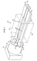
- the first preferred embodiment of an inventive Measuring tip 100 comprises a coplanar conductor structure 10 with a central one Signal conductor 12 and two coplanar arranged adjacent to this signal conductor 12 Ground conductor 14. Between the signal conductor 12 and a respective ground conductor 14, a predetermined gap 16 is formed.
- the coplanar conductor structure 10 extends from a coaxial cable side end 18 to a contact side End 20, and the gap 16 is over the entire length of the coplanar conductor pattern 10 formed such that a constant, predetermined characteristic impedance results.
- the coplanar conductor pattern 10 connected to a coaxial cable 22, wherein the signal conductor 12 a Inner conductor 24 and the ground conductor 14 an outer conductor 26 of the coaxial cable to contact.
- the quartz blocks 28 are with the coplanar conductor structure 10 firmly connected and each carry at their coplanar conductor structure 10 facing side of a metallization, which substantially the shape corresponds to the coplanar conductor structure 10 in the region of the quartz blocks 28.
- a metallization which substantially the shape corresponds to the coplanar conductor structure 10 in the region of the quartz blocks 28.
- the conductors 12, 14 are in a region 29 between the supporting quartz blocks 28 and the contact-side end 20 free arranged in space so that each conductor 12, 14 individually with respect to the holder can spring in the quartz blocks 28.
- this probe tip 100 mechanically to corresponding contact points for a testing electrical circuit pressed so requires the possibility of free Fedems for each individual conductor 12, 14 of the coplanar conductor structure 10 that each individual conductor 12, 14 an optimal contact with the respectively associated with him Contact point has.
- coplanar conductor structures with only two conductors 12, 14 are or more than three conductors 12, 14 possible, with the allocation of signal conductors and Ground conductors in the following way: g-s-g-s-g-s-g ... or g-s-g-g-s-g-g-s-g-g ... or similar. In this way are also to be tested electrical circuits Contactable with a single probe, which several coplanar signal lines exhibit.
- Fig. 2 second preferred embodiment of an inventive Measuring tip 200 substantially corresponds to that of Fig. 1, wherein like parts are identified by the same reference numerals, so that their Description is made to the above explanations with respect to Fig. 1.
- the quartz blocks 28 are at one of the coplanar Ladder structure 10 side facing away from a full-surface metallization 30 on. This metallization once leads to the suppression of unwanted modes higher order away from the desired operating frequency and creates at the same time over a predetermined area of the coplanar conductor structure 10 a closed System.
- FIG. 3 The illustrated in Fig. 3 third preferred embodiment of an inventive Measuring tip 300 illustrates the state after production of the measuring tip 300 with a method according to the invention on a silicon wafer.
- Fig. 3 are again the same parts with the same reference numerals, so for the explanation of the above description of FIGS. 1 and 2 referenced becomes.
- the conductors 12, 14 of the coplanar Ladder structure 10 initially after the production with a following even closer explained lithographic-electroforming method (LiGa method) via a bridge 32 mechanically connected to each other.
- a frame 34 is formed, which the coplanar conductor structure 10 in a Completely surrounding the plane.
- this frame 34 is a corresponding Handling the coplanar conductor structure 10 until the final completion of the Meßspitze possible, without the conductors 12, 14 even the coplanar conductor structure 10th to touch, with a corresponding risk of damage to this Conductors 12, 14.
- this arrangement 10, 32, 34 of the Silicon wafers are removed, and there are top and bottom in the corresponding Area of the widened gap 16, the quartz blocks 28, for example by means of Bonding attached to the coplanar conductor structure 10.
- the coplanar has Conductor structure 10 by the holder by means of the quartz blocks 28 an inherent stability, such that the connection between the coplanar conductor structure 10 and the bridge 32 with frame 34 can be separated. This is done, for example in the region of a schematically illustrated line 36. Expediently the separation takes place between the bridge 32 and the coplanar conductor structure 10 such that outer ends 38 of the two outer ground conductor 14 on coaxial cable side Survive the end of 18, so that an automatic centering of a coaxial cable to be connected to the coplanar conductor pattern 10.
- the conductors 12, 14 of the coplanar conductor structure are tapered 10 for forming an arrangement of the conductors 12, 14, which accordingly to be contacted contact points of an electrical circuit to be tested equivalent. Tapered to maintain a constant wave impedance in the region 29 at the contact end 20 of the gap 16 accordingly in the direction of the contact end 20.
- a particularly outstanding feature of the measuring tip according to the invention 1 to 3 is that the set by means of the column 16 impedance over the coplanar conductor structure 10 substantially free of dispersion is, i. the impedance and the phase velocity are essentially not dependent on the operating frequency.
- a silicon wafer 38 is vapor-deposited with a metal layer 40 (Fig. 4).
- the metal layer 40 includes, for example, titanium, silver, chromium or Gold.
- a photosensitive Paint 42 applied to the metal layer 40. This photosensitive varnish is exposed through a mask.
- the mask is designed such that they a certain number to be produced on the silicon wafer 38 coplanar Conductor structures 10 with respective bridge 32 and respective frame 34 corresponds, as shown in Fig. 3. Possibly. adjacent frames are mechanically interconnected connected.
- each individual coplanar conductor pattern 10 becomes within a frame 34 on both sides in the corresponding area with the quartz blocks 28 and finally the bridges 32 with frame 34 from the coplanar Conductor structures 10 separated.
- the coplanar conductor structure 10 connected to the coaxial cable end 18 with a coaxial cable.
- the individual conductors 12, 14 of the coplanar conductor structure 10 in any way in the Assembly must be aligned with each other.
- the relative arrangement of Ladder 12, 14 to each other is from the beginning to the end of the manufacturing process predetermined and fixed. This eliminates any tolerances in the mechanical Arranging the individual conductors 12, 14 in the manufacturing process
- the measuring tip according to the invention has a surprising effect good frequency behavior.
- Fig. 8 illustrates an S-parameter plot from a simulation calculation for a measuring tip according to the invention.
- a frequency in GHz on the horizontal axis 46 is a frequency in GHz and on the vertical axis 48 plotted an S-parameter in dB.
- the measuring tip according to the invention is according to this Model calculation up to frequencies of 60 GHz usable. This at the same time Possibility of mass production with low scrap and little effort.
Landscapes
- Physics & Mathematics (AREA)
- General Physics & Mathematics (AREA)
- Measuring Leads Or Probes (AREA)
- Testing Or Measuring Of Semiconductors Or The Like (AREA)
- Other Investigation Or Analysis Of Materials By Electrical Means (AREA)
- Investigating Or Analyzing Materials By The Use Of Electric Means (AREA)
- Measurement Of Resistance Or Impedance (AREA)
- Testing Of Individual Semiconductor Devices (AREA)
Description
- Fig. 1
- eine erste bevorzugte Ausführungsform einer erfindungsgemäßen Meßspitze in perspektivischer Ansicht,
- Fig. 2
- eine zweite bevorzugte Ausführungsform einer erfindungsgemäßen Meßspitze in perspektivischer Ansicht,
- Fig. 3
- eine dritte bevorzugte Ausführungsform einer erfindungsgemäßen Meßspitze in Aufsicht,
- Fig. 4 bis Fig. 7
- eine Veranschaulichung. aufeinanderfolgender Schritte eines erfindungsgemäßen Verfahrens und
- Fig. 8
- einen S-Parameter-Plott einer Simulationsrechnung für eine erfin-. dungsgemäße Meßspitze.
Claims (6)
- Meßspitze (100, 200, 300) zur Hochfrequenzmessung mit einem kontaktseitigen Ende (20) zum Kontaktieren von planaren Strukturen und einem koaxialkabelseitigen Ende (18) zum Verbinden mit einem Koaxialkabel (22), wobei zwischen dem kontaktseitigen Ende (20) und dem koaxialkabelseitigen Ende (18) eine koplanare Leiterstruktur (10) mit wenigstens zwei Leitern (12, 14) angeordnet ist, wobei auf der koplanaren Leiterstruktur (10) ein die koplanare Leiterstruktur (10) halterndes Dielektrikum (28) angeordnet ist,
dadurch gekennzeichnet, daß das Dielektrikum (28) auf der koplanaren Leiterstruktur (10) in einem mittleren Abschnitt zwischen und in Ausbreitungsrichtung beabstandet von dem koaxialkabelseitigen Ende (19) und dem kontaktseitigen Ende (20) wenigstens einseitig, insbesondere beidseitig, derart angeordnet ist, daß zwischen dem Dielektrikum (28) und dem kontaktseitigen Ende (20) jeder Leiter (12, 14) der koplanaren Leiterstruktur (10) individuell frei im Raum und bzgl. des halternden Dielektrikums (28) federnd ausgebildet ist, wobei zwischen je zwei Leitern (12, 14) der koplanaren Leiterstruktur (10) von dem koaxialkabelseitigen Ende (18) bis zum kontaktseitigen Ende (20) ein jeweiliger Spalt (16) derart ausgebildet ist, daß sich vom koaxialkabelseitigen Ende (18) bis zum kontaktseitigen Ende (20) ein konstanter Wellenwiderstand ergibt. - Meßspitze (100, 200, 300) nach Anspruch 1, dadurch gekennzeichnet, daß der jeweilige Spalt (16) im Bereich des Dielektrikums (28) breiter ausgebildet ist als in Bereich der koplanaren Leiterstruktur (10) ohne Dielektrikum (28).
- Meßspitze (100, 200, 300) nach einem der Ansprüche 1 oder 2, dadurch gekennzeichnet, daß das Dielektrikum als wenigstens ein Quarzblock (28) ausgebildet ist.
- Meßspitze (100, 200, 300) nach wenigstens einem der vorhergehenden Ansprüche, dadurch gekennzeichnet, daß das Dielektrikum (28) an einer Verbindungsseite mit der koplanaren Leiterstruktur (10) eine sich mit letzterer im wesentlichen deckende Metallbeschichtung aufweist.
- Meßspitze (200) nach wenigstens einem der vorhergehenden Ansprüche, dadurch gekennzeichnet, daß das Dielektrikum (28) an einer der koplanaren Leiterstruktur abgewandten Seite vollflächig metallisiert ist.
- Meßspitze nach wenigstens einem der vorhergehenden Ansprüche, dadurch gekennzeichnet, daß am koaxialkabelseitigen Ende (18) eine planare Schaltung, insbesondere eine elektrische, elektronische bzw. aktive Schaltung, oder wenigstens ein aktives Schaltungselement, angeordnet ist.
Applications Claiming Priority (3)
| Application Number | Priority Date | Filing Date | Title |
|---|---|---|---|
| DE19945178 | 1999-09-21 | ||
| DE19945178A DE19945178C2 (de) | 1999-09-21 | 1999-09-21 | Meßspitze zur Hochfrequenzmessung und Verfahren zu deren Herstellung |
| PCT/DE2000/003231 WO2001022097A1 (de) | 1999-09-21 | 2000-09-18 | Messspitze zur hochfrequenzmessung und verfahren zu deren herstellung |
Publications (2)
| Publication Number | Publication Date |
|---|---|
| EP1216419A1 EP1216419A1 (de) | 2002-06-26 |
| EP1216419B1 true EP1216419B1 (de) | 2004-03-10 |
Family
ID=7922746
Family Applications (1)
| Application Number | Title | Priority Date | Filing Date |
|---|---|---|---|
| EP00978936A Expired - Lifetime EP1216419B1 (de) | 1999-09-21 | 2000-09-18 | Me spitze zur Hochfrequenzmessung |
Country Status (11)
| Country | Link |
|---|---|
| US (1) | US7042236B1 (de) |
| EP (1) | EP1216419B1 (de) |
| JP (1) | JP2003510574A (de) |
| CN (1) | CN1162707C (de) |
| AT (1) | ATE261585T1 (de) |
| CA (1) | CA2385337C (de) |
| DE (2) | DE19945178C2 (de) |
| DK (1) | DK1216419T3 (de) |
| ES (1) | ES2214335T3 (de) |
| PT (1) | PT1216419E (de) |
| WO (1) | WO2001022097A1 (de) |
Families Citing this family (28)
| Publication number | Priority date | Publication date | Assignee | Title |
|---|---|---|---|---|
| CA2336531A1 (en) * | 1998-07-08 | 2000-01-20 | Capres Aps | Multi-point probe |
| JP4678993B2 (ja) * | 2001-06-19 | 2011-04-27 | 日置電機株式会社 | 高周波プローブおよび高周波プローブの製造方法 |
| DE10136726A1 (de) * | 2001-07-27 | 2003-04-03 | Connexion Rosenberger Gmbh | Meßanordnung für Hochfrequenzmessungen mit mehreren Meßsonden und ein Verfahren zur Herstellung derselben |
| DE10201491C1 (de) * | 2002-01-16 | 2003-08-28 | Gfd Ges Fuer Diamantprodukte M | Meßspitzensystem und Verfahren zu dessen Herstellung |
| DE10229038B4 (de) * | 2002-06-28 | 2013-08-14 | Robert Bosch Gmbh | Verkapptes Mikrostrukturbauelement mit Hochfrequenzdurchführung |
| DE202004021093U1 (de) * | 2003-12-24 | 2006-09-28 | Cascade Microtech, Inc., Beaverton | Aktiver Halbleiterscheibenmessfühler |
| US7344381B2 (en) * | 2004-04-29 | 2008-03-18 | Emerson Network Power Connectivity Solutions, Inc. | High frequency edge mount connector |
| US7056134B2 (en) * | 2004-05-27 | 2006-06-06 | Tektronix, Inc. | Attachable/detachable probing tip system for a measurement probing system |
| DE202004019636U1 (de) * | 2004-12-20 | 2005-03-03 | Rosenberger Hochfrequenztechnik Gmbh & Co. Kg | Meßspitze für HF-Messung |
| RU2285930C1 (ru) * | 2005-04-11 | 2006-10-20 | Федеральное государственное унитарное предприятие "Научно-производственное предприятие "Исток" (ФГУП НПП "Исток") | Зонд для измерения электрических характеристик планарных элементов интегральных схем |
| JP4679244B2 (ja) * | 2005-05-26 | 2011-04-27 | 株式会社アドバンテスト | 測定用コンタクト端子、測定装置、プローブカードセット、およびウエハプローバ装置 |
| DE202006006359U1 (de) * | 2006-04-20 | 2006-07-13 | Rosenberger Hochfrequenztechnik Gmbh & Co. Kg | Potentialfreie Gehäusedurchführung |
| DE102007006195A1 (de) * | 2007-02-07 | 2008-08-14 | Infineon Technologies Ag | Kontaktelement, Kontakteinheit, Verfahren zur Herstellung einer Kontakteinheit und Verfahren zur Inbetriebnahme für Fine-Pitch Bauteile |
| US7982480B2 (en) * | 2008-08-01 | 2011-07-19 | Aes Technologies, Inc. | Calibrated wideband high frequency passive impedance probe |
| DE202008010533U1 (de) * | 2008-08-07 | 2008-10-30 | Rosenberger Hochfrequenztechnik Gmbh & Co. Kg | Kontaktlose Schleifensonde |
| DE202008013982U1 (de) * | 2008-10-20 | 2009-01-08 | Rosenberger Hochfrequenztechnik Gmbh & Co. Kg | Messsystem zum Bestimmen von Streuparametern |
| DE202009003966U1 (de) * | 2009-03-20 | 2009-06-04 | Rosenberger Hochfrequenztechnik Gmbh & Co. Kg | Messspitzen |
| DE202012002391U1 (de) | 2012-03-08 | 2013-06-10 | Rosenberger Hochfrequenztechnik Gmbh & Co. Kg | Vorrichtung zur Messung elektronischer Bauteile |
| DE102012107556A1 (de) * | 2012-08-17 | 2014-02-20 | HARTING Electronics GmbH | Vorrichtung und Verfahren zur reversiblen, mechanischen Fixierung und elektrischen Kontaktierung elektrischer Leiter |
| DE202014002841U1 (de) | 2014-04-01 | 2014-06-25 | Rosenberger Hochfrequenztechnik Gmbh & Co. Kg | Kontaktieranordnung, insbesondere HF-Messspitze |
| CN105092975B (zh) * | 2015-09-23 | 2017-11-03 | 广州兴森快捷电路科技有限公司 | Pcb板内单端阻抗测试头 |
| US11041880B2 (en) * | 2017-12-01 | 2021-06-22 | Tektronix, Inc. | Contactless coupling between test and measurement system and a device under test |
| DE102018104264A1 (de) * | 2018-02-26 | 2019-08-29 | Rosenberger Hochfrequenztechnik Gmbh & Co. Kg | Verfahren zur herstellung von mindestens einem hochfrequenz-kontaktelement oder einer hochfrequenz-kontaktelement-anordnung sowie zugehörige vorrichtung |
| WO2020022085A1 (ja) * | 2018-07-27 | 2020-01-30 | 日置電機株式会社 | 測定装置 |
| JP7387285B2 (ja) | 2019-04-26 | 2023-11-28 | 日置電機株式会社 | プローブ装置 |
| TWI889840B (zh) * | 2020-06-11 | 2025-07-11 | 美商鋒法特股份有限公司 | 多導體傳輸線探針及其探針頭 |
| CN112993058B (zh) * | 2021-02-03 | 2023-11-24 | 中国电子科技集团公司第四十三研究所 | 一种基于混合集成工艺的光电微系统封装结构 |
| JP7676231B2 (ja) * | 2021-06-02 | 2025-05-14 | 株式会社日本マイクロニクス | プローブユニット |
Family Cites Families (18)
| Publication number | Priority date | Publication date | Assignee | Title |
|---|---|---|---|---|
| US4697143A (en) * | 1984-04-30 | 1987-09-29 | Cascade Microtech, Inc. | Wafer probe |
| JPH0669054B2 (ja) * | 1986-04-09 | 1994-08-31 | 田中貴金属工業株式会社 | 半導体ウエ−ハの電気的特性測定用プロ−ブ針 |
| US4894612A (en) | 1987-08-13 | 1990-01-16 | Hypres, Incorporated | Soft probe for providing high speed on-wafer connections to a circuit |
| US4871964A (en) * | 1988-04-12 | 1989-10-03 | G. G. B. Industries, Inc. | Integrated circuit probing apparatus |
| JP2704305B2 (ja) * | 1990-03-15 | 1998-01-26 | 日本エー・エム・ピー株式会社 | 高周波コネクタ及びその製造方法 |
| JPH0427874A (ja) * | 1990-05-22 | 1992-01-30 | Mitsubishi Electric Corp | 高周波素子測定用プローブヘッド |
| US5512838A (en) * | 1992-09-03 | 1996-04-30 | Hewlett-Packard Company | Probe with reduced input capacitance |
| US5373231A (en) * | 1993-06-10 | 1994-12-13 | G. G. B. Industries, Inc. | Integrated circuit probing apparatus including a capacitor bypass structure |
| US5561378A (en) * | 1994-07-05 | 1996-10-01 | Motorola, Inc. | Circuit probe for measuring a differential circuit |
| US5506515A (en) * | 1994-07-20 | 1996-04-09 | Cascade Microtech, Inc. | High-frequency probe tip assembly |
| US5565788A (en) * | 1994-07-20 | 1996-10-15 | Cascade Microtech, Inc. | Coaxial wafer probe with tip shielding |
| US5508630A (en) * | 1994-09-09 | 1996-04-16 | Board Of Regents, University Of Texas Systems | Probe having a power detector for use with microwave or millimeter wave device |
| DE19641880A1 (de) * | 1996-10-10 | 1998-04-16 | Rosenberger Hochfrequenztech | Meßspitzeneinheit zum Kontaktieren von planaren Mikrowellenschaltungen |
| JPH10327004A (ja) * | 1997-05-22 | 1998-12-08 | Hitachi Ltd | 同軸コネクタを有する回路モジュール |
| JPH1174396A (ja) * | 1997-08-28 | 1999-03-16 | Kyocera Corp | 高周波用入出力端子ならびに高周波用半導体素子収納用パッケージ |
| JP3100930B2 (ja) * | 1997-09-10 | 2000-10-23 | 株式会社双晶テック | コンタクトプローブ |
| JP3439967B2 (ja) * | 1997-11-28 | 2003-08-25 | 京セラ株式会社 | 高周波半導体素子用パッケージ |
| US6118287A (en) * | 1997-12-09 | 2000-09-12 | Boll; Gregory George | Probe tip structure |
-
1999
- 1999-09-21 DE DE19945178A patent/DE19945178C2/de not_active Expired - Fee Related
-
2000
- 2000-09-18 DK DK00978936T patent/DK1216419T3/da active
- 2000-09-18 US US10/088,591 patent/US7042236B1/en not_active Expired - Lifetime
- 2000-09-18 AT AT00978936T patent/ATE261585T1/de active
- 2000-09-18 CN CNB008128677A patent/CN1162707C/zh not_active Expired - Lifetime
- 2000-09-18 PT PT00978936T patent/PT1216419E/pt unknown
- 2000-09-18 ES ES00978936T patent/ES2214335T3/es not_active Expired - Lifetime
- 2000-09-18 WO PCT/DE2000/003231 patent/WO2001022097A1/de not_active Ceased
- 2000-09-18 JP JP2001525416A patent/JP2003510574A/ja active Pending
- 2000-09-18 DE DE50005616T patent/DE50005616D1/de not_active Expired - Lifetime
- 2000-09-18 CA CA002385337A patent/CA2385337C/en not_active Expired - Fee Related
- 2000-09-18 EP EP00978936A patent/EP1216419B1/de not_active Expired - Lifetime
Also Published As
| Publication number | Publication date |
|---|---|
| EP1216419A1 (de) | 2002-06-26 |
| CN1162707C (zh) | 2004-08-18 |
| DE50005616D1 (de) | 2004-04-15 |
| ES2214335T3 (es) | 2004-09-16 |
| WO2001022097A1 (de) | 2001-03-29 |
| PT1216419E (pt) | 2004-07-30 |
| ATE261585T1 (de) | 2004-03-15 |
| DK1216419T3 (da) | 2004-07-12 |
| DE19945178C2 (de) | 2003-05-28 |
| US7042236B1 (en) | 2006-05-09 |
| DE19945178A1 (de) | 2001-08-02 |
| JP2003510574A (ja) | 2003-03-18 |
| CA2385337C (en) | 2010-01-12 |
| CN1373853A (zh) | 2002-10-09 |
| CA2385337A1 (en) | 2001-03-29 |
Similar Documents
| Publication | Publication Date | Title |
|---|---|---|
| DE19945178C2 (de) | Meßspitze zur Hochfrequenzmessung und Verfahren zu deren Herstellung | |
| DE69620673T2 (de) | Senkrechte Mikrowellenverbindung mittels Anordnung mit kompressiblem Leiter | |
| DE4310288B4 (de) | Oberflächenmontierbarer Widerstand | |
| DE3639367C2 (de) | ||
| DE2800745A1 (de) | Elektrischer verbinder | |
| DE102009019626B3 (de) | Elektrischer Verbinder mit Impedanzkorrekturelement und Verfahren zu seiner Herstellung | |
| DE202004021017U1 (de) | Messsonden-Prüfstruktur | |
| DE69012732T2 (de) | Durchgehende Verbindungen in Mehrschichtschaltungen. | |
| DE10143173A1 (de) | Wafersonde | |
| DE69216742T2 (de) | Breitbandiger Übergang zwischen einer Mikrostreifenleitung und einer Schlitzleitung | |
| EP2409166B1 (de) | Hochfrequenz-Messpitze | |
| DE1949966B2 (de) | Nockeschalter für Hochfrequenz | |
| EP3555967B1 (de) | Verfahren zur herstellung von mindestens einem hochfrequenz-kontaktelement oder einer hochfrequenz-kontaktelement-anordnung sowie zugehörige vorrichtungen | |
| DE69217848T2 (de) | Koaxialleiter/Mikrostreifenleitungsübergang | |
| DE69424544T2 (de) | Isolations-mittel zur störstrahlungsunterdrückung in einem elektrischen feld | |
| DE69925873T2 (de) | Hochfrequenzschalter | |
| DE69714444T2 (de) | Keramikfilter mit koplanarer abschirmung | |
| DE112017007145T5 (de) | Zwischenplattenverbindungsstruktur | |
| DE102007046351B4 (de) | Hochfrequenzplatine, die einen Übertragungsmodus von Hochfrequenzsignalen wandelt | |
| DE69206325T2 (de) | Mikrowellenverbinderanordnung mit einfachem Anschluss an Mikrowellenschaltelemente. | |
| WO2010003665A1 (de) | Streifenleitung mit durchkontaktierung | |
| EP1174922B1 (de) | Gehäuse für eine integrierte Schaltung mit Koplanarleitungen | |
| DE10132127C1 (de) | Bewegbarer Kontaktträger für einen Niederspannungs-Leistungsschalter und Verfahren zu seiner Herstellung | |
| DE69811069T2 (de) | Verfahren und vorrichtung zum verbinden zweier millimeterelemente | |
| EP2137787B1 (de) | Gleichspannungstrenner |
Legal Events
| Date | Code | Title | Description |
|---|---|---|---|
| PUAI | Public reference made under article 153(3) epc to a published international application that has entered the european phase |
Free format text: ORIGINAL CODE: 0009012 |
|
| 17P | Request for examination filed |
Effective date: 20020417 |
|
| AK | Designated contracting states |
Kind code of ref document: A1 Designated state(s): AT BE CH CY DE DK ES FI FR GB GR IE IT LI LU MC NL PT SE |
|
| REG | Reference to a national code |
Ref country code: GB Ref legal event code: FG4D Free format text: NOT ENGLISH |
|
| GRAP | Despatch of communication of intention to grant a patent |
Free format text: ORIGINAL CODE: EPIDOSNIGR1 |
|
| RTI1 | Title (correction) |
Free format text: MEASURING PROBE FOR MEASURING HIGH FREQUENCIES |
|
| GRAS | Grant fee paid |
Free format text: ORIGINAL CODE: EPIDOSNIGR3 |
|
| GRAA | (expected) grant |
Free format text: ORIGINAL CODE: 0009210 |
|
| AK | Designated contracting states |
Kind code of ref document: B1 Designated state(s): AT BE CH CY DE DK ES FI FR GB GR IE IT LI LU MC NL PT SE |
|
| PG25 | Lapsed in a contracting state [announced via postgrant information from national office to epo] |
Ref country code: CY Free format text: LAPSE BECAUSE OF FAILURE TO SUBMIT A TRANSLATION OF THE DESCRIPTION OR TO PAY THE FEE WITHIN THE PRESCRIBED TIME-LIMIT Effective date: 20040310 |
|
| REG | Reference to a national code |
Ref country code: CH Ref legal event code: EP |
|
| REG | Reference to a national code |
Ref country code: IE Ref legal event code: FG4D Free format text: GERMAN |
|
| REF | Corresponds to: |
Ref document number: 50005616 Country of ref document: DE Date of ref document: 20040415 Kind code of ref document: P |
|
| REG | Reference to a national code |
Ref country code: CH Ref legal event code: NV Representative=s name: HANS RUDOLF GACHNANG PATENTANWALT |
|
| REG | Reference to a national code |
Ref country code: SE Ref legal event code: TRGR |
|
| GBT | Gb: translation of ep patent filed (gb section 77(6)(a)/1977) |
Effective date: 20040608 |
|
| REG | Reference to a national code |
Ref country code: DK Ref legal event code: T3 |
|
| REG | Reference to a national code |
Ref country code: GR Ref legal event code: EP Ref document number: 20040401830 Country of ref document: GR |
|
| REG | Reference to a national code |
Ref country code: PT Ref legal event code: SC4A Free format text: AVAILABILITY OF NATIONAL TRANSLATION Effective date: 20040527 |
|
| REG | Reference to a national code |
Ref country code: ES Ref legal event code: FG2A Ref document number: 2214335 Country of ref document: ES Kind code of ref document: T3 |
|
| PG25 | Lapsed in a contracting state [announced via postgrant information from national office to epo] |
Ref country code: LU Free format text: LAPSE BECAUSE OF NON-PAYMENT OF DUE FEES Effective date: 20040918 |
|
| PG25 | Lapsed in a contracting state [announced via postgrant information from national office to epo] |
Ref country code: MC Free format text: LAPSE BECAUSE OF NON-PAYMENT OF DUE FEES Effective date: 20040930 |
|
| ET | Fr: translation filed | ||
| PLBE | No opposition filed within time limit |
Free format text: ORIGINAL CODE: 0009261 |
|
| STAA | Information on the status of an ep patent application or granted ep patent |
Free format text: STATUS: NO OPPOSITION FILED WITHIN TIME LIMIT |
|
| 26N | No opposition filed |
Effective date: 20041213 |
|
| REG | Reference to a national code |
Ref country code: CH Ref legal event code: NV Representative=s name: GACHNANG AG PATENTANWAELTE, CH |
|
| REG | Reference to a national code |
Ref country code: FR Ref legal event code: PLFP Year of fee payment: 17 |
|
| REG | Reference to a national code |
Ref country code: FR Ref legal event code: PLFP Year of fee payment: 18 |
|
| REG | Reference to a national code |
Ref country code: FR Ref legal event code: PLFP Year of fee payment: 19 |
|
| PGFP | Annual fee paid to national office [announced via postgrant information from national office to epo] |
Ref country code: IE Payment date: 20180925 Year of fee payment: 19 |
|
| PGFP | Annual fee paid to national office [announced via postgrant information from national office to epo] |
Ref country code: SE Payment date: 20180926 Year of fee payment: 19 Ref country code: GR Payment date: 20180925 Year of fee payment: 19 |
|
| PGFP | Annual fee paid to national office [announced via postgrant information from national office to epo] |
Ref country code: PT Payment date: 20180828 Year of fee payment: 19 |
|
| PGFP | Annual fee paid to national office [announced via postgrant information from national office to epo] |
Ref country code: ES Payment date: 20181024 Year of fee payment: 19 |
|
| PGFP | Annual fee paid to national office [announced via postgrant information from national office to epo] |
Ref country code: FR Payment date: 20190925 Year of fee payment: 20 Ref country code: NL Payment date: 20190926 Year of fee payment: 20 Ref country code: IT Payment date: 20190923 Year of fee payment: 20 |
|
| PGFP | Annual fee paid to national office [announced via postgrant information from national office to epo] |
Ref country code: BE Payment date: 20190926 Year of fee payment: 20 |
|
| PGFP | Annual fee paid to national office [announced via postgrant information from national office to epo] |
Ref country code: GB Payment date: 20190930 Year of fee payment: 20 Ref country code: AT Payment date: 20190920 Year of fee payment: 20 |
|
| PGFP | Annual fee paid to national office [announced via postgrant information from national office to epo] |
Ref country code: DE Payment date: 20191129 Year of fee payment: 20 Ref country code: CH Payment date: 20190925 Year of fee payment: 20 |
|
| REG | Reference to a national code |
Ref country code: FI Ref legal event code: MAE |
|
| REG | Reference to a national code |
Ref country code: DK Ref legal event code: EBP Effective date: 20190930 |
|
| PG25 | Lapsed in a contracting state [announced via postgrant information from national office to epo] |
Ref country code: FI Free format text: LAPSE BECAUSE OF NON-PAYMENT OF DUE FEES Effective date: 20190918 Ref country code: SE Free format text: LAPSE BECAUSE OF NON-PAYMENT OF DUE FEES Effective date: 20190919 |
|
| REG | Reference to a national code |
Ref country code: SE Ref legal event code: EUG |
|
| PG25 | Lapsed in a contracting state [announced via postgrant information from national office to epo] |
Ref country code: IE Free format text: LAPSE BECAUSE OF NON-PAYMENT OF DUE FEES Effective date: 20190918 Ref country code: PT Free format text: LAPSE BECAUSE OF NON-PAYMENT OF DUE FEES Effective date: 20200421 Ref country code: GR Free format text: LAPSE BECAUSE OF NON-PAYMENT OF DUE FEES Effective date: 20200416 |
|
| REG | Reference to a national code |
Ref country code: DE Ref legal event code: R071 Ref document number: 50005616 Country of ref document: DE |
|
| REG | Reference to a national code |
Ref country code: NL Ref legal event code: MK Effective date: 20200917 |
|
| REG | Reference to a national code |
Ref country code: CH Ref legal event code: PL |
|
| REG | Reference to a national code |
Ref country code: GB Ref legal event code: PE20 Expiry date: 20200917 |
|
| REG | Reference to a national code |
Ref country code: BE Ref legal event code: MK Effective date: 20200918 |
|
| PG25 | Lapsed in a contracting state [announced via postgrant information from national office to epo] |
Ref country code: DK Free format text: LAPSE BECAUSE OF NON-PAYMENT OF DUE FEES Effective date: 20190930 Ref country code: PT Free format text: LAPSE BECAUSE OF EXPIRATION OF PROTECTION Effective date: 20200928 Ref country code: GB Free format text: LAPSE BECAUSE OF EXPIRATION OF PROTECTION Effective date: 20200917 |
|
| REG | Reference to a national code |
Ref country code: AT Ref legal event code: MK07 Ref document number: 261585 Country of ref document: AT Kind code of ref document: T Effective date: 20200918 |
|
| REG | Reference to a national code |
Ref country code: ES Ref legal event code: FD2A Effective date: 20210128 |
|
| PG25 | Lapsed in a contracting state [announced via postgrant information from national office to epo] |
Ref country code: ES Free format text: LAPSE BECAUSE OF NON-PAYMENT OF DUE FEES Effective date: 20190919 |
|
| PG25 | Lapsed in a contracting state [announced via postgrant information from national office to epo] |
Ref country code: PT Free format text: LAPSE BECAUSE OF NON-PAYMENT OF DUE FEES Effective date: 20190918 |
|
| PG25 | Lapsed in a contracting state [announced via postgrant information from national office to epo] |
Ref country code: PT Free format text: LAPSE BECAUSE OF NON-PAYMENT OF DUE FEES Effective date: 20190918 |