EP1202130B1 - Image forming apparatus - Google Patents
Image forming apparatus Download PDFInfo
- Publication number
- EP1202130B1 EP1202130B1 EP01125796A EP01125796A EP1202130B1 EP 1202130 B1 EP1202130 B1 EP 1202130B1 EP 01125796 A EP01125796 A EP 01125796A EP 01125796 A EP01125796 A EP 01125796A EP 1202130 B1 EP1202130 B1 EP 1202130B1
- Authority
- EP
- European Patent Office
- Prior art keywords
- voltage
- recording material
- transferring member
- image
- transfer
- Prior art date
- Legal status (The legal status is an assumption and is not a legal conclusion. Google has not performed a legal analysis and makes no representation as to the accuracy of the status listed.)
- Expired - Lifetime
Links
- 239000000463 material Substances 0.000 claims description 90
- 230000015572 biosynthetic process Effects 0.000 claims description 4
- 230000000630 rising effect Effects 0.000 description 6
- 230000000694 effects Effects 0.000 description 4
- 239000011800 void material Substances 0.000 description 4
- 230000000052 comparative effect Effects 0.000 description 3
- 238000000034 method Methods 0.000 description 3
- 238000011144 upstream manufacturing Methods 0.000 description 3
- 230000007547 defect Effects 0.000 description 2
- 230000008569 process Effects 0.000 description 2
- 230000004044 response Effects 0.000 description 2
- XAGFODPZIPBFFR-UHFFFAOYSA-N aluminium Chemical compound [Al] XAGFODPZIPBFFR-UHFFFAOYSA-N 0.000 description 1
- 229910052782 aluminium Inorganic materials 0.000 description 1
- 238000004140 cleaning Methods 0.000 description 1
- 230000001419 dependent effect Effects 0.000 description 1
- 238000001514 detection method Methods 0.000 description 1
- 238000011161 development Methods 0.000 description 1
- 230000018109 developmental process Effects 0.000 description 1
- 230000006870 function Effects 0.000 description 1
- 238000012986 modification Methods 0.000 description 1
- 230000004048 modification Effects 0.000 description 1
- 230000002093 peripheral effect Effects 0.000 description 1
- 230000009467 reduction Effects 0.000 description 1
- 239000004065 semiconductor Substances 0.000 description 1
Images


Classifications
-
- G—PHYSICS
- G03—PHOTOGRAPHY; CINEMATOGRAPHY; ANALOGOUS TECHNIQUES USING WAVES OTHER THAN OPTICAL WAVES; ELECTROGRAPHY; HOLOGRAPHY
- G03G—ELECTROGRAPHY; ELECTROPHOTOGRAPHY; MAGNETOGRAPHY
- G03G15/00—Apparatus for electrographic processes using a charge pattern
- G03G15/14—Apparatus for electrographic processes using a charge pattern for transferring a pattern to a second base
- G03G15/16—Apparatus for electrographic processes using a charge pattern for transferring a pattern to a second base of a toner pattern, e.g. a powder pattern, e.g. magnetic transfer
- G03G15/1665—Apparatus for electrographic processes using a charge pattern for transferring a pattern to a second base of a toner pattern, e.g. a powder pattern, e.g. magnetic transfer by introducing the second base in the nip formed by the recording member and at least one transfer member, e.g. in combination with bias or heat
- G03G15/167—Apparatus for electrographic processes using a charge pattern for transferring a pattern to a second base of a toner pattern, e.g. a powder pattern, e.g. magnetic transfer by introducing the second base in the nip formed by the recording member and at least one transfer member, e.g. in combination with bias or heat at least one of the recording member or the transfer member being rotatable during the transfer
- G03G15/1675—Apparatus for electrographic processes using a charge pattern for transferring a pattern to a second base of a toner pattern, e.g. a powder pattern, e.g. magnetic transfer by introducing the second base in the nip formed by the recording member and at least one transfer member, e.g. in combination with bias or heat at least one of the recording member or the transfer member being rotatable during the transfer with means for controlling the bias applied in the transfer nip
Definitions
- the present invention relates to an image forming apparatus such as a printer, copying machine, facsimile machine or the like.
- FIG. 7 there is shown a structure of a transfer portion of an image forming apparatus such as a printer according to a background art.
- the photosensitive drum 1 is rotated in the direction indicated by an arrow R1, and a toner image is formed thereon by charging means, exposure means and developing means (unshown).
- the toner image is transferred onto a recording material such as paper by a transfer roller (transferring means).
- the transfer roller 2 is contacted to the photosensitive drum 1 to form a transfer nip T therebetween.
- the transfer roller 2 is supplied with a high voltage (transfer bias) from a high voltage source (transfer bias application voltage source).
- the voltage applied to the transfer roller 2 is controlled through a predetermined sequence by control means 4, and the current flowing through the transfer roller 2 is detected by current detecting means 5.
- the distance from the sensor 7 to the transfer nip T is set to L.
- Figure 8 shows a voltage applied to the transfer roller 2 when the printing (image formation) is carried out on one recording material.
- the abscissa represents time, and ordinate represents presence or absence of the recording material and the voltage (transfer bias).
- the time 0 corresponds to the time when the user instructs the printing operation.
- the control means 4 adjusts the voltage such that current detected by the current detecting means 5 is a predetermined value.
- the current is 2 ⁇ A, for example. Since the resistance value of the transfer roller 2 varies depending on the ambient conditions under which the apparatus is used and on the transfer rollers, the voltage is adjusted to provide a proper current for image transfer operation.
- the voltage required for flowing the current suitable for the image transfer is designated by C in Figure 8 .
- the high voltage source 3 is controlled at time A which is t1 after C, such that voltage D is applied from the point of time (time a) when the sensor 7 detects the presence of the sheet after the recording material is fed to the point of time at which the recording material reaches the transfer nip T.
- time b At the time when the sensor 7 detects the absence of the recording material (time b) is deemed as being the point of time at which the trailing-edge of the recording material passes, and the high voltage source 3 is controlled at time B t2 thereafter, such that voltage restores to C prior to the trading edge of the recording material passes the transfer nip T.
- the output of the voltage is stopped at proper timing.
- the voltage is raised during the recording material being in the transfer nip T, in order to compensate the reduction of the current which otherwise occurs because of the existence of the recording material in the transfer nip T.
- the voltage D is not applied from the initial stage, because the high voltage across the transfer nip T without the recording material in the need may damage the photosensitive drum 1.
- the setting is selected so as to assure that voltage D is reached only after the recording material come into the transfer nip T, even when the rising time Fair t is minimum.
- the toner is not sufficiently transferred from the photosensitive drum to the recording material after the leading-edge of the recording material to the arrival of the voltage from the high voltage source 3 at voltage D (image defect of transfer void). If, on the other hand, the voltage D is too high, the toner jumps so vigorously at the recording material that image defect occurs due to the so-called scattering of the toner.
- an apparatus according to the preamble of claim 1 is disclosed in particular, there is disclosed an image forming apparatus, wherein the voltage applying means applies a voltage to the charging member so that the charging member is constant-voltage controlled when an image region of the image bearing member is in the transfer station, and the charging member is constant-current-controlled during at least a part of a period when it is not in the transfer station.
- a voltage applied during the constant voltage control is a voltage appearing in the transfer device during the constant current control multiplied by a coefficient being larger than 1.
- a second voltage is applied, then a third voltage is applied, and then the second voltage is applied again. Thereby, the boundary regions of the recording material are treated different from the middle region thereof.
- an image forming apparatus as set out in claim 1.
- Figure 1 illustrates an example of an image forming apparatus according to a comparative example being not covered by the present invention.
- This Figure is a longitudinal sectional view of the apparatus which is a printer.
- the printer includes an electrophotographic photosensitive member (image bearing member) in the form of a drum (photosensitive drum) 11.
- the photosensitive drum 11 make comprises an electroconductive drum base member of aluminum or the like, and an OPC (organic light semiconductor) provided on the outer surface of the drum base member as a photosensitive layer.
- the photosensitive drum 11 is driven in the direction indicated by an arrow R11 by a driving means (unshown) at a predetermined process speed (peripheral speed).
- charger (charging means) 12 having a charging roller (charge member), an exposure device (exposure means) 13, a developing device (developing means) 14, a transfer device (transferring means) 15 having a transfer roller (transferring member), and a cleaner (cleaning means) 21, in the order named along the periphery of the photosensitive drum 11.
- the transfer roller 15 is connected with a high voltage source (transfer bias application voltage source) 16 which is in turn connected with a control means 17. Between the transfer roller 15 and the high voltage source 16, there is a current detecting means 18 connected with the control means 17.
- the transfer roller 15 is contacted to the bottom portion of the surface of the photosensitive drum 11 to form a transfer nip (transfer portion) T between itself and the photosensitive drum 11.
- the feeding path 19 for the recording material extends from the left side to the righthand side, and a recording material sensor (recording material detecting means) 20 for detecting the recording material is disposed upstream of the transfer nip T with respect to the recording material feeding direction (arrow Kp).
- the distance between the transfer nip T and the recording material sensor 20 is set at L.
- Designated by 22 is a sheet feeding tray; 23 is a sheet feeding roller (sheet feeding means); 24 is a registration roller (registration means).
- the recording material is picked up by the sheet feeding roller 23 from the sheet feeding tray 22, and is fed to the registration roller 24 where the recording material is temporarily stopped for synchronization with the image on the photosensitive drum 11. Thereafter, the recording material is fed into the transfer nip T by the registration roller 24 which is started in response to a synchronizing signal thereafter.
- the description will be made as to operations of the image forming apparatus having the above-described structure.
- the photosensitive drum 11 When the user instructs the printing operation (image formation), that is, a print starting signal is produced, the photosensitive drum 11 is rotated in the direction indicated by an arrow R11 by driving means (unshown). The surface of the photosensitive drum 11 is uniformly charged to a predetermined potential of a predetermined polarity by the charging roller 12. The surface of the photosensitive drum 11 after the electrical charging, is exposed to image light by the exposure device 13 so that and electrostatic latent image is formed. Electrostatic latent image is developed with toner by the developing device 14 into a toner image.
- the toner image thus formed on the surface of the photosensitive drum 11 is transfer onto a recording material P supplied into the transfer nip T along the feeding path 19 in the direction indicated by the arrow Kp, by application of the transfer bias voltage to the transfer roller 15.
- the photosensitive drum 11 after the toner image transfer is clean by a cleaner 21 such that toner remaining on the surface thereof is removed, so that photosensitive drum 11 is prepared for the next image formation.
- the recording material P after the toner image transfer is subjected to heat and pressure by the fixing device 25 so that toner image is fixed on the surface of the recording material P.
- the recording material P is discharged to an outside of the main assembly of the image forming apparatus, was finishing the printing (image forming) operation.
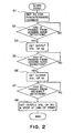
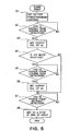
- Figure 1 is a schematic illustration of the image forming apparatus, as stated hereinbefore, Figure 2 is a flow chart of operation, and Figure 3 is a timing chart.
- the control means 17 activate the high voltage source 16 and effects control such that current through the current detecting means 18 is at a predetermined level.
- the voltage (first voltage) at which the current flowing through the current detecting means 18 is the predetermined level (VO at S1 in Figure 2 ) is stored in voltage storing means 17a.
- the resistance value of the transfer roller 15 varies depending on the individual rollers, the ambient condition difference such as a temperature and a humidity. The range of variation is approximately from 400M ⁇ to 2000M ⁇ . Therefore, at the start of printed operation, the voltage is preferably adjusted by the above-described step S1.
- the voltage VO is maintained until the recording material sensor 20 detects the recording material P.
- the timing at which the recording material sensor 20 detects the sheet that is, the timing at which the output signal is produced by the recording material sensor (a reference signal for the transfer voltage control), is indicated by time an in Figure 3 .
- the control means 17 controls the high voltage source 16 such that high voltage source 16 produces a voltage Vp (second voltage) which is higher than the voltage VO (S3).
- Vp second voltage
- t3 is set to be the time prior to the recording material P is nipped by the transfer nip T, more particularly, it is set to satisfy t3 ⁇ L/S where L is a distance between the recording material sensor 20 and the transfer nip T, and S is a feeding speed of the recording material.
- the control means 17 sets the high voltage source 16 so as to produce a voltage Vh (voltage Vh) which is higher than Vp (S6).
- the t4 is selected such that recording material P is nipped in the transfer nip T, that is, t4 satisfies t4 ⁇ L/S.
- the control means 17 sets the high voltage source 16 so as to produce the voltage VO (S8), and the high voltage source 16 is deactivated upon the finishing of the printing operation.
- Fair t1 in Figure 3 is a rising time period required for raising the voltage from V0 to Vp
- Fair t2 is a rising time period required for raising the voltage from Vp to Vh.
- the voltage produced by the high voltage source 16 when the voltage produced by the high voltage source 16 is raised to a high level, the voltage is first raised to a predetermined voltage Vp prior to the recording material reaching the transfer nip T, and the voltage is then raised to the final target voltage Vh when the recording material is assuredly present in the transfer nip T.
- the voltage is stepwisely raised. Therefore, the damage of the photosensitive drum attributable to the application of the high voltage in the absence of the recording material in the transfer nip T, can be avoided. Additionally, the voltage can be quickly raise to the high voltage Vh, and the so-called transfer void attributable to insufficient transfer of the toner onto the recording material from the photosensitive drum 11 in the period before the high voltage Vh is produced, can be avoided.
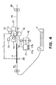
- Figures 4 , 5 and 6 show an Embodiment of the present invention.
- Figure 4 is a schematic illustration of an image forming apparatus according to this embodiment of the present invention.
- the same reference numerals as in the previous example are assigned to the elements having the corresponding functions in this embodiment, and the detailed description thereof is omitted for simplicity.
- control means 17 is provided with a switching means 17b.
- the control means 17 selectively effects, by switching means 17b a first mode in which the voltage is changed from VO to Vp and further to Vh similarly to Embodiment 1 ( Figure 6 ) and a second mode in which the voltage is maintained at Vp without providing Vh.
- the switching between the first mode and the second mode is carried out by the user.
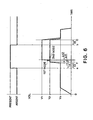
- the control means 17 activates the high voltage source 16 and effects the control such that current flowing through the current detecting means 18 is at a predetermined level.
- the timing at which the recording material sensor 20 detects the sheet (presence of the recording material), is indicated by time an in Figure 6 .
- t3 is set to be the time prior to the recording material P is nipped by the transfer nip T, more particularly, it is set to satisfy t3 ⁇ L/S where L is a distance between the recording material sensor 20 and the transfer nip T, and S is a feeding speed of the recording material.
- the control means 17 controls the high voltage source 16 so as to produce the voltage Vh (S5, S6) t4 after the timing of the detection of the presence of the sheet by the recording material sensor 20.
- the t4 is selected such that recording material P is nipped in the transfer nip T, that is, t4 satisfies t4 ⁇ L/S.
- the voltage Vp setting is maintained. Thereafter, when the recording material sensor 20 detects the absence of the sheet (t5 thereafter), control means 17 controls the high voltage source 16 to set the output voltage at VO, and the voltage supply is stopped at the end of the printing (S7, S8).
- a switching means for switching between the first mode and the second mode in the case of the material of the sheet which does not require a very high-voltage for the transfer of the toner image from the photosensitive drum 11 onto the recording material, the voltage is not said at a very high-voltage, by which soul-called toner scattering (if the voltage is too high, the toner jumps vigorously at the recording material, with the result of the toner scattering), can be avoided.
- this embodiment of the present invention is advantageous in that prop operations can be effected for various kinds of the recording materials.
- the switching means is actuated by the user.
- the kinds of the recording materials are automatically discriminated, and in response to the discrimination, the switching means may be automatically actuated.
- the reference signal providing a reference for the timing of switching the voltages Vp, Vh is determined using the recording material sensor disposed upstream of the transfer nip. This is not inevitable, and the reference signal may be the sheet feeding start signal or the rotation start signal of the registration roller after the sheet feeding. The same effects can be provided if the switching timing is determined on the basis of the time having elapsed from the start of the recording material feeding. If the position of the recording material is known, the reference signal may be the print start signal.
- the voltages Vp, Vh are determined by a linear equation. This is not inevitable, and another determination is usable if VO ⁇ Vp ⁇ Vh is satisfied.
- the damage of the image bearing member attributable to application of high voltage to the image bearing member when there is no recording material in the transfer nip can be avoided. Additionally, the voltage can be quickly raised to a high voltage, so that so-called transfer void attributable to the delay of the rising of the voltage can be avoided.
- an image forming apparatus including an image bearing member; a transferring member for transferring a toner image from the image bearing member onto a recording material at a transfer portion; voltage applying means for applying a voltage to the transferring member; wherein the voltage applying means is operable in a first mode and a second mode for applying to the transferring member a specific time sequence of voltages; and switching means for switching between the first mode and the second mode.
Landscapes
- Physics & Mathematics (AREA)
- General Physics & Mathematics (AREA)
- Electrostatic Charge, Transfer And Separation In Electrography (AREA)
- Control Or Security For Electrophotography (AREA)
Applications Claiming Priority (4)
| Application Number | Priority Date | Filing Date | Title |
|---|---|---|---|
| JP2000331173 | 2000-10-30 | ||
| JP2000331173 | 2000-10-30 | ||
| JP2001322652 | 2001-10-19 | ||
| JP2001322652A JP3862543B2 (ja) | 2000-10-30 | 2001-10-19 | 画像形成装置 |
Publications (3)
| Publication Number | Publication Date |
|---|---|
| EP1202130A2 EP1202130A2 (en) | 2002-05-02 |
| EP1202130A3 EP1202130A3 (en) | 2006-11-02 |
| EP1202130B1 true EP1202130B1 (en) | 2011-01-12 |
Family
ID=26603071
Family Applications (1)
| Application Number | Title | Priority Date | Filing Date |
|---|---|---|---|
| EP01125796A Expired - Lifetime EP1202130B1 (en) | 2000-10-30 | 2001-10-29 | Image forming apparatus |
Country Status (4)
| Country | Link |
|---|---|
| US (1) | US6654570B2 (enExample) |
| EP (1) | EP1202130B1 (enExample) |
| JP (1) | JP3862543B2 (enExample) |
| DE (1) | DE60143834D1 (enExample) |
Families Citing this family (14)
| Publication number | Priority date | Publication date | Assignee | Title |
|---|---|---|---|---|
| JP3707442B2 (ja) * | 2002-03-28 | 2005-10-19 | ブラザー工業株式会社 | 画像形成装置 |
| JP4250373B2 (ja) * | 2002-04-17 | 2009-04-08 | キヤノン株式会社 | 画像形成装置 |
| US6859631B2 (en) * | 2002-08-30 | 2005-02-22 | Canon Kabushiki Kaisha | Image forming apparatus and image forming method |
| US7031624B2 (en) * | 2002-10-21 | 2006-04-18 | Canon Kabushiki Kaisha | Image formation apparatus for providing a predetermined temperature lowering period in which the temperature of a fixing unit is reduced |
| US6965742B2 (en) * | 2002-11-08 | 2005-11-15 | Canon Kabushiki Kaisha | Image forming apparatus |
| US7050751B2 (en) * | 2003-07-28 | 2006-05-23 | Canon Kabushiki Kaisha | Image forming system with temporary storage trays between sheet storage units and image forming apparatus |
| JP2005075525A (ja) * | 2003-08-29 | 2005-03-24 | Canon Inc | シート材給送装置、および記録装置 |
| JP4217566B2 (ja) | 2003-09-01 | 2009-02-04 | キヤノン株式会社 | シート処理装置および画像形成装置 |
| JP4250581B2 (ja) * | 2004-09-29 | 2009-04-08 | キヤノン株式会社 | 画像形成装置 |
| JP4595683B2 (ja) * | 2005-05-31 | 2010-12-08 | 富士ゼロックス株式会社 | 画像形成装置 |
| JP2008129548A (ja) * | 2006-11-24 | 2008-06-05 | Canon Inc | 画像形成装置 |
| US20080145080A1 (en) * | 2006-12-14 | 2008-06-19 | William Paul Cook | Inter-Page Belt Impedance Measurement |
| US8238769B2 (en) * | 2009-12-08 | 2012-08-07 | Xerox Corporation | Electrostatic disturbance used in a timing routine for HVPS switching in a pressure transfer system involving BTB or BTR |
| JP7071133B2 (ja) * | 2018-01-19 | 2022-05-18 | キヤノン株式会社 | 画像形成装置 |
Family Cites Families (11)
| Publication number | Priority date | Publication date | Assignee | Title |
|---|---|---|---|---|
| US5179397A (en) * | 1989-04-03 | 1993-01-12 | Canon Kabushiki Kaisha | Image forming apparatus with constant voltage and constant current control |
| US5012293A (en) * | 1989-08-24 | 1991-04-30 | International Business Machines Corporation | Transfer station control in an electrophotographic reproduction device |
| JPH09134078A (ja) * | 1995-11-07 | 1997-05-20 | Oki Data:Kk | 電子写真記録装置 |
| US5697015A (en) * | 1996-05-29 | 1997-12-09 | Lexmark International, Inc. | Electrophotographic apparatus and method for inhibiting charge over-transfer |
| KR100191203B1 (ko) * | 1997-03-14 | 1999-06-15 | 윤종용 | 전자사진 현상방식을 채용한 화상형성장치의 전사 바이어스 제어방법 |
| JPH1152761A (ja) * | 1997-07-29 | 1999-02-26 | Toshiba Corp | 画像形成装置 |
| JPH1165324A (ja) * | 1997-08-13 | 1999-03-05 | Oki Data:Kk | 電子写真式プリンタ |
| JP3368220B2 (ja) * | 1998-12-03 | 2003-01-20 | キヤノン株式会社 | 画像形成装置 |
| JP3554217B2 (ja) * | 1999-03-17 | 2004-08-18 | キヤノン株式会社 | 画像形成装置 |
| JP3569155B2 (ja) * | 1999-05-24 | 2004-09-22 | シャープ株式会社 | 画像形成装置 |
| JP2001201958A (ja) * | 2000-01-18 | 2001-07-27 | Murata Mach Ltd | 画像形成装置 |
-
2001
- 2001-10-19 JP JP2001322652A patent/JP3862543B2/ja not_active Expired - Fee Related
- 2001-10-29 DE DE60143834T patent/DE60143834D1/de not_active Expired - Lifetime
- 2001-10-29 EP EP01125796A patent/EP1202130B1/en not_active Expired - Lifetime
- 2001-10-30 US US09/984,358 patent/US6654570B2/en not_active Expired - Lifetime
Also Published As
| Publication number | Publication date |
|---|---|
| EP1202130A3 (en) | 2006-11-02 |
| US20020051647A1 (en) | 2002-05-02 |
| JP2002202672A (ja) | 2002-07-19 |
| JP3862543B2 (ja) | 2006-12-27 |
| US6654570B2 (en) | 2003-11-25 |
| DE60143834D1 (de) | 2011-02-24 |
| EP1202130A2 (en) | 2002-05-02 |
Similar Documents
| Publication | Publication Date | Title |
|---|---|---|
| EP1202130B1 (en) | Image forming apparatus | |
| US6965742B2 (en) | Image forming apparatus | |
| US5884121A (en) | Transfer bias control method for image forming apparatus using electrophotographic process | |
| US6205299B1 (en) | Image forming apparatus in which whether transfer member should be constant-current-controlled or constant-voltage-controlled is selected depending on thickness of transfer material | |
| US7403727B2 (en) | Image forming apparatus and density adjusting method thereof | |
| JP5538846B2 (ja) | 画像形成装置 | |
| JP5058649B2 (ja) | 定着器制御装置及び画像形成装置 | |
| JP2004170968A (ja) | 画像形成装置 | |
| JP2016128863A (ja) | 画像形成装置 | |
| JP2024046724A (ja) | 画像形成装置 | |
| EP0568829B1 (en) | Image forming apparatus | |
| JP4428966B2 (ja) | 画像形成装置 | |
| JP2001272863A (ja) | シートに加湿しながら同時に装置からの液体の漏洩を制御する装置、及びプリント装置 | |
| KR101079579B1 (ko) | 화상형성장치 및 그 화상형성방법 | |
| US8238775B2 (en) | Image heating apparatus | |
| JP6693129B2 (ja) | 画像形成装置 | |
| JP6482310B2 (ja) | 画像形成装置 | |
| JP2002156883A (ja) | 画像形成装置 | |
| JPH0980936A (ja) | 画像形成装置 | |
| JPH11212315A (ja) | 画像形成装置の画質補償装置 | |
| US6807385B2 (en) | Difference potential preventing image forming apparatus | |
| JP7225992B2 (ja) | 画像形成装置 | |
| JP2000181249A (ja) | 画像形成装置 | |
| JPH05181335A (ja) | 画像形成装置 | |
| JPH0830108A (ja) | 画像形成装置 |
Legal Events
| Date | Code | Title | Description |
|---|---|---|---|
| PUAI | Public reference made under article 153(3) epc to a published international application that has entered the european phase |
Free format text: ORIGINAL CODE: 0009012 |
|
| 17P | Request for examination filed |
Effective date: 20011029 |
|
| AK | Designated contracting states |
Kind code of ref document: A2 Designated state(s): AT BE CH CY DE DK ES FI FR GB GR IE IT LI LU MC NL PT SE TR |
|
| AX | Request for extension of the european patent |
Free format text: AL;LT;LV;MK;RO;SI |
|
| PUAL | Search report despatched |
Free format text: ORIGINAL CODE: 0009013 |
|
| AK | Designated contracting states |
Kind code of ref document: A3 Designated state(s): AT BE CH CY DE DK ES FI FR GB GR IE IT LI LU MC NL PT SE TR |
|
| AX | Request for extension of the european patent |
Extension state: AL LT LV MK RO SI |
|
| AKX | Designation fees paid |
Designated state(s): DE FR GB IT |
|
| 17Q | First examination report despatched |
Effective date: 20080502 |
|
| GRAP | Despatch of communication of intention to grant a patent |
Free format text: ORIGINAL CODE: EPIDOSNIGR1 |
|
| GRAS | Grant fee paid |
Free format text: ORIGINAL CODE: EPIDOSNIGR3 |
|
| GRAA | (expected) grant |
Free format text: ORIGINAL CODE: 0009210 |
|
| AK | Designated contracting states |
Kind code of ref document: B1 Designated state(s): DE FR GB IT |
|
| REG | Reference to a national code |
Ref country code: GB Ref legal event code: FG4D |
|
| REF | Corresponds to: |
Ref document number: 60143834 Country of ref document: DE Date of ref document: 20110224 Kind code of ref document: P |
|
| REG | Reference to a national code |
Ref country code: DE Ref legal event code: R096 Ref document number: 60143834 Country of ref document: DE Effective date: 20110224 |
|
| PLBE | No opposition filed within time limit |
Free format text: ORIGINAL CODE: 0009261 |
|
| STAA | Information on the status of an ep patent application or granted ep patent |
Free format text: STATUS: NO OPPOSITION FILED WITHIN TIME LIMIT |
|
| 26N | No opposition filed |
Effective date: 20111013 |
|
| REG | Reference to a national code |
Ref country code: DE Ref legal event code: R097 Ref document number: 60143834 Country of ref document: DE Effective date: 20111013 |
|
| PGFP | Annual fee paid to national office [announced via postgrant information from national office to epo] |
Ref country code: FR Payment date: 20141027 Year of fee payment: 14 |
|
| PGFP | Annual fee paid to national office [announced via postgrant information from national office to epo] |
Ref country code: IT Payment date: 20141014 Year of fee payment: 14 |
|
| PG25 | Lapsed in a contracting state [announced via postgrant information from national office to epo] |
Ref country code: IT Free format text: LAPSE BECAUSE OF NON-PAYMENT OF DUE FEES Effective date: 20151029 |
|
| REG | Reference to a national code |
Ref country code: FR Ref legal event code: ST Effective date: 20160630 |
|
| PG25 | Lapsed in a contracting state [announced via postgrant information from national office to epo] |
Ref country code: FR Free format text: LAPSE BECAUSE OF NON-PAYMENT OF DUE FEES Effective date: 20151102 |
|
| PGFP | Annual fee paid to national office [announced via postgrant information from national office to epo] |
Ref country code: GB Payment date: 20171101 Year of fee payment: 17 |
|
| PGFP | Annual fee paid to national office [announced via postgrant information from national office to epo] |
Ref country code: DE Payment date: 20171229 Year of fee payment: 17 |
|
| REG | Reference to a national code |
Ref country code: DE Ref legal event code: R119 Ref document number: 60143834 Country of ref document: DE |
|
| GBPC | Gb: european patent ceased through non-payment of renewal fee |
Effective date: 20181029 |
|
| PG25 | Lapsed in a contracting state [announced via postgrant information from national office to epo] |
Ref country code: DE Free format text: LAPSE BECAUSE OF NON-PAYMENT OF DUE FEES Effective date: 20190501 |
|
| PG25 | Lapsed in a contracting state [announced via postgrant information from national office to epo] |
Ref country code: GB Free format text: LAPSE BECAUSE OF NON-PAYMENT OF DUE FEES Effective date: 20181029 |