EP1197000B1 - Ladder switch circuit for dac - Google Patents
Ladder switch circuit for dacInfo
- Publication number
- EP1197000B1 EP1197000B1 EP00932569A EP00932569A EP1197000B1 EP 1197000 B1 EP1197000 B1 EP 1197000B1 EP 00932569 A EP00932569 A EP 00932569A EP 00932569 A EP00932569 A EP 00932569A EP 1197000 B1 EP1197000 B1 EP 1197000B1
- Authority
- EP
- European Patent Office
- Prior art keywords
- resistance
- circuit
- resistor
- coupled
- bridge
- Prior art date
- Legal status (The legal status is an assumption and is not a legal conclusion. Google has not performed a legal analysis and makes no representation as to the accuracy of the status listed.)
- Expired - Lifetime
Links
- 239000004020 conductor Substances 0.000 claims description 54
- 239000002131 composite material Substances 0.000 claims description 6
- 230000001419 dependent effect Effects 0.000 claims description 5
- 230000000295 complement effect Effects 0.000 claims description 2
- 230000008878 coupling Effects 0.000 claims 2
- 238000010168 coupling process Methods 0.000 claims 2
- 238000005859 coupling reaction Methods 0.000 claims 2
- 239000000872 buffer Substances 0.000 description 7
- 230000007423 decrease Effects 0.000 description 3
- 239000000463 material Substances 0.000 description 3
- 239000010409 thin film Substances 0.000 description 3
- 238000010586 diagram Methods 0.000 description 2
- 238000000034 method Methods 0.000 description 2
- 238000006243 chemical reaction Methods 0.000 description 1
- 229910021357 chromium silicide Inorganic materials 0.000 description 1
- QKJXFFMKZPQALO-UHFFFAOYSA-N chromium;iron;methane;silicon Chemical compound C.[Si].[Cr].[Fe] QKJXFFMKZPQALO-UHFFFAOYSA-N 0.000 description 1
Images
Classifications
-
- H—ELECTRICITY
- H03—ELECTRONIC CIRCUITRY
- H03M—CODING; DECODING; CODE CONVERSION IN GENERAL
- H03M1/00—Analogue/digital conversion; Digital/analogue conversion
- H03M1/06—Continuously compensating for, or preventing, undesired influence of physical parameters
- H03M1/08—Continuously compensating for, or preventing, undesired influence of physical parameters of noise
- H03M1/089—Continuously compensating for, or preventing, undesired influence of physical parameters of noise of temperature variations
-
- H—ELECTRICITY
- H03—ELECTRONIC CIRCUITRY
- H03M—CODING; DECODING; CODE CONVERSION IN GENERAL
- H03M1/00—Analogue/digital conversion; Digital/analogue conversion
- H03M1/66—Digital/analogue converters
- H03M1/74—Simultaneous conversion
- H03M1/78—Simultaneous conversion using ladder network
- H03M1/785—Simultaneous conversion using ladder network using resistors, i.e. R-2R ladders
Definitions
- the invention relates to bit switch circuitry associated with R/2R ladder voltage divider networks used in digital to analog converters (DACs).
- DACs digital to analog converters
- US 5,764,174 discloses a switch architecture for digital-to-analog converters including a R/2R ladder with a control circuit generating a gate voltage for a first and a second MOSFET switch.
- Figs. 5 and 9 of US 5,764,174 (Dempscy et a.), in which V cd and V cn of Fig. 9 are provided as controlled "supply" voltages to CMOS buffers 116i and 118i of Fig. 5.
- US 5,075,677 (Meaney et al.) and US 4,558,242 (Tuthill et al.) also disclose prior art circuits for switching the 2R shunt resistors of R/2R ladders to high and low reference voltages.
- the control circuit of Fig. 9 of the Dempsey et al. patent generates two control voltages V cd and V cn which are applied as supply voltages for a pair of CMOS inverters or buffers 46 i and 48 i , respectively.
- the CMOS buffers 46 i and 48 i are controlled by a binary input b i to turn MOSFETs 42 i and 44 i on and off.
- the drain electrodes of MOSFETs 42 i and 44 i are connected to a corresponding leg of an R/2R ladder network.
- MOSFET 42 i can be either P-channel or N-channel (See Fig. 6 of the Dempsey et al. patent), and buffer 46; is correspondingly inverting or non-inverting.
- the operational amplifiers 58 and 59 each operate to balance their (+) and (-) inputs.
- Resistors 54 and 57 in Fig. 9 of the Dempsey et al. patent establish the same bias currents, in order to match the on resistance of combined MOSFETs 55 to the resistance of combined resistors 52, and match the on resistance of combined MOSFETs 56 to the resistance of combined resistors 53.
- the circuit structure which produces the common bias currents includes resistors 54 and 57 and prevents accurate operation of the circuit of Fig. 9 of the Dempsey et al. patent if V REF- is not more than approximately 2 volts above V REF- . As the difference between V REF- and V REF- decreases, the current through the circuit of Fig. 9 decreases, and the offset errors of the two operational amplifiers become increasingly large proportions of the voltage drops across the resistors. This leads to increasingly large inaccuracies in operation.
- Fig. 11 of the Dempsey et al. patent discloses an alternative embodiment in which unit resistors 72 and 74 are connected in series between the drains of the MOSFET switches 42 i and 44 i and the corresponding leg of the R/2R ladder. This embodiment controls the on resistance of the MOSFET switches 42 i and 44 i with respect to the resistances of unit resistors 72 and 74.
- control and switching circuitry of the Dempsey et al. patent and all of the relevant prior art is designed to be used in conjunction with conventional R/2R resistive divider networks in which the series resistors all have the resistance R and the shunt resistors all have the resistance 2R.
- Very large MOSFETs are required to provide a 40 ohm on resistance because the channel width W must be very large.
- Very large MOSFETs are also required to provide an on resistance of 320 kilohms to 1.20 megohms because the channel length L must be very large. Therefore, a large amount of chip area is required for an accurate implementation of a digital-to-analog converter using an R/2R divider network. To avoid the large amount of chip area, those skilled in the art have developed various "short cuts" for avoiding the use of very large MOSFET switches for the LSB bits, but these techniques introduce inaccuracies that may not be acceptable for digital-to-analog converters having more than about 12 bits of resolution.
- a difficulty in scaling MOSFET switches to have large on resistances by making the channel length L very long is that the magnitude of the effective gate-to-source voltage which produces the on resistance R ON is progressively reduced along the length of the channel region due to a voltage drop developed along the channel region due to current flowing through it. Consequently, binarily scaling the W/L ratio does not result in binarily scaling R ON for all values of channel current.
- the invention provides a circuit for switching a shunt resistor with the features of claim 1 with which the before mentioned problems are avoided.
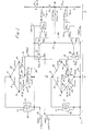
- a 16-bit digital-to-analog converter 1 includes a resistive divider network 10 having a plurality of series resistors 27 i of resistance R and a plurality of shunt resistors 30; each having a resistance 2R', 20 switch and driver circuits 34 i , and first and second bridge control circuits 11 and 12, wherein i has values from 1 to 20.
- Lower bridge control circuit 11 applies an externally supplied reference voltage V REFL to each of 16 N-channel V REFL switch MOSFETs 44 i
- upper bridge control circuit 12 applies an externally supplied reference voltage V REFH to each of i N-channel "V REFH switch" MOSFETs 42 i . Except for the first three most significant bits, switch MOSFETs 42 i and 44 i in each switch and driver circuit 34 i are turned on and off in response to the corresponding ith bit DIN i of a 16-bit digital input word.
- the first three bits 1-3 of the digital input code are "segmented" or decoded in a thermometer type decoder with three inputs and seven outputs going to each of the first seven segments of the resistive network ladder circuit, as described subsequently with reference to Fig. 2. This produces outputs for all eight combinations of the first three most significant bits of the digital input word, each separated from another by one-eighth of the voltage range determined by the difference between V REFL and V REFH .)
- switch MOSFET 42 i is connected to a conductor 33 on which the voltage V REFH (typically +10 volts, but it could be as low as about -9.9 volts when V REFL is -10 volts) is maintained.
- the source of switch MOSFET 42 i is connected by conductor 31 to shunt resistor 30 i of a "modified R/2R ladder network" 10.
- Switch MOSFET 44 i has its drain connected by conductor 31 to shunt resistor 30 i and its source connected to conductor 40, on which V REFL is provided by the user of digital-to-analog converter 1.
- V REFL has a value of typically -10 volts, but it could be as high as +9.9 volts when V REFH is +10 volts.
- the circuit of Fig. 1 provides very accurate values of R ON of switch MOSFETs 42 i and 44 i despite changes in V REFH and V REFL , even when the two are very close (e.g., within 100 millivolts) in value.
- R/2R' ladder network 10 differs from a conventional R/2R ladder network (e.g., as shown in Fig. 13 of the Dempsey et al. patent) because the resistance of shunt resistor 30 i is not 2R as in a conventional R/2R ladder, but instead is equal to 2R', where 2R' is equal to 2R-R ONi , R ONi being the channel resistance of the one of switch MOSFETs 42 i and 44 i that is presently on.
- the total resistance "2R" of each shunt resistance of the resistive divider network of the present invention includes the on resistance R ONi of the corresponding bit switch 42 i or 44 i , unlike the prior art digital-to-analog converters in which each shunt leg of the resistive network 10 has a value of precisely 2R.
- the W/L ratios (i.e., the channel-width-to-channel-length ratios) of the switch MOSFETs 44 i and 42 i of the various bits are not adjusted to provide binarily scaled on resistances. Instead, they are selected to be of suitable small sizes and to have suitable on resistances.
- the value of the various 2R' resistances of R/2R' ladder network 10 can be different for the various bits; this feature is different from a conventional R/2R ladder network wherein the 2R resistances of all shunt resistors of the resistive divider network necessarily are precisely equal to a value of 2R.
- All of the resistors in bridge control circuits 11 and 12 and R/2R' divider network 10 are thin film resistors formed of chromium silicide or silicon chrome material, referred to as sichrome, so the temperature coefficient of the on resistance of MOSFET 24 tracks with the temperature coefficient of the resistance of reference resistor 26 and the on resistance of MOSFET 23 tracks with the resistance of a second reference resistor 25. Consequently, the temperature coefficients of the on resistances of switch MOSFETs 44 i also track with the temperature coefficient of the resistance of sichrome resistor 26 and the sichrome resistors R and 2R' of divider network 10.
- Lower bridge control circuit 11 includes a bridge circuit 11A including a first reference resistor 26 of resistance R REF1 having its lower terminal coupled to conductor 40 and its upper terminal coupled to one terminal of a resistor 46'.
- the other terminal of resistor 46' is connected by a conductor 13 to the (-) input of an operational amplifier 37 and to the lower terminal of a resistor 35.
- the upper terminal of resistor 35 is connected by conductor 15 to the (+) terminal of a constant voltage source circuit 51 having a value of approximately 2 volts and to the upper terminal of a resistor 36.
- the voltage on conductor 15 is "bootstrapped" up to a level 2 volts above V REFL , since the (-) terminal of constant voltage source 51 is connected to V REFL conductor 40.
- Constant voltage circuit 51 is included in a constant voltage source 50 that typically is connected between a +15 volt power supply +V and V REFL .
- the lower terminal of resistor 36 is connected by conductor 14 to the (+) input of operational amplifier 37 and is coupled by a resistor 46 to the drain of an N-channel reference transistor 24 having its gate connected to the output of operational amplifier 37 by conductor 38.
- the source of N-channel reference MOSFET 24 is connected to conductor 40 on which the external reference voltage V REFL is provided.
- a voltage V REGL is produced by operational amplifier 37 on conductor 38, wherein operational amplifier 37 operates as a servo amplifier to establish the gate voltage of control MOSFET 24 as needed to cause its on resistance to be equal to R REF1 , and to provide the same gate voltage to switch MOSFET 44 i so its on resistance R ONi is equal to or scaled with respect to R REF1 , according to the W/L ratio thereof.
- V REGL is connected to the high supply terminal of a CMOS inverter 39, the low supply voltage terminal of which is connected to a negative supply voltage (which typically is -15 volts). Consequently, the high output voltage of CMOS inverter 39 will be equal to V REGL .
- CMOS inverter 39 The output of CMOS inverter 39 is connected to the gate of switch MOSFET 44 i .
- Resistors 46 and 46' perform the function of providing more "head room” for operational amplifier 37. That is, the currents flowing through resistors 46 and 46' develop equal voltage drops across them that shift the voltages on conductors 13 and 14 to higher levels relative to the voltage on conductor 40. This provides more "operating room” or "head room” for the input stage of operational amplifier 37.
- Resistor 46' actually is integral with reference resistor 26 in a single 27.0 kilohm resistor 26,46'; resistor 46' is illustrated as a separate resistor to aid in explanation of the invention.
- upper bridge control circuit 12 includes a bridge circuit 12A with a similar second reference resistor 25 of resistance R REF2 .
- Reference resistor 25 has its lower terminal connected to conductor 33, on which a second external reference voltage V REFH of typically +10 volts is provided by the user of digital-to-analog converter 1.
- the upper terminal of reference resistor 25 is coupled by a resistor 54' to the (-) input of operational amplifier 43 and to the lower terminal of a resistor 41.
- the upper terminal of resistor 41 is connected to the upper terminal of a resistor 55 and to the (+) terminal of a constant voltage supply circuit 52 bootstrapped to a value 2 volts higher than V REFH . This produces a voltage of approximately 2 volts across the upper bridge circuit 12A.
- the (-) terminal of constant voltage source circuit 52 is connected to conductor 33.
- the lower terminal of resistor 55 is connected by conductor 49 to the (+) input of operational amplifier 43 and is coupled by a resistor 54 to the drain of a second reference N-channel MOSFET 23, the gate of which is connected by conductor 56 to the output of operational amplifier 43.
- the bootstrapped voltage sources 51 and 52 each include a conventional constant current source connected to supply a constant current through resistive elements and/or diode elements across which the 2 volt voltage drops are developed.
- Operational amplifier 43 produces a reference voltage V REGH on conductor 56, wherein operational amplifier 43 operates as a servo amplifier to establish the gate voltage of control MOSFET 23 as needed to cause its on resistance to be equal to R REF2 , and to provide the same gate voltage to switch MOSFET 42 i so its on resistance R ONi is equal to or scaled with respect to R REF2 , according to the W/L ratio thereof.
- V REGH is connected to the high supply voltage terminal of a CMOS inverter 21. Consequently, the high output voltage of CMOS inverter 21 will be equal to V REGH .
- the low supply voltage terminal of CMOS inverter 45 is connected to -15 volts.
- the source of reference MOSFET 23 is connected to conductor 33.
- Resistors 54 and 54' perform the function of providing more head room for operational amplifier 43. That is, the currents flowing through resistors 54' and 46' develop voltage drops across them that shift the voltages on conductors 48 and 49 to higher levels relative to the voltage on conductor 33. This provides more "operating room” or "head room” for the input stage of operational amplifier 43.
- resistor 54' actually is integral with reference resistor 25 in a single 13.5 kilohm resistor 25,54'; again, resistor 54' is shown as a separate resistor to aid in explanation of the invention.
- the resistance R REF1 of reference resistor 26 of lower bridge circuit 11A is scaled relative to reference resistor 25 in bridge circuit 12A in order to reduce power dissipation in lower bridge circuit 11A.
- R REF1 can be 2.4 kilohms, which can be twice the 1.2 kilohm resistance R REF2 of reference resistor 25 in upper bridge circuit 12A.
- the nominal values of resistors 35 and 36 of lower bridge control circuit 11 are 23 kilohms and 11.5 kilohms, respectively, and the resistances of resistors 41 and 55 of upper bridge control circuit 12 are both 11.5 kilohms.
- the ratio of resistances of resistors 46' and 46 is equal to 2, and the ratio of resistances of resistors 35 and 36 also is equal to 2.
- Resistor 35, resistor 46', and reference resistor 26 of bridge 11A form a voltage divider that applies a voltage via conductor 13 to the (-) input of operational amplifier 37.
- Resistor 36, resistor 46, and reference MOSFET 24 form a voltage divider that applies a voltage via conductor 14 to the (+) input of operational amplifier 37.
- Operational amplifier 37 applies a voltage via conductor 38 to adjust the channel resistance R ON of MOSFET 24 so that the voltage on conductor 14 equals the voltage on conductor 13.
- resistors 54 and 54' are equal, not scaled, and the resistances of resistors 41 and 55 also are equal.
- Resistor 41, resistor 54', and reference resistor 25 of bridge control circuit 12A form a voltage divider that applies a voltage via conductor 48 to the (+) input of operational amplifier 43.
- Resistor 55, resistor 54, and reference MOSFET 23 form a voltage divider that applies a voltage via conductor 49 to the (-) input of operational amplifier 43.
- Operational amplifier 43 applies a voltage via conductor 56 to adjust the channel resistance R ON of reference MOSFET 23 so that the voltage on conductor 49 equals the voltage on conductor 48. This occurs when the R ON resistance of MOSFET 23 equals R REF2 .
- the same voltage V REGH needed to cause the R ON resistance of MOSFET 23 to be equal to R REF2 also is applied by conductor 56 and CMOS inverter 21 to the gate of MOSFET 42 i , causing the channel resistance of MOSFET 42 i to be equal to R REF2 or to be suitably scaled with respect to R REF2 .
- the on resistances of switch MOSFETs 44 i and 42 i are equal to (or scaled to) different resistance values.
- any of the resistors can be regarded as a "reference resistor” with respect to which the on resistances of the corresponding MOSFETs 44 i and 42 i are controlled.
- the various node voltages and branch currents in bridge circuits 11A and 12A can be considered to be a "reference value" with respect to which the on resistances of corresponding switch MOSFETs 44 i or 42 i are controlled.
- the above described ratioing of the corresponding resistances in the left side and right side of bridge circuit 11A of lower bridge control circuit 11 decreases the bias current therein. This substantially reduces the otherwise higher power dissipation in lower bridge control circuit 11.
- the power dissipation in lower bridge control circuit 11 is equal to the bias current therein multiplied by the large voltage difference between the +15 volt supply voltage applied to constant voltage source circuit 50 and V REFL , which is typically -10 volts.
- R/2R' ladder network (rather than an R/R2 ladder network) in digital-to-analog converter 1 is that the R ONi switch resistances have precisely the same temperature coefficients as the 2R' resistances of the R/2R' ladder network.
- the reference resistors 26,46' and 25,54' must be composed of the same material (e.g., sichrome) of which the ladder network resistors are composed. Note that this is not the case for the prior art R/2R ladder network and MOSFET switch control circuits, including those disclosed in the above mentioned Dempsey et al. patent.
- transistors 23 and 24 are controlled by operational amplifiers 43 and 37, respectively, to precisely match R REF2 and R REF1, respectively, which are "hidden" portions of a larger resistors that include resistors 54' and 46', respectively.
- operational amplifier 58 operates to precisely match the composite resistance of transistors 55 with the composite resistance 52.
- the resistances of the left hand legs 35 and 46',26 are scaled relative to the resistances of the right hand legs 36,24 in order to reduce current and hence power dissipation.
- FIG. 1 shows two additional switch and driver circuits 34 i-1 and 34 i+1 on either side of the above described switch and driver circuit 34 i .
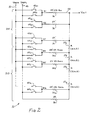
- the remainder of divider network 10 is shown in Fig. 2.
- resistive divider network 10 includes a first section 10A having seven equal segments S1,2...7 in which the most significant three bits of the digital input word constitute a thermometer code that is decoded to provide eight equal voltage segments for implementation of the three most significant bits (bits 1-3) of digital-to-analog converter 1.
- the conductor 58 connected to the right end of each of the 2R' shunt resistors 30 of seven-segment section 10A conducts the output voltage V OUT of digital-to-analog converter 1.
- Each shunt leg in Fig. 2 can have a resistance of 100 kilohms, including the resistance 2R' and the R ON of the associated switches.
- Resistive divider 10 also includes a second section 10B including an R/2R' ladder network for bits 4-16, wherein each series resistor 27 4,5...15 has a value R.
- Each shunt resistor 30 4,5...16 has a value 2R' equal to 2R-R ONi , where R ONi is the on resistance of the corresponding switches 42 i and 44 i .
- the seven segment resistors 2R' of sections S1-S7 are equal (for example) to 100 kilohms which include the on resistances of MOSFET switches 42 S1-7 and 44 S1-7 , which can be 75 ohms.
- the resistances of the on resistances switches for bit B4 can be 150 ohms.
- the on resistances for the switches for bits B5-9 can be 300 ohms.
- the on resistances for bits B10-16 can be 600 ohms. Note that these on resistances are arbitrary, The low values of the on resistances allow use of MOSFET switches all with the same short channel length, with relatively little of the previously described code-dependent variation in R ON .
- a main advantage of digital-to-analog converter 1 as described above is that the on resistances of the switch MOSFETs 42 i and 44, do not have to be binarily scaled, and therefore can be much smaller in size than the MSB switch MOSFETs and LSB switch MOSFETs of the prior art.
- This advantage is due to the described circuit in which the on resistance of control MOSFETs 23 and 24 tracks with reference resistors composed of the same material as the resistors of divider network 10. 16-bit and higher resolution and corresponding accuracy can be achieved without resort to any of the above mentioned "short cut" techniques which have been used previously to avoid use of very large switch transistors that would be required for accurate implementation of the least significant bits of the digital-to-analog converter.
- the independence of the bridge control circuits 11 and 12 allows ratioing of their bias currents so that the current through lower bridge control circuit 11 is substantially less than that through upper bridge control circuit 12.
- the greatly reduced size of the switch MOSFETs 42 i and 44 i for the most significant and least significant groups of bits of digital-to-analog convener 1 also results in reduced chip size and reduced cost.
- the independence of upper and lower bridge control circuits 11 and 12 allows the difference between the externally supplied reference voltages to be small.
- bridge circuit 11A could be replaced by a bridge circuit which is the mirror image of bridge circuit 12A and is shown below conductor 33, with the polarity of voltage source 52 reversed and N-channel MOSFET 23 replaced by an equivalent P-channel MOSFET. Or, an N-channel MOSFET 23 could be used, with its source and drain electrodes reversed and with the (+) and (-) inputs of operational amplifier 43 also reversed. Similarly, lower bridge circuit 11A could be replaced by a mirror image thereof.
Landscapes
- Engineering & Computer Science (AREA)
- Theoretical Computer Science (AREA)
- Analogue/Digital Conversion (AREA)
- Electronic Switches (AREA)
Applications Claiming Priority (3)
| Application Number | Priority Date | Filing Date | Title |
|---|---|---|---|
| US09/337,796 US6150971A (en) | 1999-06-22 | 1999-06-22 | R/2R' ladder switch circuit and method for digital-to-analog converter |
| US337796 | 1999-06-22 | ||
| PCT/US2000/013650 WO2000079685A1 (en) | 1999-06-22 | 2000-05-18 | Ladder switch circuit for dac |
Publications (3)
| Publication Number | Publication Date |
|---|---|
| EP1197000A1 EP1197000A1 (en) | 2002-04-17 |
| EP1197000A4 EP1197000A4 (en) | 2004-03-10 |
| EP1197000B1 true EP1197000B1 (en) | 2006-08-16 |
Family
ID=23322048
Family Applications (1)
| Application Number | Title | Priority Date | Filing Date |
|---|---|---|---|
| EP00932569A Expired - Lifetime EP1197000B1 (en) | 1999-06-22 | 2000-05-18 | Ladder switch circuit for dac |
Country Status (5)
| Country | Link |
|---|---|
| US (1) | US6150971A (enExample) |
| EP (1) | EP1197000B1 (enExample) |
| JP (1) | JP3749174B2 (enExample) |
| DE (1) | DE60030125T2 (enExample) |
| WO (1) | WO2000079685A1 (enExample) |
Families Citing this family (9)
| Publication number | Priority date | Publication date | Assignee | Title |
|---|---|---|---|---|
| US6720799B2 (en) * | 2001-01-11 | 2004-04-13 | Broadcom Corporation | Replica network for linearizing switched capacitor circuits |
| US7449783B2 (en) * | 2005-05-05 | 2008-11-11 | Texas Instruments Incorporated | Nonlinear via arrays for resistors to reduce systematic circuit offsets |
| US7425912B2 (en) * | 2006-06-23 | 2008-09-16 | Analog Devices, Inc. | Digital-to-analog converter with controlled buffered inputs |
| US8013772B2 (en) * | 2009-12-31 | 2011-09-06 | Texas Instruments Incorporated | Reduced area digital-to-analog converter |
| JP5546361B2 (ja) * | 2010-06-10 | 2014-07-09 | セイコーインスツル株式会社 | 可変抵抗回路を備えた半導体集積回路 |
| US10608489B2 (en) | 2012-12-11 | 2020-03-31 | Enedym Inc. | Switched reluctance machine with rotor excitation using permanent magnets |
| CN112203532A (zh) | 2018-05-31 | 2021-01-08 | 日本烟草产业株式会社 | 香味生成装置 |
| CN111431513B (zh) * | 2020-04-20 | 2024-09-20 | 深圳市智鼎驱动技术有限公司 | 一种新型电压选择保护电路 |
| US12170527B2 (en) * | 2021-06-28 | 2024-12-17 | Infinera Corporation | High linearity resistive digital-to-analog converters with dynamic control for temperature and voltage invariant on-resistance of switches |
Family Cites Families (13)
| Publication number | Priority date | Publication date | Assignee | Title |
|---|---|---|---|---|
| JPS5831617A (ja) * | 1981-08-20 | 1983-02-24 | Nec Corp | R−2rはしご形d−a変換器 |
| US4590456A (en) * | 1982-09-02 | 1986-05-20 | Analog Devices, Incorporated | Low leakage CMOS D/A converter |
| US4553132A (en) * | 1983-01-24 | 1985-11-12 | Rca Corporation | Apparatus for matching FET switches as for a video digital-to-analog converter |
| US4558242A (en) * | 1983-02-11 | 1985-12-10 | Analog Devices, Incorporated | Extended reference range, voltage-mode CMOS D/A converter |
| US4683458A (en) * | 1986-07-31 | 1987-07-28 | Robert Hallgren | Current-steering digital-to-analog converter for providing bi-directional currents through a load |
| US4800365A (en) * | 1987-06-15 | 1989-01-24 | Burr-Brown Corporation | CMOS digital-to-analog converter circuitry |
| JPH02246624A (ja) * | 1989-03-20 | 1990-10-02 | Yamaha Corp | バッファ回路 |
| US5075677A (en) * | 1989-07-27 | 1991-12-24 | Analog Devices, Inc. | Voltage-switching d/a converter using p- and n-channel MOSFETs |
| JPH0377430A (ja) * | 1989-08-19 | 1991-04-03 | Fujitsu Ltd | D/aコンバータ |
| US5387912A (en) * | 1993-12-02 | 1995-02-07 | Analog Devices, Inc. | Digital-to-analog converter with reference glitch reduction |
| US5684481A (en) * | 1994-03-18 | 1997-11-04 | Analog Devices | Rail-to-rail DAC drive circuit |
| US5668553A (en) * | 1995-11-27 | 1997-09-16 | Analog Devices, Inc. | R2R digital to analog converter with common shutdown mode |
| US5764174A (en) * | 1996-05-14 | 1998-06-09 | Analog Devices, Inc. | Switch architecture for R/2R digital to analog converters |
-
1999
- 1999-06-22 US US09/337,796 patent/US6150971A/en not_active Expired - Lifetime
-
2000
- 2000-05-18 WO PCT/US2000/013650 patent/WO2000079685A1/en not_active Ceased
- 2000-05-18 EP EP00932569A patent/EP1197000B1/en not_active Expired - Lifetime
- 2000-05-18 DE DE60030125T patent/DE60030125T2/de not_active Expired - Lifetime
- 2000-05-18 JP JP2001505139A patent/JP3749174B2/ja not_active Expired - Fee Related
Also Published As
| Publication number | Publication date |
|---|---|
| EP1197000A4 (en) | 2004-03-10 |
| WO2000079685A1 (en) | 2000-12-28 |
| DE60030125T2 (de) | 2007-02-22 |
| JP3749174B2 (ja) | 2006-02-22 |
| DE60030125D1 (de) | 2006-09-28 |
| US6150971A (en) | 2000-11-21 |
| JP2004515931A (ja) | 2004-05-27 |
| EP1197000A1 (en) | 2002-04-17 |
Similar Documents
| Publication | Publication Date | Title |
|---|---|---|
| US5495245A (en) | Digital-to-analog converter with segmented resistor string | |
| US5111205A (en) | Digital-to-analog and analog-to-digital converters | |
| JP3967774B2 (ja) | R/2rディジタル―アナログ変換器のための改良されたスイッチ・アーキテクチャ | |
| JP3779056B2 (ja) | 電圧発生回路、及び、d/a変換回路 | |
| US6522280B2 (en) | Adjustable digital-to-analog converter | |
| WO2001028102A1 (en) | Lsb interpolation circuit and method for segmented digital-to-analog converter | |
| EP1465347B1 (en) | Monotonic precise current DAC | |
| EP1197000B1 (en) | Ladder switch circuit for dac | |
| US4958155A (en) | Ultra fast digital-to-analog converter with independent bit current source calibration | |
| EP1098443B1 (en) | Digital-analog conversion circuit | |
| EP0378840A2 (en) | Digital to analog converter having single resistive string with shiftable voltage thereacross | |
| JP2552461B2 (ja) | デジタル−アナログ変換器 | |
| JP3246498B2 (ja) | ディジタル/アナログ変換器 | |
| US6252534B1 (en) | Resistor string DAC with current mode interpolation | |
| US4811017A (en) | Digital-to-analog converter | |
| JP2004515931A5 (enExample) | ||
| US7639168B1 (en) | Systems and methods for switch resistance control in digital to analog converters (DACs) | |
| JP3460765B2 (ja) | 電流加算型デジタルアナログ変換回路 | |
| JP3551200B2 (ja) | デジタル/アナログ変換回路 | |
| EP4513764A1 (en) | Digital-to-analog converter | |
| CN112398386A (zh) | 具有正弦数模转换器的马达步进驱动器 | |
| JPH0424892B2 (enExample) | ||
| JP2006197052A (ja) | 電流セルマトリクス型da変換器 | |
| JPH05327510A (ja) | 電圧加算方式d/aコンバータ | |
| JPH11261418A (ja) | アナログ/ディジタル変換器 |
Legal Events
| Date | Code | Title | Description |
|---|---|---|---|
| PUAI | Public reference made under article 153(3) epc to a published international application that has entered the european phase |
Free format text: ORIGINAL CODE: 0009012 |
|
| 17P | Request for examination filed |
Effective date: 20011214 |
|
| AK | Designated contracting states |
Kind code of ref document: A1 Designated state(s): AT BE CH CY DE DK ES FI FR GB GR IE IT LI LU MC NL PT SE |
|
| A4 | Supplementary search report drawn up and despatched |
Effective date: 20040127 |
|
| RIC1 | Information provided on ipc code assigned before grant |
Ipc: 7H 03M 1/06 B Ipc: 7H 03M 1/78 A |
|
| RBV | Designated contracting states (corrected) |
Designated state(s): DE FR GB IE IT NL |
|
| 17Q | First examination report despatched |
Effective date: 20050314 |
|
| GRAP | Despatch of communication of intention to grant a patent |
Free format text: ORIGINAL CODE: EPIDOSNIGR1 |
|
| GRAS | Grant fee paid |
Free format text: ORIGINAL CODE: EPIDOSNIGR3 |
|
| GRAA | (expected) grant |
Free format text: ORIGINAL CODE: 0009210 |
|
| AK | Designated contracting states |
Kind code of ref document: B1 Designated state(s): DE FR GB IE IT NL |
|
| PG25 | Lapsed in a contracting state [announced via postgrant information from national office to epo] |
Ref country code: IT Free format text: LAPSE BECAUSE OF FAILURE TO SUBMIT A TRANSLATION OF THE DESCRIPTION OR TO PAY THE FEE WITHIN THE PRESCRIBED TIME-LIMIT;WARNING: LAPSES OF ITALIAN PATENTS WITH EFFECTIVE DATE BEFORE 2007 MAY HAVE OCCURRED AT ANY TIME BEFORE 2007. THE CORRECT EFFECTIVE DATE MAY BE DIFFERENT FROM THE ONE RECORDED. Effective date: 20060816 Ref country code: NL Free format text: LAPSE BECAUSE OF FAILURE TO SUBMIT A TRANSLATION OF THE DESCRIPTION OR TO PAY THE FEE WITHIN THE PRESCRIBED TIME-LIMIT Effective date: 20060816 |
|
| REG | Reference to a national code |
Ref country code: GB Ref legal event code: FG4D |
|
| REG | Reference to a national code |
Ref country code: IE Ref legal event code: FG4D |
|
| REF | Corresponds to: |
Ref document number: 60030125 Country of ref document: DE Date of ref document: 20060928 Kind code of ref document: P |
|
| NLV1 | Nl: lapsed or annulled due to failure to fulfill the requirements of art. 29p and 29m of the patents act | ||
| ET | Fr: translation filed | ||
| PLBE | No opposition filed within time limit |
Free format text: ORIGINAL CODE: 0009261 |
|
| STAA | Information on the status of an ep patent application or granted ep patent |
Free format text: STATUS: NO OPPOSITION FILED WITHIN TIME LIMIT |
|
| 26N | No opposition filed |
Effective date: 20070518 |
|
| PG25 | Lapsed in a contracting state [announced via postgrant information from national office to epo] |
Ref country code: IE Free format text: LAPSE BECAUSE OF NON-PAYMENT OF DUE FEES Effective date: 20070518 |
|
| REG | Reference to a national code |
Ref country code: FR Ref legal event code: PLFP Year of fee payment: 16 |
|
| PGFP | Annual fee paid to national office [announced via postgrant information from national office to epo] |
Ref country code: DE Payment date: 20150601 Year of fee payment: 16 Ref country code: GB Payment date: 20150424 Year of fee payment: 16 |
|
| PGFP | Annual fee paid to national office [announced via postgrant information from national office to epo] |
Ref country code: FR Payment date: 20150424 Year of fee payment: 16 |
|
| REG | Reference to a national code |
Ref country code: DE Ref legal event code: R119 Ref document number: 60030125 Country of ref document: DE |
|
| GBPC | Gb: european patent ceased through non-payment of renewal fee |
Effective date: 20160518 |
|
| REG | Reference to a national code |
Ref country code: FR Ref legal event code: ST Effective date: 20170131 |
|
| PG25 | Lapsed in a contracting state [announced via postgrant information from national office to epo] |
Ref country code: DE Free format text: LAPSE BECAUSE OF NON-PAYMENT OF DUE FEES Effective date: 20161201 Ref country code: FR Free format text: LAPSE BECAUSE OF NON-PAYMENT OF DUE FEES Effective date: 20160531 |
|
| PG25 | Lapsed in a contracting state [announced via postgrant information from national office to epo] |
Ref country code: GB Free format text: LAPSE BECAUSE OF NON-PAYMENT OF DUE FEES Effective date: 20160518 |