EP1187455A2 - Bilddatenverarbeitungsvorrichtung und elektronische Kamera - Google Patents
Bilddatenverarbeitungsvorrichtung und elektronische Kamera Download PDFInfo
- Publication number
- EP1187455A2 EP1187455A2 EP01307532A EP01307532A EP1187455A2 EP 1187455 A2 EP1187455 A2 EP 1187455A2 EP 01307532 A EP01307532 A EP 01307532A EP 01307532 A EP01307532 A EP 01307532A EP 1187455 A2 EP1187455 A2 EP 1187455A2
- Authority
- EP
- European Patent Office
- Prior art keywords
- data size
- image data
- color
- data
- image
- Prior art date
- Legal status (The legal status is an assumption and is not a legal conclusion. Google has not performed a legal analysis and makes no representation as to the accuracy of the status listed.)
- Granted
Links
Images


Classifications
-
- H—ELECTRICITY
- H04—ELECTRIC COMMUNICATION TECHNIQUE
- H04N—PICTORIAL COMMUNICATION, e.g. TELEVISION
- H04N23/00—Cameras or camera modules comprising electronic image sensors; Control thereof
-
- G—PHYSICS
- G06—COMPUTING; CALCULATING OR COUNTING
- G06T—IMAGE DATA PROCESSING OR GENERATION, IN GENERAL
- G06T3/00—Geometric image transformation in the plane of the image
- G06T3/40—Scaling the whole image or part thereof
- G06T3/4015—Demosaicing, e.g. colour filter array [CFA], Bayer pattern
-
- H—ELECTRICITY
- H04—ELECTRIC COMMUNICATION TECHNIQUE
- H04N—PICTORIAL COMMUNICATION, e.g. TELEVISION
- H04N1/00—Scanning, transmission or reproduction of documents or the like, e.g. facsimile transmission; Details thereof
- H04N1/387—Composing, repositioning or otherwise geometrically modifying originals
- H04N1/393—Enlarging or reducing
- H04N1/3935—Enlarging or reducing with modification of image resolution, i.e. determining the values of picture elements at new relative positions
-
- H—ELECTRICITY
- H04—ELECTRIC COMMUNICATION TECHNIQUE
- H04N—PICTORIAL COMMUNICATION, e.g. TELEVISION
- H04N1/00—Scanning, transmission or reproduction of documents or the like, e.g. facsimile transmission; Details thereof
- H04N1/46—Colour picture communication systems
- H04N1/56—Processing of colour picture signals
Definitions
- the present invention relates to an image data processing apparatus which performs data size conversion upon image data which have been imaged, for example, via color separation filters of the Bayer type, and to an electronic camera.
- FIG. 15 is a figure for explanation of a Bayer type color separation filter, in which primary color filters for R color, G color, and B color are arranged in a checkerboard pattern in correspondence to the pixels of the imaging element. As shown in FIG.
- the objective of the present invention is to provide an image data processing apparatus and an electronic camera which perform image data size conversion processing to convert image data size at any optional ratio without confusing the order of arrangement of the color components of image data which have been imaged through a color separation filter such as one of the Bayer type.
- An image data processing apparatus comprises a data size conversion device that changes a data size of an image data at an optional ratio, the image data has a plurality of pixels each of which includes any one of a plurality of color components, and the plurality of color components being arranged in a specific order.
- the data size conversion device newly calculates a value of color component of each pixel after changing the data size based upon values of color components of a plurality of same color pixels before changing the data size, while maintaining the order of arrangement of the plurality of color components.
- an interpolation processing device that performs interpolation processing to obtain a value of color component that a corresponding pixel does not possess.
- the data size conversion device changes the data size of the image data before the image data is subjected to interpolation processing by the interpolation processing device.
- a changeover device that changes over image data to be supplied to the interpolation device between image data a data size of which has been changed by the data size conversion device and image data a data size of which has not been changed by the data size conversion device, is further provided.
- the interpolation processing device performs the interpolation processing with a common algorithm on both the image data the data size of which has been changed and the image data the data size of which has not been changed.
- the data size conversion device calculates the value of color component of each pixel after changing the data size by taking a relative positional relationship between the each pixel after changing the data size and the plurality of same color pixels before changing the data size.
- An image data processing apparatus comprises: a color separation device in which a plurality of color filters, each of which passes light of one of a plurality of color components, are arranged in a specified order, and which separates an image of a subject into the plurality of color components; an imaging device which images the image of the subject which has been color-separated by the color separation device with a plurality of pixels; an A/D conversion device which A/D converts an image signal outputted from the imaging device; and a data size conversion device which changes a data size of the image data after A/D conversion at an optional ratio.
- the data size conversion device newly calculates a value of color component of each pixel after changing the data size based upon values of color components of a plurality of same color pixels before changing the data size, while maintaining the order of arrangement of the plurality of color components.
- An electronic camera comprises: a color separation device in which a plurality of color filters, each of which passes light of one of a plurality of color components, are arranged in a specified order, and which separates an image of a subject into the plurality of color components; an imaging device which images the image of the subject which has been color-separated by the color separation device with a plurality of pixels; an A/D conversion device which A/D converts an image signal outputted from the imaging device; and a data size conversion device which changes a data size of the image data after A/D conversion at an optional ratio.
- the data size conversion device newly calculates a value of color component of each pixel after changing the data size based upon values of color components of a plurality of same color pixels before changing the data size, while maintaining the order of arrangement of the plurality of color components.
- An image data processing method comprises: obtaining an image data that has a plurality of pixels each of which includes any one of a plurality of color components which are arranged in a specific order; and changing a data size of the image data at an optional ratio. And a value of color component of each pixel after changing the data size is newly calculated based upon values of color components of a plurality of same color pixels before changing the data size in order to change the data size while maintaining the order of arrangement of the plurality of color components.
- a computer-readable computer program product containing a control program for image data size conversion processing.
- the control program comprises instructions of: obtaining an image data that has a plurality of pixels each of which includes any one of a plurality of color components which are arranged in a specific order; and changing a data size of the image data at an optional ratio. And a value of color component of each pixel after changing the data size is newly calculated based upon values of color components of a plurality of same color pixels before changing the data size in order to change the data size while maintaining the order of arrangement of the plurality of color components.
- the computer-readable computer program product is a recording medium on which the control program is recorded.
- the computer-readable computer program product is a carrier wave in which the control program is embodied as a data signal.
- the single lens reflex electronic still camera is comprised of a camera main body 70, a viewfinder device 80 which can be fitted to or removed from the camera main body 70, and an interchangeable lens 90 which comprises a photographic lens 91 and an aperture 92 and which can be fitted to or removed from the camera main body 70.
- a photographic subject enters into the camera main body 70 through the interchangeable lens 90, and, before shutter release, is directed by a quick return mirror 71 which is in its position shown by the dotted lines into the viewfinder device 80, where it is focused into an image upon a viewfinder matte 81.
- This image of the photographic subject is also directed by a pentaprism 82 into an eyepiece lens 83.
- the quick return mirror 71 is rotated to its position shown by solid lines in the figure, and the light from the photographic subject passes through a shutter 72 and forms an image upon an imaging device 73.
- the image of the photographic subject is incident via a prism 84 and an imaging lens 85 upon a white balance sensor 86, and this white balance sensor 86 detects the color temperature of the photographic subject.
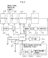
- FIG. 2 is a block diagram of the single lens reflex electronic still camera according to the first preferred embodiment.
- a half press signal and a full press signal are respectively inputted to a CPU 21 from a half press switch 22 and a full press switch 23, both of which are actuated by the operation of a shutter release button not shown in the figures.
- an actuation signal from a resize switch 40 for converting the data size of the image data is inputted to the CPU 21.
- the CPU 21 controls the operation of a CCD 26 of the imaging device 73 via a timing generator 24 and a driver 25.
- the operational timings of an analog signal processing circuit 27 and of an A/D conversion circuit 28 are controlled by the output signal of the timing generator 24.
- the CPU 21 controls the driving of a white balance detection processing circuit 35.
- a color filter is provided upon the pixel region of the CCD 26.
- the full press switch 23 When subsequently to the actuation to ON of the half press switch 22 the full press switch 23 is actuated to ON, the quick return mirror 71 is rotated to its upper position.
- the light from the photographic subject which passes through the interchangeable lens 90 is focused thereby into an image upon the light reception surface of the CCD 26, and signal electric charges are accumulated in the CCD 26 according to the brightness of the image of the photographic subject.
- These signal electric charges accumulated in the CCD 26 are emitted by the driver 25 and are inputted to the analog signal processing unit 27 which comprises an AGC circuit and a CDS circuit.
- This analog signal processing circuit 27 performs analog processing such as gain control, noise removal and the like upon the analog image signal which has been inputted.
- the image signal after this analog processing is converted into a digital signal by the A/D conversion circuit 28.
- the image data which has been thus converted into digital format is fed to an image processing circuit 29 which may for example be an ASIC, which performs image pre-processing such as white balance adjustment, contour compensation, gamma correction, and the like.
- the white balance detection processing circuit 35 comprises a white balance sensor 35A (the white balance sensor 86 of FIG. 1) which is a color temperature sensor, an A/D conversion circuit 35B which converts the analog signal from the white balance sensor 35A into a digital signal, and a CPU 35C which generates a white balance adjustment signal based upon this digital color temperature signal.
- the white balance sensor 35A may, for example, comprise a plurality of photoelectric conversion elements for red light, blue light and green light each of which has its own characteristic sensitivity, and said white balance sensor 35A receives light from the image of the photographic field as a whole.
- the CPU 35C calculates a R-gain and a B-gain based upon the output of a plurality of photoelectric conversion elements.
- the white balance sensor 86 of FIG. 1 may be constituted by a two dimensional CCD of 24 columns X 20 rows.
- the CCD is divided into 16 regions, and in each of the regions there is arranged a plurality of elements, each of which has its own sensitivity to red light, blue light or green light.
- the digital image data which has thus been pre-processed is further subjected to image data size conversion processing.
- the image data after resize processing is then subjected to format processing (image post-processing) for JPEG compression, and then is temporarily stored in a buffer memory 30.
- This image data which has been stored in the buffer memory 30 is processing into image data for display by a display image generation circuit 31, and is then displayed upon an external monitor 32 such as a LCD or the like as the result of photography. Furthermore, this image data which has been stored in the buffer memory 30 is also subjected to data compression at a predetermined compression ratio by the JPEG method, and is then stored upon a recording medium 34 such as a compact flash memory card (CF card) or the like.
- CF card compact flash memory card
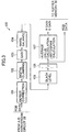
- FIGS. 3 and 4 are block diagrams showing the details of the image processing circuit 29.
- FIG. 3 shows a line processing circuit 100 which performs line by line signal processing upon the image data from the CCD 26.
- the 12 bit R, G, and B signals which are outputted from the A/D conversion circuit 28 are subjected to the abovementioned image pre-processing.
- FIG. 4 shows a block processing circuit 200 which performs signal processing upon the image data which have been processed by the line processing circuit 100 for each n x m pixels data at a time, in other words one block at a time.
- Image post-processing may be performed upon the image data in the manner described above for each 20 x 20 pixel region, for each 16 x 16 pixel region, for each 12 x 12 pixel region, or for each 8 x 8 pixel region, as appropriate. It should be understood that, in this specification, the image processing circuit 29 will be explained in terms of a hardware implementation thereof for the convenience of description, although in actual fact it could be implemented in software by utilizing a plurality of processors.
- the line processing circuit 100 is shown as being comprised of a defect correction circuit 101, a digital clamp circuit 102, a gain circuit 103, a white balance circuit 104, a black level circuit 105, a gamma correction circuit 106, and an average value and histogram calculation circuit 107.
- the defect correction circuit 101 corrects the data in the output of the CCD 26, each line at a time in point order (point by point), for any pixels which has any defect (which are specified in advance, and whose addresses are set into registers of the CPU 21). For each line at a time in point order, the digital clamp circuit 102 subtracts from the signal for each pixel of this line outputted by the CCD 26 the weighted average of the signals from a plurality of pixels, which are thus used as so-called optical black.
- the gain circuit 103 impartially multiplies each of the R, G, and B signals which are outputted from the CCD 26 by a predetermined gain, and also performs deviation correction of the sensitivity of the CCD 26 for the G signal. Moreover, the gain circuit 103 also performs deviation correction of sensitivity ratio of the CCD 26 for the R and B signals.
- the white balance circuit 104 For each line at a time in the output of the CCD 26 in point order, the white balance circuit 104 multiplies the R and B signals by the white balance adjustment coefficients which are determined in advance as described above and are stored in advance in the registers of the CPU 21, in other words by the R gain and the B gain. Based upon the image data which have been corrected by this white balance circuit 104, the white balance is further subjected to fine adjustment by a white balance fine adjustment circuit which will be described hereinafter. For each line at a time in the output of the CCD 26 in point order, the black level circuit 105 adds to each of the R, G, and B signals a value which is determined in advance and is stored in a register of the CPU 21.
- the gamma correction circuit 106 performs gamma correction using a gradation look up table for each line at a time in the output of the CCD 26 in point order. It should be understood that the 12 bit R, G, and B signals are converted by this gamma correction into 8 bit RGB data.
- the average value and histogram calculation circuit 107 extracts from within the image data after gamma correction the image data for a 512 x 512 region which is specified, for example, by taking the central portion of the focus detection region as a center, and calculates a RF-gain for white balance fine adjustment for the R signal and a BF-gain for white balance fine adjustment for the B signal using the following Equations (1) and (2). These calculated values for the RF-gain and the BF-gain are stored in registers of the CPU 21.
- FIG. 5 is a figure showing a color separation filter which is arranged over the pixel region of the CCD 26 and which utilizes the Bayer arrangement. For example, if an arrangement of color filters like that shown in FIG.
- the average values of the R, G, and B signals are calculated by using the Equations (3) through (5), and, as shown in Equations (1) and (2), the RF-gain and the BF-gain for white balance fine adjustment are calculated from the ratio of the average value G-ave of the G signal to the average value R-ave of the R signal, and the ratio of the average value G-ave of the G signal to the average value B-ave of the B signal, respectively.
- the block processing circuit 200 is comprised of a white balance fine adjustment circuit 210, an image data size conversion processing circuit 240, a changeover circuit 250, and an interpolation/contour processing circuit 220.
- the white balance fine adjustment circuit 210 performs fine adjustment of the white balance, with respect to the R signal and the B signal which are stored in the buffer memory 30 after the above described processing up to the gamma correction circuit 106, by multiplying each of the R and B signals in the specified pixel region by, respectively, the RF-gain and the BF-gain which are used for white balance fine adjustment and which have been calculated by the average value circuit 107.
- the image data size conversion processing circuit 240 converts the amount of data, in other words the data size, which has been generated for one photographic frame of image data without performing any subsampling process.
- the image data after data size conversion is outputted as image data for each 20 x 20 pixel region.
- the present invention is distinguished in particular by the fact that data size conversion is performed without discarding the order of the color components which corresponds to the arrangement of the color components of the color separation filter which is disposed over the pixel region of the CCD 26, and moreover without lowering the spatial frequency of the image data.
- conversion of the data size it goes without saying that information relating to the contours of the photographic subject and so on is preserved.
- the example will be employed of performing size conversion for a single frame by an area ratio of 9/16, in other words when resizing the data size in both the vertical direction and the horizontal direction by a ratio of 3/4.
- the term of resizing means that a new image data which has pixels a number of which is different from and values of which are different from the image data before resizing is generated and that a new pixel plane which has a spatial frequency different from one in the image data before resizing is generated.
- the resizing process calculates the data for one pixel by linear interpolation by using data of the same color signals which correspond to two adjacent pixels which position every two pixels.
- the data for three pixels is calculated per the data for each four pixels.
- the term of calculating by liner interpolation means, as mentioned hereinafter, that weighted coefficients are obtained by taking the relative positional relationship between pixels before resizing and new pixels generated by resizing into account and a weighted addition is performed with the weighted coefficients.
- the first RGRG.... line shown in FIG. 5 will be considered.
- the target pixel n be the one in the first row and the first column which provides a R signal.
- the values of the R component and the G component after the resizing procedure are calculated according to the following Equations (6) through (11):
- R(1,1) ⁇ n+(n+2) ⁇ /2
- G(1,2) ⁇ (n+1)+(n+3) ⁇ /2
- R(1,3) ⁇ 5(n+2)+27(n+4) ⁇ /32
- G(1,4) ⁇ 5(n+3)+27(n+5) ⁇ /32
- R(1,5) ⁇ 27(n+6)+5(n+8) ⁇ /32
- G(1,6) ⁇ 27(n+7)+5(n+9) ⁇ /32
- the three R components R(1,1), R(1,3), and R(1,5) in the group of target pixels from n to (n+8) are calculated at almost equal intervals in the horizontal direction.
- the three G components G(1,2), G(1,4), and G(1,6) in the group of target pixels from (n+1) to (n+9) are calculated at almost equal intervals in the horizontal direction.
- the next data are calculated by taking the target pixel (n+8) as the new target pixel. Accordingly the 3/4 resizing procedure calculates three data elements from four, since among the groups described above of 5 R signals and G signals the end one overlaps the first one of the next group.
- Equations (12) through (17) for the G component, the three G components G(2,1), G(2,3), and G(2,5) in the group of target pixels from n to (n+8), in other words in a range over which 5 G signals are obtained, are calculated at almost equal intervals in the horizontal direction. Furthermore, for the B component, the three B components B(2,2), B(2,4), and B(2,6) in the group of target pixels from (n+1) to (n+9), in other words in a range over which 5 B signals are obtained, are calculated at almost equal intervals in the horizontal direction.
- the next data are calculated by taking the target pixel (n+8) as the new target pixel n.
- the 3/4 resizing procedure calculates three data elements from four, since among the groups described above of 5 G signals and B signals the end one overlaps the first one of the next group.
- the RGRG.... line and the GBGB.... line before size conversion respectively become a RGRG.... line and a GBGB.... line after size conversion, and thus the order of arrangement of the color components in each line before and after the resizing procedure is the same.
- the three R components R(1,1), R(3,1), and R(5,1) in the group of target pixels from m to (m+8), in other words in a range over which 5 R signals are obtained, are calculated at almost equal intervals in the vertical direction.
- the three G components G(2,1), G(4,1), and G(6,1) in the group of target pixels from (m+1) to (m+9), in other words in a range over which 5 G signals are obtained are calculated at almost equal intervals in the vertical direction.
- the next data are calculated by taking the target pixel (m+8) as the new target pixel. Accordingly the 3/4 resizing procedure calculates three data elements from four, since among the groups described above of 5 R signals and G signals the end one overlaps the first one of the next group.
- Equations (24) through (29) for the G component, the three G components G(1,2), G(3,2), and G(5,2) in the group of target pixels from m to (m+8), in other words in a range over which 5 G signals are obtained, are calculated at almost equal intervals in the vertical direction. Furthermore, for the B component, the three B components B(2,2), B(4,2), and B(6,2) in the group of target pixels from (m+1) to (m+9), in other words in a range over which 5 B signals are obtained, are calculated at almost equal intervals in the vertical direction.
- the next data are calculated by taking the target pixel (m+8) as the new target pixel m.
- the 3/4 resizing procedure calculates three data elements from four, since among the groups described above of 5 G signals and B signals the end one overlaps the first one of the next group.
- the RGRG.... line and the GBGB.... line before size conversion respectively become a RGRG.... line and a GBGB.... line after size conversion, and thus the order of arrangement of the color components in each line before and after the resizing procedure is the same.
- the changeover circuit 250 upon commands from the CPU 21 (see FIG. 2), outputs to the interpolation/contour processing circuit 220 either the image data for the 20 x 20 pixel region which is output in order from the white balance fine adjustment circuit 210, or the image data for the 20 x 20 pixel region which is output in order from the image data size conversion processing circuit 240.
- the interpolation/contour processing circuit 220 performs formatting procedures for data compression according to the JPEG method for the block data of each 20 x 20 pixel region in order, for the image data after white balance fine adjustment, or after image data size conversion. As results of this formatting procedure a Y signal of a 16 x 8 pixel region, a Cb signal of an 8 x 8 pixel region, and a Cr signal of an 8 x 8 pixel region are generated.
- the luminance signal Y includes a luminance signal Y1 for the low frequency component of the G signal and a contour signal Y2 for its high frequency component, as will be described hereinafter.
- This interpolation/contour processing circuit 220 is comprised of a G interpolation circuit 221, a band pass filter (BPF) 222, a clip circuit 223, a gain circuit 224, a low pass filter (LPF) 225, a color difference signal generation circuit 226, an interpolation/low pass filter (LPF) circuit 228, a matrix circuit 229, an adder 230, and a median circuit 232.
- G interpolation circuit 221 a band pass filter (BPF) 222, a clip circuit 223, a gain circuit 224, a low pass filter (LPF) 225, a color difference signal generation circuit 226, an interpolation/low pass filter (LPF) circuit 228, a matrix circuit 229, an adder 230, and a median circuit 232.
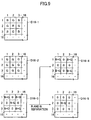
- the G interpolation circuit 221 calculates by interpolation the G component for the pixel regions of the R signal or the B signal for the data in the 16 x 16 pixel region around the center of each block signal for each 20 x 20 pixel region of the image data which is inputted from the white balance fine adjustment circuit 210, or from the image data size conversion processing circuit 240. In other words, as shown in FIG.
- the G interpolation circuit 221 calculates the G component of the vacancy (which is the pixel in the third row and the third column, and provides a B signal) in the middle of the 5 x 5 pixel data region D51 (from row 1 column 1 to row 5 column 5), and substitutes this value as the G component of the pixel in the third row and the third column of the output data set D16 (in which the "B" is surrounded by a circle) of the 16 x 16 pixel region.
- the G component of the vacancy (which is the pixel in the fourth row and the fourth column, and provides a R signal) in the center of the 5 x 5 pixel data region D52 (from the second row second column to the sixth row sixth column) is calculated, and this value is substituted as the G component of the pixel in the fourth row and the fourth column of the output data set D16 (in which the "R" is surrounded by a circle) of the 16 x 16 pixel region.
- the G interpolation procedure is performed for all the vacancies of the 16 x 16 pixel region, and thus the output data set D16 is obtained.
- the output data set D12 from this 12 x 12 pixel region is outputted respectively to the band pass filter 222 and the low pass filter 225, while on the other hand the output data set D16 from the 16 x 16 pixel region is outputted to the color difference signal generation circuit 226.
- the band pass filter 222 extracts the medium frequency component from the G signal of the 12 x 12 pixel region which is outputted from the G interpolation circuit 221 (however, this is the frequency component which is high enough to be able to extract the contour of the photographic subject, and it may for convenience be termed the high frequency component) .
- the BPF output data is obtained by multiplying the 5 x 5 pixel region data D5 (from row 5 column 5 to row 9 column 9) by the band pass filter coefficient, and this value is substituted as the data item (the bold "G") in the seventh row and seventh column of the output data set D8 of the 8 x 8 pixel region.
- the clip circuit 223 clips and cuts each element in the 8 x 8 pixel data region D8 which is output from the band pass filter 222 to a set level.
- the gain circuit 224 multiplies the output of the clip circuit 223 by a gain which is set in advance.
- the low pass filter 225 extracts the low frequency component in the G signal of the 12 x 12 pixel region which is outputted from the G interpolation circuit 221.
- the 5 x 5 pixel data region D5 (from the fifth row and fifth column to the ninth row and ninth column) is multiplied by the low pass filter coefficient and the LPF output data is obtained, and this value is substituted as the data (the hatched region) for the seventh row and seventh column of the 8 x 8 pixel region output data set D8.
- all of the pixel data for the 8 x 8 pixel region is substituted with the G data after LPF, and thus the output data set D8 is generated.
- the color difference signal generation circuit 226, as shown in FIG. 9, generates intermediate data D16-3 which include a (B-G) signal and a (R-G) signal, based upon the RGB signal input data D16-1 for the 16 x 16 pixel region and the G signal input data D16-2 for the 16 x 16 pixel region which has been outputted from the G interpolation circuit 221, among the image data which has been inputted from the white balance fine adjustment circuit 210 or the image data size conversion processing circuit 240. Furthermore, the intermediate data D16-3 is separated into output data D16-4 of a (B-G) color difference signal and output data D16-5 of a (R-G) color difference signal.
- the interpolation/LPF circuit 228 inputs the 8 bit (B-G) signal and (R-G) signal of the 16 x 16 pixel region which are outputted from the color difference signal generation circuit 226, performs interpolation calculation for this (B-G) signal and (R-G) signal one 5 x 5 pixel region at a time, and also simultaneously performs a low pass filtering procedure in which it extracts the low band signal therefrom, so that as a result it outputs a (B-G) signal and a (R-G) signal of a 12 x 12 pixel region to the Cb and Cr matrix sections of the matrix circuit 229 respectively. Furthermore, a (B-G) signal and a (R-G) signal of a 8 x 8 pixel region are outputted to a Y matrix section of the matrix circuit 229.
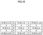
- i is an integer greater than or equal to zero and less than or equal to (2n+1), while k is an integer greater than or equal to zero and less than n.
- N is equal to 2 since the sampling points are interpolated at a period of two pixels as shown in FIGS. 5 and 10, and the sums of the odd numbered filter coefficients and the sums of the even numbered filter coefficients must be equal.
- ⁇ C(2*i) ⁇ C(2*i+1)
- the case will be explained of performing interpolation/LPF processing upon the (R-G) signal while referring to FIG. 11.
- the data set D5 for the 5 x 5 pixel region (from the third row third column to the seventh row seventh column) is multiplied by the interpolation/LPF filter coefficient, and the (R-G) data for its central region (the fifth row and the fifth column) are calculated, and this is substituted as the fifth row fifth column data element in the output data set D12 for the 12 x 12 pixel region.
- the matrix circuit 229 comprises a Y matrix section, a Cb matrix section, and a Cr matrix section.
- the Y matrix section inputs the (B-G) signal and the (R-G) signal of the 8 x 8 pixel region from the interpolation/LPF circuit 228, and also inputs the G signal of the 8 x 8 pixel region from the low pass filter 225, and generates a luminance signal Y1 for the low frequency component of the 8 x 8 pixel region according to the following Equation (31).
- Y1(i,j) [Mkg ⁇ G(i,j)+Mkr1 ⁇ R-G(i,j)+Mkb1 ⁇ B-G(i,j)] where Mkg, Mkr1, and Mkb1 are matrix coefficients.
- the Cb matrix section and the Cr matrix section respectively input the (B-G) signal and the (R-G) signal of the 12 x 12 pixel region from the interpolation/LPF circuit 228, and respectively generate a Cb signal and a Cr signal of the 12 x 12 pixel region according to the following Equations (32) and (33).
- the adder 230 adds together the luminance signal Y1 of the low frequency component of the 8 x 8 pixel region which is outputted from the matrix circuit 229, and the contour extraction signal Y2 of the high frequency component of the 8 x 8 pixel region which is outputted from the gain circuit 224.
- This contour extraction signal Y2 which is outputted from the gain circuit 224 consists of the high frequency component extracted from the G signal of the 16 x 16 pixel region which has been G interpolated, in other words of an extracted contour.
- a luminance/contour extraction signal Y (Y1+Y2) for the image as a whole is calculated by adding together in the adder 230 the luminance signal Y1 which is calculated according to the above Equation (31) and the contour extraction signal Y2 which is calculated by the gain circuit 224. The result of this addition is stored in the buffer memory 30.
- the median circuit 233 inputs the Cb signal and the Cr signal of the 12 x 12 pixel region which are outputted from the matrix circuit 229, performs median processing by utilizing the nine points of 3 x 3 pixels which are included in the 5 x 5 pixel region, and outputs the Cb signal and the Cr signal of the 8 x 8 pixels.
- the median filtering procedure is performed upon the nine data elements D3-5 (marked with "X") of 3 x 3 pixels (from the fifth row fifth column to the ninth row ninth column) which are included in a 5 x 5 pixel region.
- these nine elements of data are sorted into ascending or descending order, and the median value thereof is taken as the data value after median processing.
- the data item after median processing which is obtained is substituted as the output data item D8 in the seventh row seventh column of the 8 x 8 pixels.
- the output data D8 of the 8 x 8 pixels is obtained for the Cb signal and the Cr signal.
- the output data consisting of the Cr signal and the Cb signal, is stored in the buffer memory 30.
- the JPEG compression circuit 33 For each of the input data elements in the 20 x 20 pixel region which has been inputted to the block processing circuit 200 as described above, based upon the Y signal of the 16 x 8 pixels which is generated by the adder circuit 230 and upon the Cr signal and the Cb signal of the 8 x 8 pixels which are generated by the median circuit 232, the JPEG compression circuit 33 extracts as one unit the Y, Cr, and Cb signals which have been formatted to an 8 x 8 pixel by the JPEG compression method, and thus compresses the entire image by repeating a per se known compression method. The compressed image data are stored upon the recording medium 34 via the CPU 21.
- each of the pixels of the CCD 26 accumulates electric charge, and after this accumulation has been completed the accumulated electric charge for all said pixels is read out (discharged) in order.
- the read out image signal has been processed by the analog signal processing circuit 27, it is converted into digital image data by the A/D conversion circuit 28.
- this image data is inputted into the image processing circuit 29, and the image processing described above is performed.
- This image processing circuit 29 performs procedures such as white balance adjustment, gamma gradation correction, image data size conversion processing, JPEG formatting processing, etc..
- the flow of control proceeds to the next step S24, in which the image data after image processing is temporarily stored in the buffer memory 30.
- the image data is read out from the buffer memory 30, and this data is compressed by the JPEG compression circuit 33.
- the image data after compression is stored upon the recording medium 34, and then the procedure shown in FIG. 13 terminates.
- the data for one pixel is calculated by linear interpolation by using the data of the same color signals of the adjacent two pixels which have another pixel between them. It would also be possible to perform an interpolation procedure based upon a Sinc function by using the data of the same color signals of the adjacent five or six pixels each of which sits every two pixels.
- an interpolation procedure based upon a Sinc function by using the data of the same color signals of the adjacent five or six pixels each of which sits every two pixels.
- the RGRG.... line and the GBGB.... line before size conversion respectively also become the RGRG.... line and the GBGB.... line after size conversion as well, and the order of arrangement of the color components before and after the resizing procedure is the same.
- the group from the target pixel n to (n+4) in other words the three R components R(1,1), R(1,3), and R(1,5) are calculated at almost equal intervals in the horizontal direction in the range which is held by three R signals.
- the group from the target pixel (n+1) to (n+5) in other words the three G components G(1,2), G(1,4), and G(1,6) are calculated at almost equal intervals in the horizontal direction in the range which is held by three G signals.
- the next data set is calculated by setting the target pixel (n+4) as the new target pixel n. If the calculations for the GBGB.... lines in the vertical direction are performed in the same manner, it is possible to convert the data which constitute a single photographic image by 3/2 in both the horizontal direction and the vertical direction, in other words to convert the size of the entire data set by 9/4. It should be understood that, although for the convenience of explanation the calculation procedures for the horizontal direction and for the vertical direction have been explained as being done separately, in actual fact, the calculation procedures in both these directions may be performed together as a matrix calculation. The results are the same when performing these calculations for the two directions together, as if they were to be performed separately and independently.
- the image data size conversion processing circuit 240 calculates the data for one pixel by linear interpolation using the data of the same color signals of the adjacent two pixels which have another pixel between them. Furthermore, any desired magnification ratio may be employed. Yet further, there is no deterioration of the image quality after resizing, since the generation of color artifact and reduction of the spatial frequency are suppressed by the calculation by linear interpolation.
- the data for one pixel is calculated by linear interpolation by using the data of the same color signals of the adjacent two pixels each of which is from every two pixels. It would also be possible to perform an interpolation procedure based upon a Sinc function by using the data of the same color signals of the adjacent four pixels each of which sits every two pixels.
- an interpolation procedure based upon a Sinc function by using the data of the same color signals of the adjacent four pixels each of which sits every two pixels.
- the next data set is calculated by setting the target pixel (n+4) as the new target pixel n.
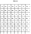
- FIG. 14 is a figure for explanation of a color separation filter in which G colored, Ye colored, Cy colored, and Ma colored complementary color filters are arranged in correspondence with the pixels of the CCD 26. It is also possible to perform resizing procedures by the various methods described above in this case in which the filters for the same color component are arranged every two pixels in both the horizontal direction and in the vertical direction in this manner.
- the present invention may also be utilized for image data of a single color in which the entire data that constitutes a single photographic image is constituted by the G component for example.
- the resizing procedure of the present invention can be set at will to any resizing ratio, and in this aspect it differs from the simple prior art subsampling procedure. Accordingly, the resizing ratio may be set to any desired value, and is not to be considered as being limited to the values described above.
- the image data size conversion processing circuit 240 in the form of software as an image data size conversion processing program upon a recording medium such as a CD-ROM or a floppy disk or the like.
- the image data which has been imaged by the CCD and has been converted to digital form is stored upon a recording medium for image data of high capacity, and, after this recording medium has been set into a personal computer and the image data has been read thereinto, a resizing procedure like the one described above is performed by the above described image data size conversion processing program.
- FIG. 3 it is possible to store the raw original R, G, and B output data from the gamma correction circuit 106 upon the recording medium 34, to set this recording medium 34 into a personal computer, and to perform the resizing procedure upon the raw data.
- FIG. 16 illustrates how this may be achieved.
- a personal computer 300 performs the image data size conversion processing explained above.
- the personal computer 300 has a function of connecting with a telecommunication line 301.
- a computer 302 is a server computer which provides the image data size conversion processing program and stores the image data size conversion processing program in a recording medium such as a hard disk 303.
- the telecommunication line 301 may be a telecommunication line for connection with the Internet, for personal computer communication or the like or it may be a dedicated telecommunication line.
- the computer 302 reads out the image data size conversion processing program stored in the hard disk 303, and transmits the image data size conversion processing program to the personal computer 300 via the telecommunication line 301.
- the image data size conversion processing program is embodied in a carrier wave as a data signal and is transmitted via the telecommunication line 301.
- a CD-ROM 304 or the like is employed.
- the image data size conversion processing program is provided as various kinds of computer-readable computer program product, such as a recording medium, a carrier wave and the like.
- the present invention has been explained in terms of its application to a single lens reflex electronic still camera, it should be understood that the present invention can also be applied to the case of an electronic still camera which is not equipped with an interchangeable lens, or to a digital video camera which takes a moving image.
- the circuit structure has been shown, for example, the following modification thereof is also possible.
- the explanation has been made in terms of performing image processing in single units of any one of 20 x 20, 16 x 16, 12 x 12, and 8 x 8 blocks.
- the explanation has been made in terms of the image data size conversion processing circuit 240 outputting image data after resizing in units of a 20 x 20 pixel region.
- the block size for such processing is not to be considered as being limited to the above cited example values; it would also be acceptable, for example, to perform the image processing in units of one 5 x 5 pixel region.
- the image data size conversion processing circuit 240 performed the resizing processing upon the image data after white balance fine adjustment. As described above, it is possible to reduce the resize processing time and the memory capacity which is required for the resizing procedure by performing the resizing procedure before performing the pixel interpolation procedure. Accordingly, provided that the resizing procedure is performed upon the image data before the pixel interpolation procedure, it does not necessarily need to be performed after the white balance fine adjustment, and it may be performed, for example, upon the image data after it has been digitally clamped by the line processing circuit of FIG. 3.
- the R component, the G component, and the B component corresponds to the plurality of color components
- the color separation filter corresponds to the color separation means
- the CCD 26 corresponds to the imaging means
- the A/D conversion circuit 28 corresponds to the A/D conversion means
- the image data size conversion processing circuit 240 corresponds to the data size conversion means
- the interpolation/contour processing circuit 220 corresponds to the image processing means.
Applications Claiming Priority (2)
| Application Number | Priority Date | Filing Date | Title |
|---|---|---|---|
| JP2000270396 | 2000-09-06 | ||
| JP2000270396A JP5108172B2 (ja) | 2000-09-06 | 2000-09-06 | 画像データサイズ変換処理装置、電子スチルカメラ、および画像データサイズ変換処理用記録媒体 |
Publications (3)
| Publication Number | Publication Date |
|---|---|
| EP1187455A2 true EP1187455A2 (de) | 2002-03-13 |
| EP1187455A3 EP1187455A3 (de) | 2003-05-21 |
| EP1187455B1 EP1187455B1 (de) | 2014-08-06 |
Family
ID=18756843
Family Applications (1)
| Application Number | Title | Priority Date | Filing Date |
|---|---|---|---|
| EP01307532.0A Expired - Lifetime EP1187455B1 (de) | 2000-09-06 | 2001-09-05 | Bilddatenverarbeitungsvorrichtung und elektronische Kamera |
Country Status (3)
| Country | Link |
|---|---|
| US (4) | US20020044778A1 (de) |
| EP (1) | EP1187455B1 (de) |
| JP (1) | JP5108172B2 (de) |
Cited By (5)
| Publication number | Priority date | Publication date | Assignee | Title |
|---|---|---|---|---|
| WO2003085963A1 (en) * | 2002-04-02 | 2003-10-16 | Freescale Semiconductor, Inc. | Digital color image pre-processing |
| US7373020B2 (en) | 2003-06-05 | 2008-05-13 | Olympus Corporation | Image processing apparatus and image processing program |
| CN101312532B (zh) * | 2007-05-24 | 2010-12-22 | 索尼株式会社 | 摄像装置、摄像电路以及摄像方法 |
| US8320714B2 (en) | 2007-06-13 | 2012-11-27 | Olympus Corporation | Image processing apparatus, computer-readable recording medium for recording image processing program, and image processing method |
| CN111988546A (zh) * | 2020-09-15 | 2020-11-24 | 哈尔滨工程大学 | 一种倍增ccd倍增增益及读出噪声测量方法 |
Families Citing this family (53)
| Publication number | Priority date | Publication date | Assignee | Title |
|---|---|---|---|---|
| JP4658401B2 (ja) * | 2001-07-27 | 2011-03-23 | オリンパス株式会社 | 撮像装置 |
| DE60130671D1 (de) * | 2001-12-24 | 2007-11-08 | St Microelectronics Srl | Verfahren zur Kontrastverbesserung in digitalen Farbbildern |
| FR2840093B1 (fr) * | 2002-05-27 | 2006-02-10 | Real Eyes 3D | Procede de numerisation par camera avec correction de la deformation et amelioration de la resolution |
| JP3934506B2 (ja) * | 2002-08-06 | 2007-06-20 | オリンパス株式会社 | 撮像システムおよび画像処理プログラム |
| JP2004147092A (ja) | 2002-10-24 | 2004-05-20 | Canon Inc | 信号処理装置、撮像装置、及び制御方法 |
| KR20040047383A (ko) * | 2002-11-29 | 2004-06-05 | 장영조 | Cmos 이미지센서와 칼라 보간 알고리즘을 이용한 영상처리방법 및 장치. |
| KR20040052150A (ko) * | 2002-12-13 | 2004-06-19 | 장영조 | Cmos 이미지센서와 칼라 보간 및 화이트 밸런스알고리즘을 이용한 영상처리 방법 및 장치. |
| JP4497945B2 (ja) * | 2003-02-04 | 2010-07-07 | キヤノン株式会社 | 撮像装置 |
| US8471852B1 (en) | 2003-05-30 | 2013-06-25 | Nvidia Corporation | Method and system for tessellation of subdivision surfaces |
| JP3942569B2 (ja) * | 2003-09-04 | 2007-07-11 | オリンパス株式会社 | 撮像装置および画像データの変換方法 |
| JP2005167974A (ja) * | 2003-11-10 | 2005-06-23 | Seiko Epson Corp | 画像処理方法及び画像処理装置、画像処理プログラム並びに半導体装置 |
| US7656561B2 (en) | 2004-05-31 | 2010-02-02 | Phase One A/S | Image compression for rapid high-quality imaging |
| US8571346B2 (en) * | 2005-10-26 | 2013-10-29 | Nvidia Corporation | Methods and devices for defective pixel detection |
| US7885458B1 (en) | 2005-10-27 | 2011-02-08 | Nvidia Corporation | Illuminant estimation using gamut mapping and scene classification |
| US7750956B2 (en) * | 2005-11-09 | 2010-07-06 | Nvidia Corporation | Using a graphics processing unit to correct video and audio data |
| US8588542B1 (en) | 2005-12-13 | 2013-11-19 | Nvidia Corporation | Configurable and compact pixel processing apparatus |
| JP4769567B2 (ja) * | 2005-12-16 | 2011-09-07 | キヤノン株式会社 | 撮像装置、撮像装置の制御方法、コンピュータプログラム及び記憶媒体 |
| US8737832B1 (en) | 2006-02-10 | 2014-05-27 | Nvidia Corporation | Flicker band automated detection system and method |
| CN101047862B (zh) * | 2006-03-30 | 2010-12-08 | 联阳半导体股份有限公司 | 用于贝尔滤光片数组影像的彩色补插值法 |
| EP1884893A1 (de) * | 2006-08-03 | 2008-02-06 | Mitsubishi Electric Information Technology Centre Europe B.V. | Bildbeschreibung durch dünnbesetztes Integral mit Anwendung in der Bewegungsanalyse |
| US8594441B1 (en) | 2006-09-12 | 2013-11-26 | Nvidia Corporation | Compressing image-based data using luminance |
| US8723969B2 (en) * | 2007-03-20 | 2014-05-13 | Nvidia Corporation | Compensating for undesirable camera shakes during video capture |
| US8564687B2 (en) * | 2007-05-07 | 2013-10-22 | Nvidia Corporation | Efficient determination of an illuminant of a scene |
| US8698917B2 (en) * | 2007-06-04 | 2014-04-15 | Nvidia Corporation | Reducing computational complexity in determining an illuminant of a scene |
| WO2008150017A1 (ja) * | 2007-06-07 | 2008-12-11 | Sony Corporation | 信号処理方法および信号処理装置 |
| JP5191168B2 (ja) * | 2007-06-11 | 2013-04-24 | 株式会社ニコン | 焦点検出装置および撮像装置 |
| US8724895B2 (en) * | 2007-07-23 | 2014-05-13 | Nvidia Corporation | Techniques for reducing color artifacts in digital images |
| US8570634B2 (en) * | 2007-10-11 | 2013-10-29 | Nvidia Corporation | Image processing of an incoming light field using a spatial light modulator |
| US9177368B2 (en) * | 2007-12-17 | 2015-11-03 | Nvidia Corporation | Image distortion correction |
| US8780128B2 (en) * | 2007-12-17 | 2014-07-15 | Nvidia Corporation | Contiguously packed data |
| JP5242180B2 (ja) * | 2008-01-23 | 2013-07-24 | オリンパス株式会社 | 画像処理装置、画像信号補正方法、補正マトリクス算出方法及び撮像装置 |
| US8698908B2 (en) * | 2008-02-11 | 2014-04-15 | Nvidia Corporation | Efficient method for reducing noise and blur in a composite still image from a rolling shutter camera |
| US9379156B2 (en) * | 2008-04-10 | 2016-06-28 | Nvidia Corporation | Per-channel image intensity correction |
| WO2010016166A1 (ja) * | 2008-08-04 | 2010-02-11 | パナソニック株式会社 | 撮像装置、画像処理方法、画像処理プログラム及び半導体集積回路 |
| US8373718B2 (en) * | 2008-12-10 | 2013-02-12 | Nvidia Corporation | Method and system for color enhancement with color volume adjustment and variable shift along luminance axis |
| JP5191407B2 (ja) * | 2009-01-20 | 2013-05-08 | 三洋電機株式会社 | 画像処理装置 |
| US8749662B2 (en) | 2009-04-16 | 2014-06-10 | Nvidia Corporation | System and method for lens shading image correction |
| JP5523802B2 (ja) * | 2009-11-25 | 2014-06-18 | 株式会社東芝 | 画像処理装置 |
| US8698918B2 (en) * | 2009-10-27 | 2014-04-15 | Nvidia Corporation | Automatic white balancing for photography |
| JP5719986B2 (ja) * | 2010-10-20 | 2015-05-20 | パナソニックIpマネジメント株式会社 | 画像処理装置および画像処理方法 |
| EP2645722A4 (de) * | 2011-03-11 | 2014-05-14 | Fujifilm Corp | Bildgebungsvorrichtung und verfahren zur steuerung von deren betrieb |
| WO2012164896A1 (ja) | 2011-05-31 | 2012-12-06 | パナソニック株式会社 | 画像処理装置及び画像処理方法並びにデジタルカメラ |
| JP5853166B2 (ja) | 2011-06-08 | 2016-02-09 | パナソニックIpマネジメント株式会社 | 画像処理装置及び画像処理方法並びにデジタルカメラ |
| US9798698B2 (en) | 2012-08-13 | 2017-10-24 | Nvidia Corporation | System and method for multi-color dilu preconditioner |
| US9508318B2 (en) | 2012-09-13 | 2016-11-29 | Nvidia Corporation | Dynamic color profile management for electronic devices |
| US9307213B2 (en) | 2012-11-05 | 2016-04-05 | Nvidia Corporation | Robust selection and weighting for gray patch automatic white balancing |
| US9756222B2 (en) | 2013-06-26 | 2017-09-05 | Nvidia Corporation | Method and system for performing white balancing operations on captured images |
| US9826208B2 (en) | 2013-06-26 | 2017-11-21 | Nvidia Corporation | Method and system for generating weights for use in white balancing an image |
| JP6557451B2 (ja) * | 2014-05-07 | 2019-08-07 | キヤノン株式会社 | 撮像装置およびその制御方法ならびにプログラム |
| CN105427776B (zh) * | 2016-01-26 | 2018-08-07 | 深圳市华星光电技术有限公司 | 液晶面板影像残留检测方法和装置 |
| US10863158B2 (en) * | 2016-05-17 | 2020-12-08 | Canon Kabushiki Kaisha | Image processing apparatus, image processing method, and program |
| WO2018051809A1 (ja) * | 2016-09-16 | 2018-03-22 | ソニーセミコンダクタソリューションズ株式会社 | 撮像装置、及び、電子機器 |
| CN115348432A (zh) * | 2022-08-15 | 2022-11-15 | 上海壁仞智能科技有限公司 | 数据处理方法及装置、图像处理方法、电子设备及介质 |
Citations (2)
| Publication number | Priority date | Publication date | Assignee | Title |
|---|---|---|---|---|
| US5418565A (en) | 1994-02-15 | 1995-05-23 | Eastman Kodak Company | CFA compatible resolution reduction in a single sensor electronic camera |
| WO2000019728A1 (en) | 1998-09-29 | 2000-04-06 | Intel Corporation | A new scaling algorithm for efficient color representation/recovery in video |
Family Cites Families (20)
| Publication number | Priority date | Publication date | Assignee | Title |
|---|---|---|---|---|
| US4821121A (en) * | 1983-04-08 | 1989-04-11 | Ampex Corporation | Electronic still store with high speed sorting and method of operation |
| US5253046A (en) * | 1991-03-07 | 1993-10-12 | Canon Kabushiki Kaisha | Color image pickup apparatus for object image conversion |
| KR950011530B1 (ko) * | 1992-09-25 | 1995-10-05 | 삼성전자주식회사 | 디지탈 주밍 시스템 |
| US5481304A (en) * | 1992-09-25 | 1996-01-02 | Samsung Electronics Co., Ltd. | Apparatus for zooming a digital video signal of a predetermined color order which is derived from a charge-coupled device |
| US5349451A (en) * | 1992-10-29 | 1994-09-20 | Linotype-Hell Ag | Method and apparatus for processing color values |
| JPH077634A (ja) | 1993-06-15 | 1995-01-10 | Toshiba Corp | デジタル信号処理装置 |
| US5493335A (en) * | 1993-06-30 | 1996-02-20 | Eastman Kodak Company | Single sensor color camera with user selectable image record size |
| JP3429061B2 (ja) | 1994-05-19 | 2003-07-22 | 富士写真フイルム株式会社 | 電子スチルカメラ |
| JPH08317295A (ja) * | 1995-05-16 | 1996-11-29 | Olympus Optical Co Ltd | デジタル画像記録装置およびデジタル画像再生装置 |
| WO1997030375A1 (en) * | 1996-02-13 | 1997-08-21 | Obsidian Imaging, Inc. | Method and apparatus for configuring a camera through external means |
| JP3503372B2 (ja) * | 1996-11-26 | 2004-03-02 | ミノルタ株式会社 | 画素補間装置及びその画素補間方法 |
| EP0935881A2 (de) * | 1997-07-15 | 1999-08-18 | Koninklijke Philips Electronics N.V. | Farbabtastwertinterpolation |
| JPH11103407A (ja) * | 1997-09-29 | 1999-04-13 | Nec Corp | Ccdデータ画素補間回路およびこのccdデータ画素 補間回路を備えたデジタルスチルカメラ |
| JP3410646B2 (ja) | 1997-10-14 | 2003-05-26 | シャープ株式会社 | 画質補正回路 |
| US6348929B1 (en) * | 1998-01-16 | 2002-02-19 | Intel Corporation | Scaling algorithm and architecture for integer scaling in video |
| US6650366B2 (en) * | 1998-03-26 | 2003-11-18 | Eastman Kodak Company | Digital photography system using direct input to output pixel mapping and resizing |
| US6937277B1 (en) * | 1998-04-24 | 2005-08-30 | Canon Kabushiki Kaisha | Image input apparatus employing read region size determination |
| JPH11308535A (ja) | 1998-04-24 | 1999-11-05 | Canon Inc | 撮像装置 |
| JP2000175205A (ja) * | 1998-12-01 | 2000-06-23 | Asahi Optical Co Ltd | 画像読取装置 |
| US6958772B1 (en) * | 1999-01-20 | 2005-10-25 | Canon Kabushiki Kaisha | Image sensing apparatus and image processing method therefor |
-
2000
- 2000-09-06 JP JP2000270396A patent/JP5108172B2/ja not_active Expired - Lifetime
-
2001
- 2001-09-05 US US09/945,847 patent/US20020044778A1/en not_active Abandoned
- 2001-09-05 EP EP01307532.0A patent/EP1187455B1/de not_active Expired - Lifetime
-
2005
- 2005-12-29 US US11/319,274 patent/US20060132628A1/en not_active Abandoned
-
2011
- 2011-04-18 US US13/064,811 patent/US20110216230A1/en not_active Abandoned
-
2013
- 2013-03-14 US US13/827,703 patent/US8896722B2/en not_active Expired - Fee Related
Patent Citations (2)
| Publication number | Priority date | Publication date | Assignee | Title |
|---|---|---|---|---|
| US5418565A (en) | 1994-02-15 | 1995-05-23 | Eastman Kodak Company | CFA compatible resolution reduction in a single sensor electronic camera |
| WO2000019728A1 (en) | 1998-09-29 | 2000-04-06 | Intel Corporation | A new scaling algorithm for efficient color representation/recovery in video |
Cited By (7)
| Publication number | Priority date | Publication date | Assignee | Title |
|---|---|---|---|---|
| WO2003085963A1 (en) * | 2002-04-02 | 2003-10-16 | Freescale Semiconductor, Inc. | Digital color image pre-processing |
| US7102669B2 (en) | 2002-04-02 | 2006-09-05 | Freescale Semiconductor, Inc. | Digital color image pre-processing |
| US7373020B2 (en) | 2003-06-05 | 2008-05-13 | Olympus Corporation | Image processing apparatus and image processing program |
| CN101312532B (zh) * | 2007-05-24 | 2010-12-22 | 索尼株式会社 | 摄像装置、摄像电路以及摄像方法 |
| US8320714B2 (en) | 2007-06-13 | 2012-11-27 | Olympus Corporation | Image processing apparatus, computer-readable recording medium for recording image processing program, and image processing method |
| CN111988546A (zh) * | 2020-09-15 | 2020-11-24 | 哈尔滨工程大学 | 一种倍增ccd倍增增益及读出噪声测量方法 |
| CN111988546B (zh) * | 2020-09-15 | 2023-03-31 | 哈尔滨工程大学 | 一种倍增ccd倍增增益及读出噪声测量方法 |
Also Published As
| Publication number | Publication date |
|---|---|
| US20110216230A1 (en) | 2011-09-08 |
| JP5108172B2 (ja) | 2012-12-26 |
| JP2002084547A (ja) | 2002-03-22 |
| US20060132628A1 (en) | 2006-06-22 |
| EP1187455B1 (de) | 2014-08-06 |
| EP1187455A3 (de) | 2003-05-21 |
| US8896722B2 (en) | 2014-11-25 |
| US20130194449A1 (en) | 2013-08-01 |
| US20020044778A1 (en) | 2002-04-18 |
Similar Documents
| Publication | Publication Date | Title |
|---|---|---|
| EP1187455B1 (de) | Bilddatenverarbeitungsvorrichtung und elektronische Kamera | |
| US7253836B1 (en) | Digital camera, storage medium for image signal processing, carrier wave and electronic camera | |
| US7227574B2 (en) | Image capturing apparatus | |
| US7973831B2 (en) | Solid-state image sensor and imaging apparatus using the same | |
| KR100481109B1 (ko) | 화상 신호 처리 장치 | |
| JPH04284087A (ja) | 電子スチルカメラ | |
| WO2008150017A1 (ja) | 信号処理方法および信号処理装置 | |
| JPH10248068A (ja) | 撮像装置及び画像処理装置 | |
| JP4272443B2 (ja) | 画像処理装置および画像処理方法 | |
| JP4182566B2 (ja) | デジタルカメラおよびコンピュータ読み取り可能な記録媒体 | |
| JP5291788B2 (ja) | 撮像装置 | |
| JP2002335454A (ja) | 画像処理装置、画像処理方法及び撮像装置 | |
| JP2003101815A (ja) | 信号処理装置及び信号処理方法 | |
| JP2007180893A (ja) | 画像処理装置および撮像装置 | |
| JP7022544B2 (ja) | 画像処理装置及び方法、及び撮像装置 | |
| JP4133179B2 (ja) | 画像信号処理装置 | |
| JP3733182B2 (ja) | 撮像装置および縦縞除去方法 | |
| JP4687750B2 (ja) | デジタルカメラおよび画像信号処理用記憶媒体 | |
| JP2002209100A (ja) | 画像処理装置および画像処理方法 | |
| JP3893489B2 (ja) | 信号処理装置および信号処理方法 | |
| JP2002209224A (ja) | 画像処理装置、画像処理方法および記録媒体 | |
| JP2006115147A (ja) | 撮像装置 | |
| JPH0614333A (ja) | デジタルビデオカメラ信号処理装置 | |
| JP2000023083A (ja) | デジタルカメラおよび画像信号処理用記憶媒体 | |
| JP2000023084A (ja) | デジタルカメラ及び画像信号処理用記憶媒体 |
Legal Events
| Date | Code | Title | Description |
|---|---|---|---|
| PUAI | Public reference made under article 153(3) epc to a published international application that has entered the european phase |
Free format text: ORIGINAL CODE: 0009012 |
|
| AK | Designated contracting states |
Kind code of ref document: A2 Designated state(s): AT BE CH CY DE DK ES FI FR GB GR IE IT LI LU MC NL PT SE TR |
|
| AX | Request for extension of the european patent |
Free format text: AL;LT;LV;MK;RO;SI |
|
| PUAL | Search report despatched |
Free format text: ORIGINAL CODE: 0009013 |
|
| AK | Designated contracting states |
Designated state(s): AT BE CH CY DE DK ES FI FR GB GR IE IT LI LU MC NL PT SE TR |
|
| AX | Request for extension of the european patent |
Extension state: AL LT LV MK RO SI |
|
| RIC1 | Information provided on ipc code assigned before grant |
Ipc: 7H 04N 1/393 A Ipc: 7H 04N 9/04 B Ipc: 7H 04N 1/56 B |
|
| 17P | Request for examination filed |
Effective date: 20031104 |
|
| AKX | Designation fees paid |
Designated state(s): AT BE CH CY DE DK ES FI FR GB GR IE IT LI LU MC NL PT SE TR |
|
| 17Q | First examination report despatched |
Effective date: 20071218 |
|
| RAP1 | Party data changed (applicant data changed or rights of an application transferred) |
Owner name: NIKON CORPORATION |
|
| GRAP | Despatch of communication of intention to grant a patent |
Free format text: ORIGINAL CODE: EPIDOSNIGR1 |
|
| INTG | Intention to grant announced |
Effective date: 20140307 |
|
| RIN1 | Information on inventor provided before grant (corrected) |
Inventor name: SUZUKI, MASAHIRO C/O NIKON CORPORATION |
|
| GRAS | Grant fee paid |
Free format text: ORIGINAL CODE: EPIDOSNIGR3 |
|
| GRAA | (expected) grant |
Free format text: ORIGINAL CODE: 0009210 |
|
| AK | Designated contracting states |
Kind code of ref document: B1 Designated state(s): AT BE CH CY DE DK ES FI FR GB GR IE IT LI LU MC NL PT SE TR |
|
| REG | Reference to a national code |
Ref country code: GB Ref legal event code: FG4D |
|
| REG | Reference to a national code |
Ref country code: AT Ref legal event code: REF Ref document number: 681489 Country of ref document: AT Kind code of ref document: T Effective date: 20140815 Ref country code: CH Ref legal event code: EP |
|
| REG | Reference to a national code |
Ref country code: IE Ref legal event code: FG4D |
|
| REG | Reference to a national code |
Ref country code: DE Ref legal event code: R096 Ref document number: 60148941 Country of ref document: DE Effective date: 20140911 |
|
| PGFP | Annual fee paid to national office [announced via postgrant information from national office to epo] |
Ref country code: DE Payment date: 20140922 Year of fee payment: 14 |
|
| PGFP | Annual fee paid to national office [announced via postgrant information from national office to epo] |
Ref country code: FR Payment date: 20140919 Year of fee payment: 14 |
|
| REG | Reference to a national code |
Ref country code: AT Ref legal event code: MK05 Ref document number: 681489 Country of ref document: AT Kind code of ref document: T Effective date: 20140806 |
|
| REG | Reference to a national code |
Ref country code: NL Ref legal event code: VDEP Effective date: 20140806 |
|
| PG25 | Lapsed in a contracting state [announced via postgrant information from national office to epo] |
Ref country code: SE Free format text: LAPSE BECAUSE OF FAILURE TO SUBMIT A TRANSLATION OF THE DESCRIPTION OR TO PAY THE FEE WITHIN THE PRESCRIBED TIME-LIMIT Effective date: 20140806 Ref country code: FI Free format text: LAPSE BECAUSE OF FAILURE TO SUBMIT A TRANSLATION OF THE DESCRIPTION OR TO PAY THE FEE WITHIN THE PRESCRIBED TIME-LIMIT Effective date: 20140806 Ref country code: PT Free format text: LAPSE BECAUSE OF FAILURE TO SUBMIT A TRANSLATION OF THE DESCRIPTION OR TO PAY THE FEE WITHIN THE PRESCRIBED TIME-LIMIT Effective date: 20141209 Ref country code: GR Free format text: LAPSE BECAUSE OF FAILURE TO SUBMIT A TRANSLATION OF THE DESCRIPTION OR TO PAY THE FEE WITHIN THE PRESCRIBED TIME-LIMIT Effective date: 20141107 Ref country code: ES Free format text: LAPSE BECAUSE OF FAILURE TO SUBMIT A TRANSLATION OF THE DESCRIPTION OR TO PAY THE FEE WITHIN THE PRESCRIBED TIME-LIMIT Effective date: 20140806 |
|
| PGFP | Annual fee paid to national office [announced via postgrant information from national office to epo] |
Ref country code: GB Payment date: 20141023 Year of fee payment: 14 |
|
| PG25 | Lapsed in a contracting state [announced via postgrant information from national office to epo] |
Ref country code: NL Free format text: LAPSE BECAUSE OF FAILURE TO SUBMIT A TRANSLATION OF THE DESCRIPTION OR TO PAY THE FEE WITHIN THE PRESCRIBED TIME-LIMIT Effective date: 20140806 Ref country code: AT Free format text: LAPSE BECAUSE OF FAILURE TO SUBMIT A TRANSLATION OF THE DESCRIPTION OR TO PAY THE FEE WITHIN THE PRESCRIBED TIME-LIMIT Effective date: 20140806 Ref country code: CY Free format text: LAPSE BECAUSE OF FAILURE TO SUBMIT A TRANSLATION OF THE DESCRIPTION OR TO PAY THE FEE WITHIN THE PRESCRIBED TIME-LIMIT Effective date: 20140806 |
|
| PG25 | Lapsed in a contracting state [announced via postgrant information from national office to epo] |
Ref country code: IT Free format text: LAPSE BECAUSE OF FAILURE TO SUBMIT A TRANSLATION OF THE DESCRIPTION OR TO PAY THE FEE WITHIN THE PRESCRIBED TIME-LIMIT Effective date: 20140806 Ref country code: DK Free format text: LAPSE BECAUSE OF FAILURE TO SUBMIT A TRANSLATION OF THE DESCRIPTION OR TO PAY THE FEE WITHIN THE PRESCRIBED TIME-LIMIT Effective date: 20140806 |
|
| REG | Reference to a national code |
Ref country code: CH Ref legal event code: PL |
|
| REG | Reference to a national code |
Ref country code: DE Ref legal event code: R097 Ref document number: 60148941 Country of ref document: DE |
|
| PG25 | Lapsed in a contracting state [announced via postgrant information from national office to epo] |
Ref country code: MC Free format text: LAPSE BECAUSE OF FAILURE TO SUBMIT A TRANSLATION OF THE DESCRIPTION OR TO PAY THE FEE WITHIN THE PRESCRIBED TIME-LIMIT Effective date: 20140806 |
|
| PLBE | No opposition filed within time limit |
Free format text: ORIGINAL CODE: 0009261 |
|
| STAA | Information on the status of an ep patent application or granted ep patent |
Free format text: STATUS: NO OPPOSITION FILED WITHIN TIME LIMIT |
|
| REG | Reference to a national code |
Ref country code: IE Ref legal event code: MM4A |
|
| PG25 | Lapsed in a contracting state [announced via postgrant information from national office to epo] |
Ref country code: BE Free format text: LAPSE BECAUSE OF NON-PAYMENT OF DUE FEES Effective date: 20140930 |
|
| 26N | No opposition filed |
Effective date: 20150507 |
|
| PG25 | Lapsed in a contracting state [announced via postgrant information from national office to epo] |
Ref country code: LI Free format text: LAPSE BECAUSE OF NON-PAYMENT OF DUE FEES Effective date: 20140930 Ref country code: CH Free format text: LAPSE BECAUSE OF NON-PAYMENT OF DUE FEES Effective date: 20140930 |
|
| PG25 | Lapsed in a contracting state [announced via postgrant information from national office to epo] |
Ref country code: IE Free format text: LAPSE BECAUSE OF NON-PAYMENT OF DUE FEES Effective date: 20140905 |
|
| REG | Reference to a national code |
Ref country code: DE Ref legal event code: R119 Ref document number: 60148941 Country of ref document: DE |
|
| GBPC | Gb: european patent ceased through non-payment of renewal fee |
Effective date: 20150905 |
|
| REG | Reference to a national code |
Ref country code: FR Ref legal event code: ST Effective date: 20160531 |
|
| PG25 | Lapsed in a contracting state [announced via postgrant information from national office to epo] |
Ref country code: DE Free format text: LAPSE BECAUSE OF NON-PAYMENT OF DUE FEES Effective date: 20160401 Ref country code: GB Free format text: LAPSE BECAUSE OF NON-PAYMENT OF DUE FEES Effective date: 20150905 Ref country code: BE Free format text: LAPSE BECAUSE OF FAILURE TO SUBMIT A TRANSLATION OF THE DESCRIPTION OR TO PAY THE FEE WITHIN THE PRESCRIBED TIME-LIMIT Effective date: 20140806 Ref country code: LU Free format text: LAPSE BECAUSE OF NON-PAYMENT OF DUE FEES Effective date: 20140905 Ref country code: TR Free format text: LAPSE BECAUSE OF FAILURE TO SUBMIT A TRANSLATION OF THE DESCRIPTION OR TO PAY THE FEE WITHIN THE PRESCRIBED TIME-LIMIT Effective date: 20140806 |
|
| PG25 | Lapsed in a contracting state [announced via postgrant information from national office to epo] |
Ref country code: FR Free format text: LAPSE BECAUSE OF NON-PAYMENT OF DUE FEES Effective date: 20150930 |