EP1178522A1 - Herstellung von Quantenpunkten - Google Patents
Herstellung von Quantenpunkten Download PDFInfo
- Publication number
- EP1178522A1 EP1178522A1 EP01410097A EP01410097A EP1178522A1 EP 1178522 A1 EP1178522 A1 EP 1178522A1 EP 01410097 A EP01410097 A EP 01410097A EP 01410097 A EP01410097 A EP 01410097A EP 1178522 A1 EP1178522 A1 EP 1178522A1
- Authority
- EP
- European Patent Office
- Prior art keywords
- substrate
- silicon
- germanium
- boxes
- material constituting
- Prior art date
- Legal status (The legal status is an assumption and is not a legal conclusion. Google has not performed a legal analysis and makes no representation as to the accuracy of the status listed.)
- Withdrawn
Links
- 239000002096 quantum dot Substances 0.000 title claims abstract description 22
- 230000015572 biosynthetic process Effects 0.000 title abstract description 10
- 239000000463 material Substances 0.000 claims abstract description 35
- 239000000758 substrate Substances 0.000 claims abstract description 32
- 229910052710 silicon Inorganic materials 0.000 claims abstract description 30
- 239000010703 silicon Substances 0.000 claims abstract description 29
- 229910052732 germanium Inorganic materials 0.000 claims abstract description 26
- GNPVGFCGXDBREM-UHFFFAOYSA-N germanium atom Chemical compound [Ge] GNPVGFCGXDBREM-UHFFFAOYSA-N 0.000 claims abstract description 26
- 238000000407 epitaxy Methods 0.000 claims abstract description 14
- 229910052581 Si3N4 Inorganic materials 0.000 claims abstract description 5
- 238000000151 deposition Methods 0.000 claims abstract description 5
- 230000008021 deposition Effects 0.000 claims abstract description 5
- 239000004065 semiconductor Substances 0.000 claims abstract description 5
- VYPSYNLAJGMNEJ-UHFFFAOYSA-N Silicium dioxide Chemical compound O=[Si]=O VYPSYNLAJGMNEJ-UHFFFAOYSA-N 0.000 claims abstract description 4
- 229910052761 rare earth metal Inorganic materials 0.000 claims abstract description 4
- 150000002910 rare earth metals Chemical class 0.000 claims abstract description 4
- HQVNEWCFYHHQES-UHFFFAOYSA-N silicon nitride Chemical compound N12[Si]34N5[Si]62N3[Si]51N64 HQVNEWCFYHHQES-UHFFFAOYSA-N 0.000 claims abstract description 4
- 229910052814 silicon oxide Inorganic materials 0.000 claims abstract description 4
- 238000000034 method Methods 0.000 claims description 26
- 229910000078 germane Inorganic materials 0.000 claims description 14
- 238000002347 injection Methods 0.000 claims description 13
- 239000007924 injection Substances 0.000 claims description 13
- 239000007789 gas Substances 0.000 claims description 10
- 229910052739 hydrogen Inorganic materials 0.000 claims description 10
- 239000001257 hydrogen Substances 0.000 claims description 10
- 230000008569 process Effects 0.000 claims description 10
- UFHFLCQGNIYNRP-UHFFFAOYSA-N Hydrogen Chemical compound [H][H] UFHFLCQGNIYNRP-UHFFFAOYSA-N 0.000 claims description 7
- 150000002431 hydrogen Chemical class 0.000 claims description 3
- XUIMIQQOPSSXEZ-UHFFFAOYSA-N Silicon Chemical compound [Si] XUIMIQQOPSSXEZ-UHFFFAOYSA-N 0.000 abstract description 28
- BLRPTPMANUNPDV-UHFFFAOYSA-N Silane Chemical compound [SiH4] BLRPTPMANUNPDV-UHFFFAOYSA-N 0.000 description 8
- 229910000077 silane Inorganic materials 0.000 description 8
- 238000005538 encapsulation Methods 0.000 description 7
- 229910021421 monocrystalline silicon Inorganic materials 0.000 description 5
- 238000005229 chemical vapour deposition Methods 0.000 description 4
- 238000009826 distribution Methods 0.000 description 4
- 230000006911 nucleation Effects 0.000 description 3
- 238000010899 nucleation Methods 0.000 description 3
- 230000003287 optical effect Effects 0.000 description 3
- JBRZTFJDHDCESZ-UHFFFAOYSA-N AsGa Chemical compound [As]#[Ga] JBRZTFJDHDCESZ-UHFFFAOYSA-N 0.000 description 2
- 125000004429 atom Chemical group 0.000 description 2
- 239000012159 carrier gas Substances 0.000 description 2
- 238000009792 diffusion process Methods 0.000 description 2
- 230000000694 effects Effects 0.000 description 2
- 230000006872 improvement Effects 0.000 description 2
- 239000002086 nanomaterial Substances 0.000 description 2
- 239000007921 spray Substances 0.000 description 2
- 229910017214 AsGa Inorganic materials 0.000 description 1
- 229910052691 Erbium Inorganic materials 0.000 description 1
- 229910001218 Gallium arsenide Inorganic materials 0.000 description 1
- 241001676635 Lepidorhombus whiffiagonis Species 0.000 description 1
- OAICVXFJPJFONN-UHFFFAOYSA-N Phosphorus Chemical compound [P] OAICVXFJPJFONN-UHFFFAOYSA-N 0.000 description 1
- 229910000577 Silicon-germanium Inorganic materials 0.000 description 1
- LEVVHYCKPQWKOP-UHFFFAOYSA-N [Si].[Ge] Chemical compound [Si].[Ge] LEVVHYCKPQWKOP-UHFFFAOYSA-N 0.000 description 1
- 229910045601 alloy Inorganic materials 0.000 description 1
- 239000000956 alloy Substances 0.000 description 1
- 238000000137 annealing Methods 0.000 description 1
- 238000004140 cleaning Methods 0.000 description 1
- 238000004581 coalescence Methods 0.000 description 1
- 150000001875 compounds Chemical class 0.000 description 1
- 238000007796 conventional method Methods 0.000 description 1
- 239000013078 crystal Substances 0.000 description 1
- 238000005137 deposition process Methods 0.000 description 1
- 238000010586 diagram Methods 0.000 description 1
- 238000010790 dilution Methods 0.000 description 1
- 239000012895 dilution Substances 0.000 description 1
- 239000002019 doping agent Substances 0.000 description 1
- 230000005274 electronic transitions Effects 0.000 description 1
- UYAHIZSMUZPPFV-UHFFFAOYSA-N erbium Chemical compound [Er] UYAHIZSMUZPPFV-UHFFFAOYSA-N 0.000 description 1
- 239000000835 fiber Substances 0.000 description 1
- 230000004907 flux Effects 0.000 description 1
- 230000006870 function Effects 0.000 description 1
- 239000012535 impurity Substances 0.000 description 1
- 239000012212 insulator Substances 0.000 description 1
- 238000004519 manufacturing process Methods 0.000 description 1
- 230000007246 mechanism Effects 0.000 description 1
- 230000015654 memory Effects 0.000 description 1
- 238000012986 modification Methods 0.000 description 1
- 230000004048 modification Effects 0.000 description 1
- 239000013307 optical fiber Substances 0.000 description 1
- RJCRUVXAWQRZKQ-UHFFFAOYSA-N oxosilicon;silicon Chemical compound [Si].[Si]=O RJCRUVXAWQRZKQ-UHFFFAOYSA-N 0.000 description 1
- 230000000737 periodic effect Effects 0.000 description 1
- 229910052698 phosphorus Inorganic materials 0.000 description 1
- 239000011574 phosphorus Substances 0.000 description 1
- 239000002243 precursor Substances 0.000 description 1
- 239000002210 silicon-based material Substances 0.000 description 1
- 230000007704 transition Effects 0.000 description 1
- 238000009827 uniform distribution Methods 0.000 description 1
Images

Classifications
-
- H—ELECTRICITY
- H01—ELECTRIC ELEMENTS
- H01L—SEMICONDUCTOR DEVICES NOT COVERED BY CLASS H10
- H01L33/00—Semiconductor devices with at least one potential-jump barrier or surface barrier specially adapted for light emission; Processes or apparatus specially adapted for the manufacture or treatment thereof or of parts thereof; Details thereof
- H01L33/02—Semiconductor devices with at least one potential-jump barrier or surface barrier specially adapted for light emission; Processes or apparatus specially adapted for the manufacture or treatment thereof or of parts thereof; Details thereof characterised by the semiconductor bodies
- H01L33/04—Semiconductor devices with at least one potential-jump barrier or surface barrier specially adapted for light emission; Processes or apparatus specially adapted for the manufacture or treatment thereof or of parts thereof; Details thereof characterised by the semiconductor bodies with a quantum effect structure or superlattice, e.g. tunnel junction
- H01L33/06—Semiconductor devices with at least one potential-jump barrier or surface barrier specially adapted for light emission; Processes or apparatus specially adapted for the manufacture or treatment thereof or of parts thereof; Details thereof characterised by the semiconductor bodies with a quantum effect structure or superlattice, e.g. tunnel junction within the light emitting region, e.g. quantum confinement structure or tunnel barrier
-
- B—PERFORMING OPERATIONS; TRANSPORTING
- B82—NANOTECHNOLOGY
- B82Y—SPECIFIC USES OR APPLICATIONS OF NANOSTRUCTURES; MEASUREMENT OR ANALYSIS OF NANOSTRUCTURES; MANUFACTURE OR TREATMENT OF NANOSTRUCTURES
- B82Y10/00—Nanotechnology for information processing, storage or transmission, e.g. quantum computing or single electron logic
-
- H—ELECTRICITY
- H01—ELECTRIC ELEMENTS
- H01L—SEMICONDUCTOR DEVICES NOT COVERED BY CLASS H10
- H01L21/00—Processes or apparatus adapted for the manufacture or treatment of semiconductor or solid state devices or of parts thereof
- H01L21/02—Manufacture or treatment of semiconductor devices or of parts thereof
- H01L21/02104—Forming layers
- H01L21/02365—Forming inorganic semiconducting materials on a substrate
- H01L21/02367—Substrates
- H01L21/0237—Materials
- H01L21/02373—Group 14 semiconducting materials
- H01L21/02381—Silicon, silicon germanium, germanium
-
- H—ELECTRICITY
- H01—ELECTRIC ELEMENTS
- H01L—SEMICONDUCTOR DEVICES NOT COVERED BY CLASS H10
- H01L21/00—Processes or apparatus adapted for the manufacture or treatment of semiconductor or solid state devices or of parts thereof
- H01L21/02—Manufacture or treatment of semiconductor devices or of parts thereof
- H01L21/02104—Forming layers
- H01L21/02365—Forming inorganic semiconducting materials on a substrate
- H01L21/02436—Intermediate layers between substrates and deposited layers
- H01L21/02439—Materials
- H01L21/02441—Group 14 semiconducting materials
- H01L21/0245—Silicon, silicon germanium, germanium
-
- H—ELECTRICITY
- H01—ELECTRIC ELEMENTS
- H01L—SEMICONDUCTOR DEVICES NOT COVERED BY CLASS H10
- H01L21/00—Processes or apparatus adapted for the manufacture or treatment of semiconductor or solid state devices or of parts thereof
- H01L21/02—Manufacture or treatment of semiconductor devices or of parts thereof
- H01L21/02104—Forming layers
- H01L21/02365—Forming inorganic semiconducting materials on a substrate
- H01L21/02436—Intermediate layers between substrates and deposited layers
- H01L21/02494—Structure
- H01L21/02496—Layer structure
- H01L21/02505—Layer structure consisting of more than two layers
-
- H—ELECTRICITY
- H01—ELECTRIC ELEMENTS
- H01L—SEMICONDUCTOR DEVICES NOT COVERED BY CLASS H10
- H01L21/00—Processes or apparatus adapted for the manufacture or treatment of semiconductor or solid state devices or of parts thereof
- H01L21/02—Manufacture or treatment of semiconductor devices or of parts thereof
- H01L21/02104—Forming layers
- H01L21/02365—Forming inorganic semiconducting materials on a substrate
- H01L21/02436—Intermediate layers between substrates and deposited layers
- H01L21/02494—Structure
- H01L21/02513—Microstructure
-
- H—ELECTRICITY
- H01—ELECTRIC ELEMENTS
- H01L—SEMICONDUCTOR DEVICES NOT COVERED BY CLASS H10
- H01L21/00—Processes or apparatus adapted for the manufacture or treatment of semiconductor or solid state devices or of parts thereof
- H01L21/02—Manufacture or treatment of semiconductor devices or of parts thereof
- H01L21/02104—Forming layers
- H01L21/02365—Forming inorganic semiconducting materials on a substrate
- H01L21/02518—Deposited layers
- H01L21/02521—Materials
- H01L21/02524—Group 14 semiconducting materials
- H01L21/02532—Silicon, silicon germanium, germanium
-
- H—ELECTRICITY
- H01—ELECTRIC ELEMENTS
- H01L—SEMICONDUCTOR DEVICES NOT COVERED BY CLASS H10
- H01L21/00—Processes or apparatus adapted for the manufacture or treatment of semiconductor or solid state devices or of parts thereof
- H01L21/02—Manufacture or treatment of semiconductor devices or of parts thereof
- H01L21/02104—Forming layers
- H01L21/02365—Forming inorganic semiconducting materials on a substrate
- H01L21/02612—Formation types
- H01L21/02617—Deposition types
- H01L21/0262—Reduction or decomposition of gaseous compounds, e.g. CVD
-
- H—ELECTRICITY
- H01—ELECTRIC ELEMENTS
- H01L—SEMICONDUCTOR DEVICES NOT COVERED BY CLASS H10
- H01L29/00—Semiconductor devices adapted for rectifying, amplifying, oscillating or switching, or capacitors or resistors with at least one potential-jump barrier or surface barrier, e.g. PN junction depletion layer or carrier concentration layer; Details of semiconductor bodies or of electrodes thereof ; Multistep manufacturing processes therefor
- H01L29/02—Semiconductor bodies ; Multistep manufacturing processes therefor
- H01L29/12—Semiconductor bodies ; Multistep manufacturing processes therefor characterised by the materials of which they are formed
- H01L29/122—Single quantum well structures
- H01L29/127—Quantum box structures
-
- H—ELECTRICITY
- H01—ELECTRIC ELEMENTS
- H01L—SEMICONDUCTOR DEVICES NOT COVERED BY CLASS H10
- H01L33/00—Semiconductor devices with at least one potential-jump barrier or surface barrier specially adapted for light emission; Processes or apparatus specially adapted for the manufacture or treatment thereof or of parts thereof; Details thereof
- H01L33/005—Processes
- H01L33/0054—Processes for devices with an active region comprising only group IV elements
-
- Y—GENERAL TAGGING OF NEW TECHNOLOGICAL DEVELOPMENTS; GENERAL TAGGING OF CROSS-SECTIONAL TECHNOLOGIES SPANNING OVER SEVERAL SECTIONS OF THE IPC; TECHNICAL SUBJECTS COVERED BY FORMER USPC CROSS-REFERENCE ART COLLECTIONS [XRACs] AND DIGESTS
- Y10—TECHNICAL SUBJECTS COVERED BY FORMER USPC
- Y10S—TECHNICAL SUBJECTS COVERED BY FORMER USPC CROSS-REFERENCE ART COLLECTIONS [XRACs] AND DIGESTS
- Y10S438/00—Semiconductor device manufacturing: process
- Y10S438/962—Quantum dots and lines
-
- Y—GENERAL TAGGING OF NEW TECHNOLOGICAL DEVELOPMENTS; GENERAL TAGGING OF CROSS-SECTIONAL TECHNOLOGIES SPANNING OVER SEVERAL SECTIONS OF THE IPC; TECHNICAL SUBJECTS COVERED BY FORMER USPC CROSS-REFERENCE ART COLLECTIONS [XRACs] AND DIGESTS
- Y10—TECHNICAL SUBJECTS COVERED BY FORMER USPC
- Y10S—TECHNICAL SUBJECTS COVERED BY FORMER USPC CROSS-REFERENCE ART COLLECTIONS [XRACs] AND DIGESTS
- Y10S977/00—Nanotechnology
- Y10S977/70—Nanostructure
- Y10S977/701—Integrated with dissimilar structures on a common substrate
- Y10S977/72—On an electrically conducting, semi-conducting, or semi-insulating substrate
- Y10S977/721—On a silicon substrate
-
- Y—GENERAL TAGGING OF NEW TECHNOLOGICAL DEVELOPMENTS; GENERAL TAGGING OF CROSS-SECTIONAL TECHNOLOGIES SPANNING OVER SEVERAL SECTIONS OF THE IPC; TECHNICAL SUBJECTS COVERED BY FORMER USPC CROSS-REFERENCE ART COLLECTIONS [XRACs] AND DIGESTS
- Y10—TECHNICAL SUBJECTS COVERED BY FORMER USPC
- Y10S—TECHNICAL SUBJECTS COVERED BY FORMER USPC CROSS-REFERENCE ART COLLECTIONS [XRACs] AND DIGESTS
- Y10S977/00—Nanotechnology
- Y10S977/84—Manufacture, treatment, or detection of nanostructure
- Y10S977/89—Deposition of materials, e.g. coating, cvd, or ald
- Y10S977/891—Vapor phase deposition
Definitions
- the present invention relates to the manufacture of "quantum dots" of a first material in a second material semiconductor. More particularly, the present invention concerns the realization of quantum dots in a substrate of silicon.
- quantum dots are, for example, described in the document "Ge / Si self-assembled quantum dots grown on Si (100) in an industrial high-pressure chemical vapor deposition reactor "by C. Hernandez, Y. Campidelli, D. Simon, D. Bensahel, I. Sagnes, G. Patriarche, P. Boucaus and S. Sauvage, published in J. Appl. Phys., 86/2, 1999, 1145-1148. They are used in many fields of application. We consider below By way of non-limiting example, the field of telecommunications.
- the energy band gap of silicon between its bands of valence and conduction is relatively low and the transitions are of the "indirect” type.
- indirect is meant that the passage of an electron from the valence band to the band conduction is done in several jumps and not in a single jump as in the case of the III-V compounds.
- the silicon is then almost unusable as a transmitter, i.e. converter from electric energy to light energy. Because of the indirect nature of electronic transitions, these are strongly dissipative and very weakly emitting.
- the relatively low energy band gap on the order 1.1 eV, corresponds to a photon emission of a length wave less than 1 ⁇ m, little used in the telecommunications field.
- FIG. 1 illustrates, in partial sectional view and schematic, a quantum dot as described, for example, in the aforementioned article from the Journal of Applied Physics.
- This box B consists of a germanium island formed on a substrate S of monocrystalline silicon.
- a dome-shaped nanostructure is produced or drop B, having a base L and a height h.
- Box B is encapsulated in a layer of monocrystalline silicon.
- germanium in silicon epitaxy is carried out, for example, by continuous injection of germane (GeH 4 ), on a monocrystalline silicon substrate. Then, the first few atomic thicknesses deposited form a layer whose surface is regular but not planar. Due to the constraints linked to the differences in crystal lattices, the surface has a sinusoidal "wave" shape. In other words, the upper surface of a germanium layer of a few atomic thicknesses, formed on silicon, has hollows and bumps distributed evenly.
- the crystallographic constraints - deformations of the natural network of germanium - cause the growth of drops or boxes similar to those of FIG. 1. This injection must be stopped when the drops or boxes have reached a desired dimension, before a coalescence of the drops occurs, then the formation of a continuous layer containing dislocations.
- FIG. 2 illustrates, in partial section view and schematic, the result of the repeated implementation of such process.
- a silicon substrate 20 For example, on a silicon substrate 20, three substantially horizontal planes of germanium drops (quantum dots) 21 encapsulated in silicon 22.
- Figure 3 illustrates, in partial top view and schematic, any of the drop planes 21.
- an "optimal" temperature which corresponds to a maximum “controllable” growth rate, that is to say a speed as fast as possible to avoid faults mentioned above, and slow enough to interrupt epitaxy precisely at a desired stage (e.g. a few dozen monoatomic layers).
- the silane and germane injections are carried out successively at similar flow rates.
- the hydrogen (carrier gas) is injected at a flow rate of approximately 10 l / min.
- the flow rate of the injected gases is generally maintained between 15 and 25 cm 3 / min, typically of the order of 20 cm 3 / min. This flow rate is chosen as explained above to obtain a maximum controllable deposition rate.
- the present invention aims to provide a method of growth of quantum boxes suitable for forming regular boxes, arranged homogeneously on a substrate.
- the present invention also aims to provide such a process that is reproducible.
- the present invention provides a formation process, on a semiconductor substrate monocrystalline of a first material, of quantum boxes in one second material, consisting of growing by phase epitaxy gaseous the second material on the first material in optimal conditions to ensure growth at a maximum controllable speed, including an initial step consisting in sending a puff of gas onto the substrate comprising the second material, under corresponding conditions at a deposition speed significantly faster than said speed maximum controllable.
- the first material constituting the substrate is silicon and the second material constituting the boxes is germanium.
- the method is implemented in an epitaxy reactor at a temperature of 630 to 670 ° C at a pressure of 0.02 to 0.04 10 5 Pa, said optimal conditions corresponding at a flow rate of the order of 15 to 25 cm 3 / min of germane diluted to 10% in hydrogen, and the initial step consisting in sending a burst of germane diluted to 10% in hydrogen to a flow rate of the order of 200 cm 3 / min for a period of 1 to 5 s.
- the initial stage of sending a puff is followed by an injection of germane under said optimal conditions for 25 to 40 s.
- the first material constituting the substrate is silicon or germanium and the second material making up the boxes is a rare earth.
- the first material constituting the substrate is oxide of silicon and the second material constituting the boxes is silicon nitride.
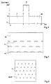
- FIG. 4 illustrates the evolution over time of gas flow rates injected into an epitaxy reactor during the formation of quantum dots.
- the abscissa axis of the diagram represents the injection time t in seconds.
- the ordinate axis represents the flow rate f in cm 3 / min.
- the temperature is maintained at a constant value of between 600 and 700 ° C., for example 635 ° C.
- the pressure is maintained at a value between 0.025 and 0.040.10 5 Pa (20 to 30 torr).
- the method according to the invention begins with initial steps of cleaning and preparing the surface of monocrystalline substrate. For example, we start by growing a few monoatomic layers of silicon, by injecting silane. For example, silane diluted to 10% in hydrogen is injected for substantially 5 s at a rate of between 15 and 25 cm 3 / min, for example 20 cm 3 / min. This first step is illustrated by part I, on the left of FIG. 4.
- an injection of a gas containing germanium, for example germane is carried out to form the quantum dots.
- this injection begins with the sending of a "puff" of german.
- puff means an injection of a large amount of german for a short time.
- germane diluted to 10% in hydrogen will be injected at an average flow rate of 200 cm 3 / min, for a period of 2 s.
- the average flow rate is clearly higher than the optimal flow rate, making it possible to obtain a maximum controllable deposition rate for the reactor considered.
- the germane injection continues at the optimal rate.
- the flux is reduced to a value between 15 and 25 cm 3 / min, for example of the order of 20 cm 3 / min, for a period of 25 to 30 s, for example 28 s.
- one causes, always under the same conditions of pressure, flow and temperature, the growth of a silicon encapsulation layer.
- injected silane diluted in hydrogen serving as a carrier gas at a rate of the order of 20 cm 3 / min.
- the duration of this last step is adjusted as a function of the pressure, flow and temperature conditions so as to increase an encapsulation layer of desired thickness.
- FIG. 5 illustrates, in partial section view and schematic, the formation on a silicon substrate 40, of three successive shots of encapsulated germanium 41 drops in silicon 42, by the method according to the present invention.
- FIG. 6 illustrates, in schematic top view and partial, the state of a drop plane 41 before its encapsulation.
- the plane considered may be the first plane formed directly on the substrate 40, or any upper plane formed on an encapsulation layer 42.
- the drops 41 formed by the process according to the present invention have homogeneous dimensions and a uniform distribution on and in the silicon 40-42. This distribution is uniform both in terms of regularity of difference between the drops 42 on a given plane that density identity terms between two distinct planes.
- the present invention therefore advantageously allows to obtain, from a simple process to implement, and to relatively low temperature, quantum dots of germanium uniformly distributed regularly and reproducible over at least one plane in silicon.
- the present invention is capable of various variants and modifications which will appear to the man of art.
- the dimensions of the quantum dots which are defined by injection conditions only and of which depends on the operating wavelength of the overall device, can be changed in any suitable way.
- germanium boxes in silicon we have considered in the present description the formation of germanium boxes in silicon.
- the present invention also applies to other types of materials. We could for example proceed as described to form nucleation centers when forming a three-layer silicon oxide - silicon nitride - oxide of silicon. More specifically, the method of the invention would allow then, after a classic formation of an underlay of silicon oxide, to cause the growth of drops of silicon nitride encapsulated in silicon oxide instead of a continuous intermediate layer. This type of structure would useful in applications in which one wishes to obtain a variation of the dielectric constant or to limit the diffusion of dopants in the structure during subsequent annealing and would apply in particular to memories with low number electron.
- the method of the invention also makes it possible to introduce rare earth quantum boxes such as erbium (Er), in silicon, germanium and / or alloy substrates strained or relaxed silicon-germanium.
- rare earth quantum boxes such as erbium (Er)
- Er erbium
- the present invention also applies to training of metallic nanostructures in insulating matrices. This makes it possible to modify the dielectric constant of the insulator.
- the present invention applies to formation by chemical vapor deposition of quantum dots of any material in any substrate.
Applications Claiming Priority (2)
| Application Number | Priority Date | Filing Date | Title |
|---|---|---|---|
| FR0010346A FR2812763B1 (fr) | 2000-08-04 | 2000-08-04 | Formation de boites quantiques |
| FR0010346 | 2000-08-04 |
Publications (1)
| Publication Number | Publication Date |
|---|---|
| EP1178522A1 true EP1178522A1 (de) | 2002-02-06 |
Family
ID=8853330
Family Applications (1)
| Application Number | Title | Priority Date | Filing Date |
|---|---|---|---|
| EP01410097A Withdrawn EP1178522A1 (de) | 2000-08-04 | 2001-08-03 | Herstellung von Quantenpunkten |
Country Status (3)
| Country | Link |
|---|---|
| US (1) | US6596555B2 (de) |
| EP (1) | EP1178522A1 (de) |
| FR (1) | FR2812763B1 (de) |
Cited By (1)
| Publication number | Priority date | Publication date | Assignee | Title |
|---|---|---|---|---|
| EP1424736A1 (de) * | 2002-11-29 | 2004-06-02 | Max-Planck-Gesellschaft zur Förderung der Wissenschaften e.V. Berlin | Halbleiterstruktur für Infrarotbereich und Herstellungsverfahren |
Families Citing this family (23)
| Publication number | Priority date | Publication date | Assignee | Title |
|---|---|---|---|---|
| US6875995B2 (en) * | 2002-08-16 | 2005-04-05 | Cree, Inc. | Heterogeneous bandgap structures for semiconductor devices and manufacturing methods therefor |
| JP2004087615A (ja) * | 2002-08-23 | 2004-03-18 | Fujitsu Ltd | 半導体レーザの製造方法 |
| KR100486607B1 (ko) * | 2002-09-17 | 2005-05-03 | 주식회사 하이닉스반도체 | 양자점 형성 방법 |
| US20060055800A1 (en) * | 2002-12-18 | 2006-03-16 | Noble Device Technologies Corp. | Adaptive solid state image sensor |
| US7453129B2 (en) * | 2002-12-18 | 2008-11-18 | Noble Peak Vision Corp. | Image sensor comprising isolated germanium photodetectors integrated with a silicon substrate and silicon circuitry |
| US7643755B2 (en) * | 2003-10-13 | 2010-01-05 | Noble Peak Vision Corp. | Optical receiver comprising a receiver photodetector integrated with an imaging array |
| US6774014B1 (en) * | 2003-03-28 | 2004-08-10 | National Taiwan University | Method of fabricating spherical quantum dots device by combination of gas condensation and epitaxial technique |
| CN1312813C (zh) * | 2003-05-21 | 2007-04-25 | 中国科学院半导体研究所 | 自组织砷化铟/砷化镓盘状量子点材料的制作方法 |
| WO2005053649A1 (en) * | 2003-11-05 | 2005-06-16 | The Government Of The United States Of America As Represented By The Secretary Of Health And Human Services | Biofunctionalized quantum dots for biological imaging |
| US7884352B2 (en) * | 2003-12-16 | 2011-02-08 | Stmicroelectronics S.A. | Single-crystal semiconductor layer with heteroatomic macronetwork |
| FR2874285B1 (fr) * | 2004-08-13 | 2006-10-13 | Commissariat Energie Atomique | Procede de realisation d'empilements d'ilots de materiau semi-conducteur encapsules dans un autre materiau semi-conducteur |
| US7732237B2 (en) * | 2005-06-27 | 2010-06-08 | The Regents Of The University Of California | Quantum dot based optoelectronic device and method of making same |
| US7629661B2 (en) * | 2006-02-10 | 2009-12-08 | Noble Peak Vision Corp. | Semiconductor devices with photoresponsive components and metal silicide light blocking structures |
| US20070262296A1 (en) * | 2006-05-11 | 2007-11-15 | Matthias Bauer | Photodetectors employing germanium layers |
| US7829162B2 (en) | 2006-08-29 | 2010-11-09 | international imagining materials, inc | Thermal transfer ribbon |
| WO2009153669A2 (en) | 2008-06-17 | 2009-12-23 | National Research Council Of Canada | Atomistic quantum dots |
| US8084739B2 (en) | 2008-07-16 | 2011-12-27 | Infrared Newco., Inc. | Imaging apparatus and methods |
| US8686365B2 (en) * | 2008-07-28 | 2014-04-01 | Infrared Newco, Inc. | Imaging apparatus and methods |
| US9422159B2 (en) * | 2010-07-15 | 2016-08-23 | Leigh E. Colby | Quantum dot digital radiographic detection system |
| US9425234B2 (en) * | 2010-07-15 | 2016-08-23 | Leigh E. Colby | Quantum dot digital radiographic detection system |
| US8492746B2 (en) | 2011-09-12 | 2013-07-23 | SemiLEDs Optoelectronics Co., Ltd. | Light emitting diode (LED) dice having wavelength conversion layers |
| US9997397B2 (en) * | 2015-02-13 | 2018-06-12 | Taiwan Semiconductor Manufacturing Co., Ltd. | Semiconductor structure and manufacturing method thereof |
| DE102015108402B4 (de) | 2015-05-28 | 2021-03-18 | Infineon Technologies Ag | Halbleiterbauelemente, ein Fluidsensor und ein Verfahren zum Bilden eines Halbleiterbauelements |
Citations (1)
| Publication number | Priority date | Publication date | Assignee | Title |
|---|---|---|---|---|
| US5608229A (en) * | 1994-09-16 | 1997-03-04 | Fujitsu Limited | Quantum box semiconductor device |
Family Cites Families (14)
| Publication number | Priority date | Publication date | Assignee | Title |
|---|---|---|---|---|
| JP3149030B2 (ja) * | 1991-06-13 | 2001-03-26 | 富士通株式会社 | 半導体量子箱装置及びその製造方法 |
| DE4345229C2 (de) * | 1993-09-30 | 1998-04-09 | Reinhard Dr Schwarz | Verfahren zum Herstellen von lumineszenten Elementstrukturen und Elementstrukturen |
| US5783498A (en) * | 1996-05-28 | 1998-07-21 | Nec Corporation | Method of forming silicon dioxide film containing germanium nanocrystals |
| EP0831538A3 (de) * | 1996-09-19 | 1999-07-14 | Canon Kabushiki Kaisha | Photovoltaisches Bauelement mit einer spezifisch dotierten Schicht |
| US5976957A (en) * | 1996-10-28 | 1999-11-02 | Sony Corporation | Method of making silicon quantum wires on a substrate |
| US5850064A (en) * | 1997-04-11 | 1998-12-15 | Starfire Electronics Development & Marketing, Ltd. | Method for photolytic liquid phase synthesis of silicon and germanium nanocrystalline materials |
| US5888885A (en) * | 1997-05-14 | 1999-03-30 | Lucent Technologies Inc. | Method for fabricating three-dimensional quantum dot arrays and resulting products |
| JPH1197667A (ja) * | 1997-09-24 | 1999-04-09 | Sharp Corp | 超微粒子あるいは超細線の形成方法およびこの形成方法による超微粒子あるいは超細線を用いた半導体素子 |
| JP3854731B2 (ja) * | 1998-03-30 | 2006-12-06 | シャープ株式会社 | 微細構造の製造方法 |
| JP2000133836A (ja) * | 1998-10-22 | 2000-05-12 | Japan Science & Technology Corp | 波長可変発光素子及びその製造方法 |
| US6313017B1 (en) * | 1999-01-26 | 2001-11-06 | University Of Vermont And State Agricultural College | Plasma enhanced CVD process for rapidly growing semiconductor films |
| US6313015B1 (en) * | 1999-06-08 | 2001-11-06 | City University Of Hong Kong | Growth method for silicon nanowires and nanoparticle chains from silicon monoxide |
| US6297095B1 (en) * | 2000-06-16 | 2001-10-02 | Motorola, Inc. | Memory device that includes passivated nanoclusters and method for manufacture |
| KR101027485B1 (ko) * | 2001-02-12 | 2011-04-06 | 에이에스엠 아메리카, 인코포레이티드 | 반도체 박막 증착을 위한 개선된 공정 |
-
2000
- 2000-08-04 FR FR0010346A patent/FR2812763B1/fr not_active Expired - Fee Related
-
2001
- 2001-08-03 EP EP01410097A patent/EP1178522A1/de not_active Withdrawn
- 2001-08-03 US US09/921,642 patent/US6596555B2/en not_active Expired - Lifetime
Patent Citations (1)
| Publication number | Priority date | Publication date | Assignee | Title |
|---|---|---|---|---|
| US5608229A (en) * | 1994-09-16 | 1997-03-04 | Fujitsu Limited | Quantum box semiconductor device |
Non-Patent Citations (3)
| Title |
|---|
| ASAHI H: "SELF-ORGANIZED QUANTUM WIRES AND DOTS IN III-V SEMICONDUCTORS", ADVANCED MATERIALS,DE,VCH VERLAGSGESELLSCHAFT, WEINHEIM, vol. 9, no. 13, 3 November 1997 (1997-11-03), pages 1019 - 1026, XP000721510, ISSN: 0935-9648 * |
| BRUNHES T ET AL: "Electroluminescence of Ge/Si self-assembled quantum dots grown by chemical vapor deposition", APPLIED PHYSICS LETTERS, 18 SEPT. 2000, AIP, USA, vol. 77, no. 12, pages 1822 - 1824, XP002176313, ISSN: 0003-6951 * |
| HERNANDEZ C ET AL: "Ge/Si self-assembled quantum dots grown on Si(001) in an industrial high-pressure chemical vapor deposition reactor", JOURNAL OF APPLIED PHYSICS, 15 JULY 1999, AIP, USA, vol. 86, no. 2, pages 1145 - 1148, XP002163898, ISSN: 0021-8979 * |
Cited By (2)
| Publication number | Priority date | Publication date | Assignee | Title |
|---|---|---|---|---|
| EP1424736A1 (de) * | 2002-11-29 | 2004-06-02 | Max-Planck-Gesellschaft zur Förderung der Wissenschaften e.V. Berlin | Halbleiterstruktur für Infrarotbereich und Herstellungsverfahren |
| US7119358B2 (en) | 2002-11-29 | 2006-10-10 | Max-Planck-Gesellschaft Zur Forderung Der Wissenschaften E.V. | Semiconductor structure for use in the near infrared region and a method of manufacturing this semiconductor structure |
Also Published As
| Publication number | Publication date |
|---|---|
| US6596555B2 (en) | 2003-07-22 |
| FR2812763B1 (fr) | 2002-11-01 |
| FR2812763A1 (fr) | 2002-02-08 |
| US20020039833A1 (en) | 2002-04-04 |
Similar Documents
| Publication | Publication Date | Title |
|---|---|---|
| EP1178522A1 (de) | Herstellung von Quantenpunkten | |
| EP2255029B1 (de) | Verfahren zur herstellung von nanostrukturen auf metalloxidsubstrat und dünnfilmvorrichtung | |
| FR2648618A1 (fr) | Procede de production d'un substrat pour la croissance selective d'un cristal, procede de croissance selective d'un cristal et procede de production d'une pile solaire | |
| FR2650704A1 (fr) | Procede de fabrication par epitaxie de couches monocristallines de materiaux a parametres de mailles differents | |
| FR2604296A1 (fr) | Procede de depot de films minces semi-conducteurs composes iii-v ou ii-vi sur un substrat par decomposition thermique | |
| EP1290721A1 (de) | Verfahren zur herstellung einer galliumnitrid-schicht | |
| EP0390661A1 (de) | Verfahren zur gerichteten Modulation der Zusammensetzung oder Dotierung von Halbleitern, insbesondere zur Realisation von planaren monolithischen elektronischen Komponenten sowie Verwendung und produkte dafür | |
| EP0944916A1 (de) | Atomare drähte von grosser länge und stabilität und verfahren zum herstellen dieser drähte | |
| FR2601506A1 (fr) | Dispositif de conversion photo-electrique | |
| FR2689680A1 (fr) | Procédé de réalisation de couches minces hétéroépitaxiales et de dispositifs électroniques. | |
| EP0199638B1 (de) | Verfahren zur Herstellung auf einem Isoliersubstrat eines gerichteten einkristallinen Siliziumfilms mit lokalisierten Fehlern | |
| FR2578680A1 (fr) | Procede pour former une couche mince monocristalline de compose semi-conducteur | |
| EP3670709A1 (de) | Herstellungsverfahren einer monokristallinen struktur | |
| EP0480804B1 (de) | Verfahren zur heteroepitaktischen Züchtung von Schichten | |
| EP4070369A1 (de) | Verfahren zur herstellung eines handhabungssubstrats für eine verbundstruktur für rf-anwendungen und handhabungssubstrat | |
| US20070077734A1 (en) | Thin buffer layers for SiGe growth on mismatched substrates | |
| FR2921200A1 (fr) | Heterostructures semi-conductrices monolithiques epitaxiees et leur procede de fabrication | |
| FR2673330A1 (fr) | Procede de realisation d'un laser a semiconducteur a ruban enterre, utilisant une gravure seche pour former ce ruban, et laser obtenu par ce procede. | |
| EP0524114A1 (de) | Verfahren zur Herstellung eines Kristalles mit einem Gittergradient | |
| FR2904008A1 (fr) | NOUVEAU PROCEDE POUR LA CROISSANCE DE NITRURES D'ELEMENTS DU GROUPE IIIb. | |
| EP0202977A1 (de) | Verfahren zur Herstellung auf einem Isoliersubstrat eines gerichteten einkristallinen Siliziumfilms mit lokalisierten Fehlern | |
| FR3112238A1 (fr) | Substrat semi-conducteur avec couche d’interface nitruree | |
| WO2020127603A1 (fr) | Substrat semi-conducteur avec couche intermediaire dopee n | |
| WO2020127605A1 (fr) | SUBSTRAT SEMI-CONDUCTEUR CO-DOPE n | |
| FR2649537A1 (fr) | Dispositif optoelectronique integre incluant une diode photoluminescente |
Legal Events
| Date | Code | Title | Description |
|---|---|---|---|
| PUAI | Public reference made under article 153(3) epc to a published international application that has entered the european phase |
Free format text: ORIGINAL CODE: 0009012 |
|
| AK | Designated contracting states |
Kind code of ref document: A1 Designated state(s): DE FR GB IT Kind code of ref document: A1 Designated state(s): AT BE CH CY DE DK ES FI FR GB GR IE IT LI LU MC NL PT SE TR |
|
| AX | Request for extension of the european patent |
Free format text: AL;LT;LV;MK;RO;SI |
|
| 17P | Request for examination filed |
Effective date: 20020722 |
|
| AKX | Designation fees paid |
Free format text: DE FR GB IT |
|
| 17Q | First examination report despatched |
Effective date: 20080909 |
|
| STAA | Information on the status of an ep patent application or granted ep patent |
Free format text: STATUS: THE APPLICATION IS DEEMED TO BE WITHDRAWN |
|
| 18D | Application deemed to be withdrawn |
Effective date: 20090120 |