EP1178522A1 - Formation of Quantum Dots - Google Patents
Formation of Quantum Dots Download PDFInfo
- Publication number
- EP1178522A1 EP1178522A1 EP01410097A EP01410097A EP1178522A1 EP 1178522 A1 EP1178522 A1 EP 1178522A1 EP 01410097 A EP01410097 A EP 01410097A EP 01410097 A EP01410097 A EP 01410097A EP 1178522 A1 EP1178522 A1 EP 1178522A1
- Authority
- EP
- European Patent Office
- Prior art keywords
- substrate
- silicon
- germanium
- boxes
- material constituting
- Prior art date
- Legal status (The legal status is an assumption and is not a legal conclusion. Google has not performed a legal analysis and makes no representation as to the accuracy of the status listed.)
- Withdrawn
Links
- 239000002096 quantum dot Substances 0.000 title claims abstract description 22
- 230000015572 biosynthetic process Effects 0.000 title abstract description 10
- 239000000463 material Substances 0.000 claims abstract description 35
- 239000000758 substrate Substances 0.000 claims abstract description 32
- 229910052710 silicon Inorganic materials 0.000 claims abstract description 30
- 239000010703 silicon Substances 0.000 claims abstract description 29
- 229910052732 germanium Inorganic materials 0.000 claims abstract description 26
- GNPVGFCGXDBREM-UHFFFAOYSA-N germanium atom Chemical compound [Ge] GNPVGFCGXDBREM-UHFFFAOYSA-N 0.000 claims abstract description 26
- 238000000407 epitaxy Methods 0.000 claims abstract description 14
- 229910052581 Si3N4 Inorganic materials 0.000 claims abstract description 5
- 238000000151 deposition Methods 0.000 claims abstract description 5
- 230000008021 deposition Effects 0.000 claims abstract description 5
- 239000004065 semiconductor Substances 0.000 claims abstract description 5
- VYPSYNLAJGMNEJ-UHFFFAOYSA-N Silicium dioxide Chemical compound O=[Si]=O VYPSYNLAJGMNEJ-UHFFFAOYSA-N 0.000 claims abstract description 4
- 229910052761 rare earth metal Inorganic materials 0.000 claims abstract description 4
- 150000002910 rare earth metals Chemical class 0.000 claims abstract description 4
- HQVNEWCFYHHQES-UHFFFAOYSA-N silicon nitride Chemical compound N12[Si]34N5[Si]62N3[Si]51N64 HQVNEWCFYHHQES-UHFFFAOYSA-N 0.000 claims abstract description 4
- 229910052814 silicon oxide Inorganic materials 0.000 claims abstract description 4
- 238000000034 method Methods 0.000 claims description 26
- 229910000078 germane Inorganic materials 0.000 claims description 14
- 238000002347 injection Methods 0.000 claims description 13
- 239000007924 injection Substances 0.000 claims description 13
- 239000007789 gas Substances 0.000 claims description 10
- 229910052739 hydrogen Inorganic materials 0.000 claims description 10
- 239000001257 hydrogen Substances 0.000 claims description 10
- 230000008569 process Effects 0.000 claims description 10
- UFHFLCQGNIYNRP-UHFFFAOYSA-N Hydrogen Chemical compound [H][H] UFHFLCQGNIYNRP-UHFFFAOYSA-N 0.000 claims description 7
- 150000002431 hydrogen Chemical class 0.000 claims description 3
- XUIMIQQOPSSXEZ-UHFFFAOYSA-N Silicon Chemical compound [Si] XUIMIQQOPSSXEZ-UHFFFAOYSA-N 0.000 abstract description 28
- BLRPTPMANUNPDV-UHFFFAOYSA-N Silane Chemical compound [SiH4] BLRPTPMANUNPDV-UHFFFAOYSA-N 0.000 description 8
- 229910000077 silane Inorganic materials 0.000 description 8
- 238000005538 encapsulation Methods 0.000 description 7
- 229910021421 monocrystalline silicon Inorganic materials 0.000 description 5
- 238000005229 chemical vapour deposition Methods 0.000 description 4
- 238000009826 distribution Methods 0.000 description 4
- 230000006911 nucleation Effects 0.000 description 3
- 238000010899 nucleation Methods 0.000 description 3
- 230000003287 optical effect Effects 0.000 description 3
- JBRZTFJDHDCESZ-UHFFFAOYSA-N AsGa Chemical compound [As]#[Ga] JBRZTFJDHDCESZ-UHFFFAOYSA-N 0.000 description 2
- 125000004429 atom Chemical group 0.000 description 2
- 239000012159 carrier gas Substances 0.000 description 2
- 238000009792 diffusion process Methods 0.000 description 2
- 230000000694 effects Effects 0.000 description 2
- 230000006872 improvement Effects 0.000 description 2
- 239000002086 nanomaterial Substances 0.000 description 2
- 239000007921 spray Substances 0.000 description 2
- 229910017214 AsGa Inorganic materials 0.000 description 1
- 229910052691 Erbium Inorganic materials 0.000 description 1
- 229910001218 Gallium arsenide Inorganic materials 0.000 description 1
- 241001676635 Lepidorhombus whiffiagonis Species 0.000 description 1
- OAICVXFJPJFONN-UHFFFAOYSA-N Phosphorus Chemical compound [P] OAICVXFJPJFONN-UHFFFAOYSA-N 0.000 description 1
- 229910000577 Silicon-germanium Inorganic materials 0.000 description 1
- LEVVHYCKPQWKOP-UHFFFAOYSA-N [Si].[Ge] Chemical compound [Si].[Ge] LEVVHYCKPQWKOP-UHFFFAOYSA-N 0.000 description 1
- 229910045601 alloy Inorganic materials 0.000 description 1
- 239000000956 alloy Substances 0.000 description 1
- 238000000137 annealing Methods 0.000 description 1
- 238000004140 cleaning Methods 0.000 description 1
- 238000004581 coalescence Methods 0.000 description 1
- 150000001875 compounds Chemical class 0.000 description 1
- 238000007796 conventional method Methods 0.000 description 1
- 239000013078 crystal Substances 0.000 description 1
- 238000005137 deposition process Methods 0.000 description 1
- 238000010586 diagram Methods 0.000 description 1
- 238000010790 dilution Methods 0.000 description 1
- 239000012895 dilution Substances 0.000 description 1
- 239000002019 doping agent Substances 0.000 description 1
- 230000005274 electronic transitions Effects 0.000 description 1
- UYAHIZSMUZPPFV-UHFFFAOYSA-N erbium Chemical compound [Er] UYAHIZSMUZPPFV-UHFFFAOYSA-N 0.000 description 1
- 239000000835 fiber Substances 0.000 description 1
- 230000004907 flux Effects 0.000 description 1
- 230000006870 function Effects 0.000 description 1
- 239000012535 impurity Substances 0.000 description 1
- 239000012212 insulator Substances 0.000 description 1
- 238000004519 manufacturing process Methods 0.000 description 1
- 230000007246 mechanism Effects 0.000 description 1
- 230000015654 memory Effects 0.000 description 1
- 238000012986 modification Methods 0.000 description 1
- 230000004048 modification Effects 0.000 description 1
- 239000013307 optical fiber Substances 0.000 description 1
- RJCRUVXAWQRZKQ-UHFFFAOYSA-N oxosilicon;silicon Chemical compound [Si].[Si]=O RJCRUVXAWQRZKQ-UHFFFAOYSA-N 0.000 description 1
- 230000000737 periodic effect Effects 0.000 description 1
- 229910052698 phosphorus Inorganic materials 0.000 description 1
- 239000011574 phosphorus Substances 0.000 description 1
- 239000002243 precursor Substances 0.000 description 1
- 239000002210 silicon-based material Substances 0.000 description 1
- 230000007704 transition Effects 0.000 description 1
- 238000009827 uniform distribution Methods 0.000 description 1
Images

Classifications
-
- H—ELECTRICITY
- H01—ELECTRIC ELEMENTS
- H01L—SEMICONDUCTOR DEVICES NOT COVERED BY CLASS H10
- H01L33/00—Semiconductor devices with at least one potential-jump barrier or surface barrier specially adapted for light emission; Processes or apparatus specially adapted for the manufacture or treatment thereof or of parts thereof; Details thereof
- H01L33/02—Semiconductor devices with at least one potential-jump barrier or surface barrier specially adapted for light emission; Processes or apparatus specially adapted for the manufacture or treatment thereof or of parts thereof; Details thereof characterised by the semiconductor bodies
- H01L33/04—Semiconductor devices with at least one potential-jump barrier or surface barrier specially adapted for light emission; Processes or apparatus specially adapted for the manufacture or treatment thereof or of parts thereof; Details thereof characterised by the semiconductor bodies with a quantum effect structure or superlattice, e.g. tunnel junction
- H01L33/06—Semiconductor devices with at least one potential-jump barrier or surface barrier specially adapted for light emission; Processes or apparatus specially adapted for the manufacture or treatment thereof or of parts thereof; Details thereof characterised by the semiconductor bodies with a quantum effect structure or superlattice, e.g. tunnel junction within the light emitting region, e.g. quantum confinement structure or tunnel barrier
-
- B—PERFORMING OPERATIONS; TRANSPORTING
- B82—NANOTECHNOLOGY
- B82Y—SPECIFIC USES OR APPLICATIONS OF NANOSTRUCTURES; MEASUREMENT OR ANALYSIS OF NANOSTRUCTURES; MANUFACTURE OR TREATMENT OF NANOSTRUCTURES
- B82Y10/00—Nanotechnology for information processing, storage or transmission, e.g. quantum computing or single electron logic
-
- H—ELECTRICITY
- H01—ELECTRIC ELEMENTS
- H01L—SEMICONDUCTOR DEVICES NOT COVERED BY CLASS H10
- H01L21/00—Processes or apparatus adapted for the manufacture or treatment of semiconductor or solid state devices or of parts thereof
- H01L21/02—Manufacture or treatment of semiconductor devices or of parts thereof
- H01L21/02104—Forming layers
- H01L21/02365—Forming inorganic semiconducting materials on a substrate
- H01L21/02367—Substrates
- H01L21/0237—Materials
- H01L21/02373—Group 14 semiconducting materials
- H01L21/02381—Silicon, silicon germanium, germanium
-
- H—ELECTRICITY
- H01—ELECTRIC ELEMENTS
- H01L—SEMICONDUCTOR DEVICES NOT COVERED BY CLASS H10
- H01L21/00—Processes or apparatus adapted for the manufacture or treatment of semiconductor or solid state devices or of parts thereof
- H01L21/02—Manufacture or treatment of semiconductor devices or of parts thereof
- H01L21/02104—Forming layers
- H01L21/02365—Forming inorganic semiconducting materials on a substrate
- H01L21/02436—Intermediate layers between substrates and deposited layers
- H01L21/02439—Materials
- H01L21/02441—Group 14 semiconducting materials
- H01L21/0245—Silicon, silicon germanium, germanium
-
- H—ELECTRICITY
- H01—ELECTRIC ELEMENTS
- H01L—SEMICONDUCTOR DEVICES NOT COVERED BY CLASS H10
- H01L21/00—Processes or apparatus adapted for the manufacture or treatment of semiconductor or solid state devices or of parts thereof
- H01L21/02—Manufacture or treatment of semiconductor devices or of parts thereof
- H01L21/02104—Forming layers
- H01L21/02365—Forming inorganic semiconducting materials on a substrate
- H01L21/02436—Intermediate layers between substrates and deposited layers
- H01L21/02494—Structure
- H01L21/02496—Layer structure
- H01L21/02505—Layer structure consisting of more than two layers
-
- H—ELECTRICITY
- H01—ELECTRIC ELEMENTS
- H01L—SEMICONDUCTOR DEVICES NOT COVERED BY CLASS H10
- H01L21/00—Processes or apparatus adapted for the manufacture or treatment of semiconductor or solid state devices or of parts thereof
- H01L21/02—Manufacture or treatment of semiconductor devices or of parts thereof
- H01L21/02104—Forming layers
- H01L21/02365—Forming inorganic semiconducting materials on a substrate
- H01L21/02436—Intermediate layers between substrates and deposited layers
- H01L21/02494—Structure
- H01L21/02513—Microstructure
-
- H—ELECTRICITY
- H01—ELECTRIC ELEMENTS
- H01L—SEMICONDUCTOR DEVICES NOT COVERED BY CLASS H10
- H01L21/00—Processes or apparatus adapted for the manufacture or treatment of semiconductor or solid state devices or of parts thereof
- H01L21/02—Manufacture or treatment of semiconductor devices or of parts thereof
- H01L21/02104—Forming layers
- H01L21/02365—Forming inorganic semiconducting materials on a substrate
- H01L21/02518—Deposited layers
- H01L21/02521—Materials
- H01L21/02524—Group 14 semiconducting materials
- H01L21/02532—Silicon, silicon germanium, germanium
-
- H—ELECTRICITY
- H01—ELECTRIC ELEMENTS
- H01L—SEMICONDUCTOR DEVICES NOT COVERED BY CLASS H10
- H01L21/00—Processes or apparatus adapted for the manufacture or treatment of semiconductor or solid state devices or of parts thereof
- H01L21/02—Manufacture or treatment of semiconductor devices or of parts thereof
- H01L21/02104—Forming layers
- H01L21/02365—Forming inorganic semiconducting materials on a substrate
- H01L21/02612—Formation types
- H01L21/02617—Deposition types
- H01L21/0262—Reduction or decomposition of gaseous compounds, e.g. CVD
-
- H—ELECTRICITY
- H01—ELECTRIC ELEMENTS
- H01L—SEMICONDUCTOR DEVICES NOT COVERED BY CLASS H10
- H01L29/00—Semiconductor devices adapted for rectifying, amplifying, oscillating or switching, or capacitors or resistors with at least one potential-jump barrier or surface barrier, e.g. PN junction depletion layer or carrier concentration layer; Details of semiconductor bodies or of electrodes thereof ; Multistep manufacturing processes therefor
- H01L29/02—Semiconductor bodies ; Multistep manufacturing processes therefor
- H01L29/12—Semiconductor bodies ; Multistep manufacturing processes therefor characterised by the materials of which they are formed
- H01L29/122—Single quantum well structures
- H01L29/127—Quantum box structures
-
- H—ELECTRICITY
- H01—ELECTRIC ELEMENTS
- H01L—SEMICONDUCTOR DEVICES NOT COVERED BY CLASS H10
- H01L33/00—Semiconductor devices with at least one potential-jump barrier or surface barrier specially adapted for light emission; Processes or apparatus specially adapted for the manufacture or treatment thereof or of parts thereof; Details thereof
- H01L33/005—Processes
- H01L33/0054—Processes for devices with an active region comprising only group IV elements
-
- Y—GENERAL TAGGING OF NEW TECHNOLOGICAL DEVELOPMENTS; GENERAL TAGGING OF CROSS-SECTIONAL TECHNOLOGIES SPANNING OVER SEVERAL SECTIONS OF THE IPC; TECHNICAL SUBJECTS COVERED BY FORMER USPC CROSS-REFERENCE ART COLLECTIONS [XRACs] AND DIGESTS
- Y10—TECHNICAL SUBJECTS COVERED BY FORMER USPC
- Y10S—TECHNICAL SUBJECTS COVERED BY FORMER USPC CROSS-REFERENCE ART COLLECTIONS [XRACs] AND DIGESTS
- Y10S438/00—Semiconductor device manufacturing: process
- Y10S438/962—Quantum dots and lines
-
- Y—GENERAL TAGGING OF NEW TECHNOLOGICAL DEVELOPMENTS; GENERAL TAGGING OF CROSS-SECTIONAL TECHNOLOGIES SPANNING OVER SEVERAL SECTIONS OF THE IPC; TECHNICAL SUBJECTS COVERED BY FORMER USPC CROSS-REFERENCE ART COLLECTIONS [XRACs] AND DIGESTS
- Y10—TECHNICAL SUBJECTS COVERED BY FORMER USPC
- Y10S—TECHNICAL SUBJECTS COVERED BY FORMER USPC CROSS-REFERENCE ART COLLECTIONS [XRACs] AND DIGESTS
- Y10S977/00—Nanotechnology
- Y10S977/70—Nanostructure
- Y10S977/701—Integrated with dissimilar structures on a common substrate
- Y10S977/72—On an electrically conducting, semi-conducting, or semi-insulating substrate
- Y10S977/721—On a silicon substrate
-
- Y—GENERAL TAGGING OF NEW TECHNOLOGICAL DEVELOPMENTS; GENERAL TAGGING OF CROSS-SECTIONAL TECHNOLOGIES SPANNING OVER SEVERAL SECTIONS OF THE IPC; TECHNICAL SUBJECTS COVERED BY FORMER USPC CROSS-REFERENCE ART COLLECTIONS [XRACs] AND DIGESTS
- Y10—TECHNICAL SUBJECTS COVERED BY FORMER USPC
- Y10S—TECHNICAL SUBJECTS COVERED BY FORMER USPC CROSS-REFERENCE ART COLLECTIONS [XRACs] AND DIGESTS
- Y10S977/00—Nanotechnology
- Y10S977/84—Manufacture, treatment, or detection of nanostructure
- Y10S977/89—Deposition of materials, e.g. coating, cvd, or ald
- Y10S977/891—Vapor phase deposition
Abstract
Description
La présente invention concerne la fabrication de "boítes quantiques" d'un premier matériau dans un second matériau semiconducteur. Plus particulièrement, la présente invention concerne la réalisation de boítes quantiques dans un substrat de silicium.The present invention relates to the manufacture of "quantum dots" of a first material in a second material semiconductor. More particularly, the present invention concerns the realization of quantum dots in a substrate of silicon.
De telles boítes quantiques sont, par exemple, décrites dans le document "Ge/Si self-assembled quantum dots grown on Si (100) in an industrial high-pressure chemical vapor deposition reactor" de C. Hernandez, Y. Campidelli, D. Simon, D. Bensahel, I. Sagnes, G. Patriarche, P. Boucaus et S. Sauvage, paru dans J. Appl. Phys., 86/2, 1999, 1145-1148. Elles sont utilisées dans de très nombreux domaines d'application. On considère ci-après à titre d'exemple non-limitatif le domaine des télécommunications.Such quantum dots are, for example, described in the document "Ge / Si self-assembled quantum dots grown on Si (100) in an industrial high-pressure chemical vapor deposition reactor "by C. Hernandez, Y. Campidelli, D. Simon, D. Bensahel, I. Sagnes, G. Patriarche, P. Boucaus and S. Sauvage, published in J. Appl. Phys., 86/2, 1999, 1145-1148. They are used in many fields of application. We consider below By way of non-limiting example, the field of telecommunications.
Dans le domaine des télécommunications, on utilise de façon croissante des systèmes à base de fibres optiques. Pour ce faire, on recourt à des émetteurs propres à convertir une différence de potentiel en un signal lumineux et à des récepteurs propres à convertir un signal lumineux transmis par une fibre optique en un signal électrique. Le signal lumineux émis et/ou reçu est généralement situé dans une plage de longueurs d'onde comprise entre 1,4 et 1,5 µm. In the telecommunications field, we use growing systems based on optical fibers. For this we use transmitters capable of converting a difference potential in a light signal and to receivers suitable for converting a light signal transmitted by a fiber optical signal. The light signal emitted and / or received is usually in a wavelength range between 1.4 and 1.5 µm.
Jusqu'à une période récente, on a utilisé, pour réaliser de tels récepteurs et/ou émetteurs, des combinaisons de matériaux des colonnes III et V de la classification périodique des éléments. Par exemple, l'arséniure de gallium (AsGa) ou l'indiure de phosphore (InP).Until recently, we used to realize such receivers and / or transmitters, combinations of materials of columns III and V of the periodic table elements. For example, gallium arsenide (AsGa) or phosphorus indide (InP).
On préférerait toutefois utiliser pour les émetteurs et récepteurs optiques des matériaux à base de silicium, mais le recours au silicium pose différents problèmes. Tout d'abord l'intervalle de bande d'énergie du silicium entre ses bandes de valence et de conduction est relativement faible et les transitions sont de type "indirect". Par "indirect", on entend que le passage d'un électron de la bande de valence à la bande de conduction se fait en plusieurs sauts et non en un seul saut comme dans le cas des composés III-V. Le silicium est alors presque inutilisable comme émetteur, c'est-à-dire convertisseur d'énergie électrique en énergie lumineuse. En effet, du fait du caractère indirect des transitions électroniques, celles-ci sont fortement dissipatrices et très faiblement émettrices. En outre, l'intervalle de bande d'énergie relativement faible, de l'ordre de 1,1 eV, correspond à une émission de photons d'une longueur d'onde inférieure à 1 µm, peu utilisée dans le domaine des télécommunications.We would however prefer to use for transmitters and optical receptors for silicon-based materials but the using silicon poses different problems. First of all the energy band gap of silicon between its bands of valence and conduction is relatively low and the transitions are of the "indirect" type. By "indirect" is meant that the passage of an electron from the valence band to the band conduction is done in several jumps and not in a single jump as in the case of the III-V compounds. The silicon is then almost unusable as a transmitter, i.e. converter from electric energy to light energy. Because of the indirect nature of electronic transitions, these are strongly dissipative and very weakly emitting. In addition, the relatively low energy band gap, on the order 1.1 eV, corresponds to a photon emission of a length wave less than 1 µm, little used in the telecommunications field.
On a donc proposé d'améliorer les propriétés optiques, c'est-à-dire d'émission et de réception, du silicium en formant dans celui-ci des boítes quantiques.It has therefore been proposed to improve the optical properties, that is to say emission and reception, of the silicon by forming in this one quantum boxes.
La figure 1 illustre, en vue en coupe partielle et schématique, une boíte quantique telle que décrite, par exemple, dans l'article susmentionné du Journal of Applied Physics. Cette boíte B est constituée d'un ílot de germanium formé sur un substrat S de silicium monocristallin. Bien que théoriquement on souhaite former un cube parfait d'une arête inférieure à 50 nm, on réalise en pratique une nanostructure en forme de dôme ou goutte B, présentant une base L et une hauteur h. En pratique, on parvient à réaliser de telles boítes de base L comprise entre 20 et 50 nm, et de hauteur comprise entre 6 et 30 nm. La boíte B est encapsulée dans une couche de silicium monocristallin.Figure 1 illustrates, in partial sectional view and schematic, a quantum dot as described, for example, in the aforementioned article from the Journal of Applied Physics. This box B consists of a germanium island formed on a substrate S of monocrystalline silicon. Although theoretically we wishes to form a perfect cube with an edge less than 50 nm, in practice, a dome-shaped nanostructure is produced or drop B, having a base L and a height h. In practice, we manages to make such basic boxes L between 20 and 50 nm, and between 6 and 30 nm in height. Box B is encapsulated in a layer of monocrystalline silicon.
Dans de nombreuses applications, pour obtenir des performances acceptables, par exemple un émetteur/récepteur d'une émissivité/réceptivité convenable, il est souhaitable de pouvoir réaliser plusieurs plans superposés contenant chacun plusieurs boítes similaires à celles de la figure 1.In many applications, to obtain acceptable performance, for example a transmitter / receiver of a emissivity / suitable receptivity, it is desirable to be able to create several superimposed plans, each containing several boxes similar to those in Figure 1.
Comme l'expose l'article cité précédemment, la formation de dômes ou gouttes résulte d'un mécanisme de contrainte entre des mailles cristallographiques de dimensions différentes, mais relativement voisines, de deux semiconducteurs. On a montré que ce procédé de croissance, dit de Stranski-Krastanow, provoque, par exemple, la formation de gouttes de germanium sur du silicium à partir de divers procédés de dépôt comprenant des épitaxies moléculaires, des dépôts chimiques en phase vapeur sous faible pression, ou des dépôts chimiques en phase vapeur sous vide important.As explained in the article cited above, training domes or drops result from a constraint mechanism between crystallographic meshes of different dimensions, but relatively similar, of two semiconductors. We showed that this growth process, known as Stranski-Krastanow, causes, for example, the formation of germanium drops on silicon from various deposition processes including molecular epitaxy, chemical vapor deposition under low pressure, or chemical vapor deposition under significant vacuum.
Plus particulièrement, pour former des boítes quantiques de germanium dans du silicium on effectue, par exemple, une épitaxie par injection continue de germane (GeH4), sur un substrat de silicium monocristallin. Alors, les quelques premières épaisseurs atomiques déposées forment une couche dont la surface est régulière mais non plane. En raison des contraintes liées aux différences des réseaux cristallins, la surface présente une allure "ondulatoire" de type sinusoïdal. En d'autres termes, la surface supérieure d'une couche de germanium de quelques épaisseurs atomiques, formée sur du silicium, présente des creux et des bosses répartis de façon régulière. L'injection de germane se poursuivant, les contraintes cristallographiques - déformations du réseau naturel du germanium - provoquent la croissance de gouttes ou boítes similaires à celles de la figure 1. Cette injection doit être interrompue quand les gouttes ou boítes ont atteint une dimension souhaitée, avant que ne se produise une coalescence des gouttes, puis la formation d'une couche continue contenant des dislocations. More particularly, to form quantum dots of germanium in silicon, epitaxy is carried out, for example, by continuous injection of germane (GeH 4 ), on a monocrystalline silicon substrate. Then, the first few atomic thicknesses deposited form a layer whose surface is regular but not planar. Due to the constraints linked to the differences in crystal lattices, the surface has a sinusoidal "wave" shape. In other words, the upper surface of a germanium layer of a few atomic thicknesses, formed on silicon, has hollows and bumps distributed evenly. The injection of germane continuing, the crystallographic constraints - deformations of the natural network of germanium - cause the growth of drops or boxes similar to those of FIG. 1. This injection must be stopped when the drops or boxes have reached a desired dimension, before a coalescence of the drops occurs, then the formation of a continuous layer containing dislocations.
On procède ensuite à une croissance épitaxiale d'une couche de silicium qui encapsule les boítes de germanium.We then proceed to an epitaxial growth of one layer of silicon which encapsulates the germanium boxes.
La figure 2 illustre, en vue en coupe partielle et
schématique, le résultat de la mise en oeuvre répétée d'un tel
procédé. Par exemple, on a formé, sur un substrat de silicium 20,
trois plans sensiblement horizontaux de gouttes de germanium
(boítes quantiques) 21 encapsulées dans du silicium 22.FIG. 2 illustrates, in partial section view and
schematic, the result of the repeated implementation of such
process. For example, on a
La figure 3 illustre, en vue de dessus partielle et
schématique, l'un quelconque des plans de gouttes 21.Figure 3 illustrates, in partial top view and
schematic, any of the
On cherche à obtenir des densités de boítes aussi élevées que possible (≥ 1010 cm-2) et une répartition de taille aussi fixe que possible. Toutefois, comme l'illustrent très schématiquement les figures 2 et 3, la mise en oeuvre courante du procédé de croissance contrainte de Stranski-Krastanow conduit à des structures de gouttes hétérogènes tant en ce qui concerne la répartition des gouttes que leur taille. Pour faire ressortir toutes les difficultés de mise en oeuvre de ce procédé, on va rappeler les principales étapes de réalisation de l'épitaxie en phase gazeuse de gouttes de germanium sur un substrat de silicium.We seek to obtain densities of boxes as high as possible (≥ 10 10 cm -2 ) and a size distribution as fixed as possible. However, as illustrated very diagrammatically in FIGS. 2 and 3, the current implementation of the constrained growth process of Stranski-Krastanow leads to heterogeneous drop structures both as regards the distribution of the drops as their size. To bring out all the difficulties in implementing this method, we will recall the main stages in the epitaxy in the gas phase of germanium drops on a silicon substrate.
Tout d'abord, l'état de surface du substrat de silicium joue un rôle important. On pense actuellement qu'il faut trouver un compromis optimal entre une homogénéité parfaite et une certaine répartition de défauts.First, the surface condition of the silicon substrate play an important role. We currently think we have to find an optimal compromise between perfect homogeneity and a certain distribution of faults.
On s'aperçoit aussi que le choix des conditions de l'épitaxie doit satisfaire à un compromis. En effet, ces conditions doivent être choisies pour que l'épitaxie ne soit pas trop lente car, dans ce cas, les risques liés à la présence d'inévitables impuretés (apportées par les précurseurs gazeux et/ou liées au taux de fuite du réacteur) augmentent. Par contre, si la vitesse de croissance des gouttes de germanium est trop importante le processus devient difficilement contrôlable. En effet, cette croissance doit être interrompue de façon précise comme on l'a indiqué précédemment. We also notice that the choice of the conditions of epitaxy must satisfy a compromise. Indeed, these conditions must be chosen so that the epitaxy is not too much slow because, in this case, the risks linked to the presence of inevitable impurities (brought by gaseous precursors and / or related to the reactor leakage rate) increase. However, if the growth rate of germanium drops is too high the process becomes difficult to control. Indeed, this growth must be stopped precisely as we said earlier.
Ainsi, on définit pour des conditions données de pression, de débit, et de dilution des gaz, dans un réacteur d'épitaxie de type donné, une température "optimale" qui correspond à une vitesse de croissance "contrôlable" maximum, c'est-à-dire une vitesse aussi rapide que possible pour éviter les défauts susmentionnés, et suffisamment lente pour permettre d'interrompre l'épitaxie de façon précise à un stade souhaité (par exemple quelques dizaines de couches monoatomiques).Thus, we define for given pressure conditions, flow, and gas dilution, in an epitaxy reactor of given type, an "optimal" temperature which corresponds to a maximum "controllable" growth rate, that is to say a speed as fast as possible to avoid faults mentioned above, and slow enough to interrupt epitaxy precisely at a desired stage (e.g. a few dozen monoatomic layers).
A titre d'exemple, une séquence typique de mise en oeuvre d'un procédé de Stranski-Krastanow à une température de l'ordre de 650°C (630 à 670°C) et à une pression comprise entre 0,02 et 0,04.105 Pa (20 à 30 torr) comprend, en partant d'un substrat de silicium monocristallin, les étapes suivantes :
- injecter du silane dilué à 10 % dans de l'hydrogène pendant sensiblement 5 s, d'où il résulte la croissance de sensiblement de deux à trois monocouches de silicium monocristallin (étape optionnelle) ;
- injecter du germane dilué à 10 % dans de l'hydrogène pendant sensiblement 30 s, d'où il résulte la croissance de "gouttes" de germanium d'une hauteur correspondant à un empilement d'une trentaine d'atomes ; et
- réinjecter du silane de façon à former une couche d'encapsulation.
- injecting silane diluted to 10% in hydrogen for approximately 5 s, from which there results the growth of substantially from two to three monocrystalline silicon monolayers (optional step);
- injecting germane diluted to 10% in hydrogen for substantially 30 s, resulting in the growth of "drops" of germanium of a height corresponding to a stack of about thirty atoms; and
- reinject silane so as to form an encapsulation layer.
Selon cette séquence classique, les injections de silane et de germane sont effectuées successivement à des débits voisins. L'hydrogène (gaz porteur) est injecté à un débit d'environ 10 l/mn. Le débit des gaz injectés est maintenu généralement entre 15 et 25 cm3/mn, typiquement de l'ordre de 20 cm3/mn. Ce débit est choisi comme on l'a expliqué précédemment pour obtenir une vitesse de dépôt contrôlable maximum.According to this conventional sequence, the silane and germane injections are carried out successively at similar flow rates. The hydrogen (carrier gas) is injected at a flow rate of approximately 10 l / min. The flow rate of the injected gases is generally maintained between 15 and 25 cm 3 / min, typically of the order of 20 cm 3 / min. This flow rate is chosen as explained above to obtain a maximum controllable deposition rate.
La présente invention vise à proposer un procédé de croissance de boítes quantiques propre à former des boítes régulières, agencées de façon homogène sur un substrat.The present invention aims to provide a method of growth of quantum boxes suitable for forming regular boxes, arranged homogeneously on a substrate.
La présente invention vise également à proposer un tel procédé qui soit reproductible. The present invention also aims to provide such a process that is reproducible.
Pour atteindre ces objets, la présente invention prévoit un procédé de formation, sur un substrat semiconducteur monocristallin d'un premier matériau, de boítes quantiques en un second matériau, consistant à faire croítre par épitaxie en phase gazeuse le second matériau sur le premier matériau dans des conditions optimales propres à assurer une croissance à une vitesse contrôlable maximum, et comportant une étape initiale consistant à envoyer sur le substrat une bouffée d'un gaz comprenant le second matériau, dans des conditions correspondant à une vitesse de dépôt nettement plus rapide que ladite vitesse contrôlable maximum.To achieve these objects, the present invention provides a formation process, on a semiconductor substrate monocrystalline of a first material, of quantum boxes in one second material, consisting of growing by phase epitaxy gaseous the second material on the first material in optimal conditions to ensure growth at a maximum controllable speed, including an initial step consisting in sending a puff of gas onto the substrate comprising the second material, under corresponding conditions at a deposition speed significantly faster than said speed maximum controllable.
Selon un mode de réalisation de la présente invention, le premier matériau constituant le substrat est du silicium et le second matériau constituant les boítes est du germanium.According to an embodiment of the present invention, the first material constituting the substrate is silicon and the second material constituting the boxes is germanium.
Selon un mode de réalisation de la présente invention, le procédé est mis en oeuvre dans un réacteur d'épitaxie à une température de 630 à 670°C à une pression de 0,02 à 0,04 105 Pa, lesdites conditions optimales correspondant à un débit de l'ordre de 15 à 25 cm3/mn de germane dilué à 10 % dans de l'hydrogène, et l'étape initiale consistant à envoyer une bouffée de germane dilué à 10 % dans de l'hydrogène à un débit de l'ordre de 200 cm3/mn pendant une durée de 1 à 5 s.According to one embodiment of the present invention, the method is implemented in an epitaxy reactor at a temperature of 630 to 670 ° C at a pressure of 0.02 to 0.04 10 5 Pa, said optimal conditions corresponding at a flow rate of the order of 15 to 25 cm 3 / min of germane diluted to 10% in hydrogen, and the initial step consisting in sending a burst of germane diluted to 10% in hydrogen to a flow rate of the order of 200 cm 3 / min for a period of 1 to 5 s.
Selon un mode de réalisation de la présente invention, l'étape initiale d'envoi d'une bouffée est suivie d'une injection de germane dans lesdites conditions optimales pendant 25 à 40 s.According to an embodiment of the present invention, the initial stage of sending a puff is followed by an injection of germane under said optimal conditions for 25 to 40 s.
Selon un mode de réalisation de la présente invention, le premier matériau constituant le substrat est du silicium ou du germanium et le second matériau constituant les boítes est une terre rare.According to an embodiment of the present invention, the first material constituting the substrate is silicon or germanium and the second material making up the boxes is a rare earth.
Selon un mode de réalisation de la présente invention, le premier matériau constituant le substrat est de l'oxyde de silicium et le second matériau constituant les boítes est du nitrure de silicium.According to an embodiment of the present invention, the first material constituting the substrate is oxide of silicon and the second material constituting the boxes is silicon nitride.
Ces objets, caractéristiques et avantages, ainsi que
d'autres de la présente invention seront exposés en détail dans
la description suivante de modes de réalisation particuliers
faite à titre non-limitatif en relation avec les figures jointes
parmi lesquelles :
Par souci de clarté, les mêmes éléments ont été désignés par les mêmes références aux différentes figures et, de plus, comme cela est habituel dans la représentation des circuits intégrés, les diverses figures ne sont pas tracées à l'échelle.For the sake of clarity, the same elements have been designated by the same references to the different figures and, from more, as is usual in the representation of circuits integrated, the various figures are not drawn to scale.
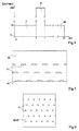
Le procédé selon l'invention sera exposé ci-après en relation avec la figure 4 qui illustre l'évolution au cours du temps de débits de gaz injectés dans un réacteur d'épitaxie pendant la formation de boítes quantiques. L'axe des abscisses du diagramme représente la durée d'injection t en secondes. L'axe des ordonnées représente le débit f en cm3/mn.The method according to the invention will be explained below in relation to FIG. 4 which illustrates the evolution over time of gas flow rates injected into an epitaxy reactor during the formation of quantum dots. The abscissa axis of the diagram represents the injection time t in seconds. The ordinate axis represents the flow rate f in cm 3 / min.
On considère à titre d'exemple non-limitatif que la température est maintenue à une valeur constante comprise entre 600 et 700°C, par exemple 635°C. De même on considère que la pression est maintenue à une valeur comprise entre 0,025 et 0,040.105 Pa (20 à 30 torr).It is considered by way of non-limiting example that the temperature is maintained at a constant value of between 600 and 700 ° C., for example 635 ° C. Similarly, it is considered that the pressure is maintained at a value between 0.025 and 0.040.10 5 Pa (20 to 30 torr).
Le procédé selon l'invention commence par des étapes initiales de nettoyage et de préparation de la surface de substrat monocristallin. Par exemple, on commence par faire croítre quelques couches monoatomiques de silicium, par injection de silane. On injecte par exemple du silane dilué à 10 % dans de l'hydrogène pendant sensiblement 5 s à un débit compris entre 15 et 25 cm3/mn, par exemple 20 cm3/mn. Cette première étape est illustrée par la partie I, à gauche de la figure 4.The method according to the invention begins with initial steps of cleaning and preparing the surface of monocrystalline substrate. For example, we start by growing a few monoatomic layers of silicon, by injecting silane. For example, silane diluted to 10% in hydrogen is injected for substantially 5 s at a rate of between 15 and 25 cm 3 / min, for example 20 cm 3 / min. This first step is illustrated by part I, on the left of FIG. 4.
Ensuite, on effectue une injection d'un gaz contenant du germanium, par exemple du germane, pour former les boítes quantiques. Toutefois, selon l'invention, cette injection commence par l'envoi d'une "bouffée" de germane. Par bouffée, on entend une injection d'une quantité élevée de germane pendant un temps bref. Par exemple, on injectera du germane dilué à 10 % dans de l'hydrogène à un débit moyen de 200 cm3/mn, pendant une durée de 2 s. Cette bouffée est illustrée par la partie centrale II de la figure 4, comprise entre les instants t = 5 et 7 s. Pendant cette bouffée, le débit moyen est nettement supérieur au débit optimal, permettant d'obtenir une vitesse de dépôt contrôlable maximum pour le réacteur considéré.Next, an injection of a gas containing germanium, for example germane, is carried out to form the quantum dots. However, according to the invention, this injection begins with the sending of a "puff" of german. By puff means an injection of a large amount of german for a short time. For example, germane diluted to 10% in hydrogen will be injected at an average flow rate of 200 cm 3 / min, for a period of 2 s. This puff is illustrated by the central part II of FIG. 4, between the instants t = 5 and 7 s. During this puff, the average flow rate is clearly higher than the optimal flow rate, making it possible to obtain a maximum controllable deposition rate for the reactor considered.
Ensuite, l'injection de germane se poursuit au débit optimal. Le flux est ramené à une valeur comprise entre 15 et 25 cm3/mn, par exemple de l'ordre de 20 cm3/mn, pendant une durée de 25 à 30 s, par exemple de 28 s. Le débit et la durée sont ajustés de façon à faire croítre les quelques dizaines d'épaisseurs atomiques désirées des gouttes ou boítes quantiques de germanium. Cette étape de croissance des gouttes est illustrée par la partie III à droite de la figure 4, comprise entre t = 7 s et t = 35 s.Then, the germane injection continues at the optimal rate. The flux is reduced to a value between 15 and 25 cm 3 / min, for example of the order of 20 cm 3 / min, for a period of 25 to 30 s, for example 28 s. The flow rate and the duration are adjusted so as to increase the few tens of atomic thicknesses desired of the quantum drips or boxes of germanium. This drop growth step is illustrated by part III on the right of FIG. 4, between t = 7 s and t = 35 s.
Enfin, on provoque, toujours dans les mêmes conditions de pression, de débit et de température, la croissance d'une couche d'encapsulation de silicium. Par exemple, on injecte du silane dilué dans de l'hydrogène servant de gaz porteur à un débit de l'ordre de 20 cm3/mn. La durée de cette dernière étape est ajustée en fonction des conditions de pression, de débit et de température de façon à faire croítre une couche d'encapsulation d'épaisseur voulue. Finally, one causes, always under the same conditions of pressure, flow and temperature, the growth of a silicon encapsulation layer. For example, injected silane diluted in hydrogen serving as a carrier gas at a rate of the order of 20 cm 3 / min. The duration of this last step is adjusted as a function of the pressure, flow and temperature conditions so as to increase an encapsulation layer of desired thickness.
La séquence précédente d'étapes successives d'envoi d'une bouffée de germane, d'injection de germane à débit "optimal" et de croissance d'une couche d'encapsulation de silicium, peut ensuite être éventuellement répétée de façon à former autant de plans que nécessaire.The previous sequence of successive sending steps a whiff of german, germane injection at a rate "optimal" and growth of a silicon encapsulation layer, can then be optionally repeated to form as many plans as necessary.
La figure 5 illustre, en vue en coupe partielle et
schématique, la formation sur un substrat de silicium 40, de
trois plans successifs de gouttes de germanium 41 encapsulées
dans du silicium 42, par le procédé selon la présente invention.FIG. 5 illustrates, in partial section view and
schematic, the formation on a
La figure 6 illustre, en vue de dessus schématique et
partielle, l'état d'un plan de gouttes 41 avant son encapsulation.
Le plan considéré peut être le premier plan formé
directement sur le substrat 40, ou un quelconque plan supérieur
formé sur une couche d'encapsulation 42.FIG. 6 illustrates, in schematic top view and
partial, the state of a
Comme l'illustrent les figures 5 et 6, les gouttes 41
formées par le procédé selon la présente invention présentent des
dimensions homogènes et une répartition uniforme sur et dans le
silicium 40-42. Cette répartition est uniforme tant en termes de
régularité d'écart entre les gouttes 42 sur un plan donné qu'en
termes d'identité de densité entre deux plans distincts.As illustrated in FIGS. 5 and 6, the
Cette amélioration a été constatée expérimentalement, sans qu'elle soit expliquée de manière théorique. Sans que cela constitue une limitation de l'invention, on peut penser que les améliorations ainsi observées sont dues à la détente très rapide et importante de la bouffée initiale. En effet, en moins de cinq secondes, une forte quantité de gaz comprenant le germanium passe de la pression atmosphérique à la pression nettement inférieure de la chambre d'épitaxie. On peut supposer qu'une telle détente provoque un effet de pulvérisation ("spray") qui limite la diffusion du germanium à la surface du substrat. Cet effet de pulvérisation ne laisserait donc pas le temps aux atomes de germanium de diffuser et de s'organiser à la surface du substrat de façon à former une couche régulière. Par contre, il provoquerait une nucléation forcée par un "collage" homogène du germanium sur le substrat, les points de collage constituant autant de points de nucléation lors de la croissance régulière ultérieure. La reproductibilité de la structure dépend alors de la reproductibilité de la bouffée initiale.This improvement has been observed experimentally, without being explained theoretically. Without that constitutes a limitation of the invention, it may be thought that the improvements thus observed are due to very rapid relaxation and significant of the initial puff. Indeed, in less than five seconds, a large amount of gas including germanium passes from atmospheric pressure to much lower pressure of the epitaxy chamber. We can assume that such relaxation causes a spray effect which limits the diffusion germanium on the surface of the substrate. This spray effect would therefore not give the germanium atoms time to diffuse and organize itself on the surface of the substrate so as to form a regular layer. However, it would cause forced nucleation by a homogeneous "bonding" of germanium on the substrate, the bonding points constituting as many points of nucleation during subsequent regular growth. Reproducibility of the structure then depends on the reproducibility of the initial puff.
La présente invention permet donc avantageusement d'obtenir, à partir d'un procédé simple à mettre en oeuvre, et à relativement basse température, des boítes quantiques de germanium réparties de façon homogène régulière et reproductible sur au moins un plan dans du silicium.The present invention therefore advantageously allows to obtain, from a simple process to implement, and to relatively low temperature, quantum dots of germanium uniformly distributed regularly and reproducible over at least one plane in silicon.
Les avantages obtenus en termes d'applications sont multiples. Par exemple, dans le domaine des télécommunications, il est possible de former ainsi des dispositifs suffisamment sensibles et dans un domaine de longueurs d'ondes adéquat pour constituer des émetteurs. Les dispositifs obtenus à l'aide d'un procédé classique ne pouvaient par contre être utilisés que comme détecteurs. Par rapport à ces détecteurs classiques, ceux obtenus à l'aide du procédé selon la présente invention présentent une détectivité améliorée.The advantages obtained in terms of applications are multiple. For example, in the telecommunications field, it is possible to form devices sufficiently sensitive and in a suitable wavelength range for constitute issuers. The devices obtained using a conventional process could only be used as detectors. Compared to these conventional detectors, those obtained using the method according to the present invention have a improved detectivity.
Bien entendu, la présente invention est susceptible de diverses variantes et modifications qui apparaítront à l'homme de l'art. En particulier, les dimensions des boítes quantiques, qui sont définies par les seules conditions d'injection et dont dépend la longueur d'onde de fonctionnement du dispositif global, peuvent être modifiées de toute façon appropriée.Of course, the present invention is capable of various variants and modifications which will appear to the man of art. In particular, the dimensions of the quantum dots, which are defined by injection conditions only and of which depends on the operating wavelength of the overall device, can be changed in any suitable way.
Par ailleurs, on a considéré dans la présente description la formation de boítes de germanium dans du silicium. Toutefois, la présente invention s'applique également à d'autres types de matériaux. On pourra par exemple procéder de la façon décrite pour former des centres de nucléation lors de la formation d'un tricouche de type oxyde de silicium - nitrure de silicium - oxyde de silicium. Plus précisément, le procédé de l'invention permettrait alors, après une formation classique d'une sous-couche d'oxyde de silicium, de provoquer la croissance de gouttes de nitrure de silicium encapsulées dans l'oxyde de silicium au lieu d'une couche intermédiaire continue. Ce type de structure serait utile dans des applications dans lesquelles on souhaite obtenir une variation de la constante diélectrique ou pour limiter la diffusion de dopants dans la structure lors de recuits ultérieurs et s'appliquerait en particulier à des mémoires à faible nombre d'électrons.Furthermore, we have considered in the present description the formation of germanium boxes in silicon. However, the present invention also applies to other types of materials. We could for example proceed as described to form nucleation centers when forming a three-layer silicon oxide - silicon nitride - oxide of silicon. More specifically, the method of the invention would allow then, after a classic formation of an underlay of silicon oxide, to cause the growth of drops of silicon nitride encapsulated in silicon oxide instead of a continuous intermediate layer. This type of structure would useful in applications in which one wishes to obtain a variation of the dielectric constant or to limit the diffusion of dopants in the structure during subsequent annealing and would apply in particular to memories with low number electron.
Le procédé de l'invention permet également d'introduire des boítes quantiques de terres rares telles que l'erbium (Er), dans des substrats de silicium, de germanium et/ou d'alliages silicium-germanium contraints ou relaxés.The method of the invention also makes it possible to introduce rare earth quantum boxes such as erbium (Er), in silicon, germanium and / or alloy substrates strained or relaxed silicon-germanium.
La présente invention s'applique également à la formation de nanostructures métalliques dans des matrices isolantes. Ceci permet de modifier la constante diélectrique de l'isolant.The present invention also applies to training of metallic nanostructures in insulating matrices. This makes it possible to modify the dielectric constant of the insulator.
De façon générale, la présente invention s'applique à la formation par dépôt chimique en phase vapeur de boítes quantiques de tout matériau dans un quelconque substrat.In general, the present invention applies to formation by chemical vapor deposition of quantum dots of any material in any substrate.
Claims (6)
Applications Claiming Priority (2)
| Application Number | Priority Date | Filing Date | Title |
|---|---|---|---|
| FR0010346A FR2812763B1 (en) | 2000-08-04 | 2000-08-04 | QUANTUM BOX FORMATION |
| FR0010346 | 2000-08-04 |
Publications (1)
| Publication Number | Publication Date |
|---|---|
| EP1178522A1 true EP1178522A1 (en) | 2002-02-06 |
Family
ID=8853330
Family Applications (1)
| Application Number | Title | Priority Date | Filing Date |
|---|---|---|---|
| EP01410097A Withdrawn EP1178522A1 (en) | 2000-08-04 | 2001-08-03 | Formation of Quantum Dots |
Country Status (3)
| Country | Link |
|---|---|
| US (1) | US6596555B2 (en) |
| EP (1) | EP1178522A1 (en) |
| FR (1) | FR2812763B1 (en) |
Cited By (1)
| Publication number | Priority date | Publication date | Assignee | Title |
|---|---|---|---|---|
| EP1424736A1 (en) * | 2002-11-29 | 2004-06-02 | Max-Planck-Gesellschaft zur Förderung der Wissenschaften e.V. Berlin | A semiconductor structure for use in the near infrared region and a method of manufacturing this semiconductor structure |
Families Citing this family (23)
| Publication number | Priority date | Publication date | Assignee | Title |
|---|---|---|---|---|
| US6875995B2 (en) * | 2002-08-16 | 2005-04-05 | Cree, Inc. | Heterogeneous bandgap structures for semiconductor devices and manufacturing methods therefor |
| JP2004087615A (en) * | 2002-08-23 | 2004-03-18 | Fujitsu Ltd | Manufacturing method of semiconductor laser |
| KR100486607B1 (en) * | 2002-09-17 | 2005-05-03 | 주식회사 하이닉스반도체 | Method for making quantum dot |
| US7643755B2 (en) * | 2003-10-13 | 2010-01-05 | Noble Peak Vision Corp. | Optical receiver comprising a receiver photodetector integrated with an imaging array |
| US20060055800A1 (en) * | 2002-12-18 | 2006-03-16 | Noble Device Technologies Corp. | Adaptive solid state image sensor |
| US7453129B2 (en) | 2002-12-18 | 2008-11-18 | Noble Peak Vision Corp. | Image sensor comprising isolated germanium photodetectors integrated with a silicon substrate and silicon circuitry |
| US6774014B1 (en) * | 2003-03-28 | 2004-08-10 | National Taiwan University | Method of fabricating spherical quantum dots device by combination of gas condensation and epitaxial technique |
| CN1312813C (en) * | 2003-05-21 | 2007-04-25 | 中国科学院半导体研究所 | Method for producing self-organizing indium arsenide/gallium arsenide disk shape quantum point material |
| AU2003285133A1 (en) * | 2003-11-05 | 2005-06-24 | The Government Of The United States Of America As Represented By The Secretary Of Health And Human Services | Biofunctionalized quantum dots for biological imaging |
| WO2005059978A2 (en) * | 2003-12-16 | 2005-06-30 | Stmicroelectronics Sa | Single-crystal semiconductor layer with heteroaromatic macro-network |
| FR2874285B1 (en) * | 2004-08-13 | 2006-10-13 | Commissariat Energie Atomique | METHOD FOR PRODUCING ISLET STACKS OF SEMICONDUCTOR MATERIAL ENCAPSULATED IN ANOTHER SEMICONDUCTOR MATERIAL |
| US7732237B2 (en) * | 2005-06-27 | 2010-06-08 | The Regents Of The University Of California | Quantum dot based optoelectronic device and method of making same |
| US7629661B2 (en) * | 2006-02-10 | 2009-12-08 | Noble Peak Vision Corp. | Semiconductor devices with photoresponsive components and metal silicide light blocking structures |
| US20070262296A1 (en) * | 2006-05-11 | 2007-11-15 | Matthias Bauer | Photodetectors employing germanium layers |
| US7829162B2 (en) | 2006-08-29 | 2010-11-09 | international imagining materials, inc | Thermal transfer ribbon |
| WO2009153669A2 (en) | 2008-06-17 | 2009-12-23 | National Research Council Of Canada | Atomistic quantum dots |
| US8084739B2 (en) | 2008-07-16 | 2011-12-27 | Infrared Newco., Inc. | Imaging apparatus and methods |
| US8686365B2 (en) * | 2008-07-28 | 2014-04-01 | Infrared Newco, Inc. | Imaging apparatus and methods |
| US9425234B2 (en) | 2010-07-15 | 2016-08-23 | Leigh E. Colby | Quantum dot digital radiographic detection system |
| US9422159B2 (en) * | 2010-07-15 | 2016-08-23 | Leigh E. Colby | Quantum dot digital radiographic detection system |
| US8492746B2 (en) * | 2011-09-12 | 2013-07-23 | SemiLEDs Optoelectronics Co., Ltd. | Light emitting diode (LED) dice having wavelength conversion layers |
| US9997397B2 (en) * | 2015-02-13 | 2018-06-12 | Taiwan Semiconductor Manufacturing Co., Ltd. | Semiconductor structure and manufacturing method thereof |
| DE102015108402B4 (en) * | 2015-05-28 | 2021-03-18 | Infineon Technologies Ag | Semiconductor components, a fluid sensor, and a method of forming a semiconductor component |
Citations (1)
| Publication number | Priority date | Publication date | Assignee | Title |
|---|---|---|---|---|
| US5608229A (en) * | 1994-09-16 | 1997-03-04 | Fujitsu Limited | Quantum box semiconductor device |
Family Cites Families (14)
| Publication number | Priority date | Publication date | Assignee | Title |
|---|---|---|---|---|
| JP3149030B2 (en) * | 1991-06-13 | 2001-03-26 | 富士通株式会社 | Semiconductor quantum box device and method of manufacturing the same |
| DE4345229C2 (en) * | 1993-09-30 | 1998-04-09 | Reinhard Dr Schwarz | Process for the production of luminescent element structures and element structures |
| US5783498A (en) * | 1996-05-28 | 1998-07-21 | Nec Corporation | Method of forming silicon dioxide film containing germanium nanocrystals |
| EP0831538A3 (en) * | 1996-09-19 | 1999-07-14 | Canon Kabushiki Kaisha | Photovoltaic element having a specific doped layer |
| US5976957A (en) * | 1996-10-28 | 1999-11-02 | Sony Corporation | Method of making silicon quantum wires on a substrate |
| US5850064A (en) * | 1997-04-11 | 1998-12-15 | Starfire Electronics Development & Marketing, Ltd. | Method for photolytic liquid phase synthesis of silicon and germanium nanocrystalline materials |
| US5888885A (en) * | 1997-05-14 | 1999-03-30 | Lucent Technologies Inc. | Method for fabricating three-dimensional quantum dot arrays and resulting products |
| JPH1197667A (en) * | 1997-09-24 | 1999-04-09 | Sharp Corp | Method of forming ultrafine particle of line and semiconductor element using the formed particle or line |
| JP3854731B2 (en) * | 1998-03-30 | 2006-12-06 | シャープ株式会社 | Microstructure manufacturing method |
| JP2000133836A (en) * | 1998-10-22 | 2000-05-12 | Japan Science & Technology Corp | Variable wavelength light-emitting device and manufacture thereof |
| US6313017B1 (en) * | 1999-01-26 | 2001-11-06 | University Of Vermont And State Agricultural College | Plasma enhanced CVD process for rapidly growing semiconductor films |
| US6313015B1 (en) * | 1999-06-08 | 2001-11-06 | City University Of Hong Kong | Growth method for silicon nanowires and nanoparticle chains from silicon monoxide |
| US6297095B1 (en) * | 2000-06-16 | 2001-10-02 | Motorola, Inc. | Memory device that includes passivated nanoclusters and method for manufacture |
| KR101050377B1 (en) * | 2001-02-12 | 2011-07-20 | 에이에스엠 아메리카, 인코포레이티드 | Improved process for deposition of semiconductor films |
-
2000
- 2000-08-04 FR FR0010346A patent/FR2812763B1/en not_active Expired - Fee Related
-
2001
- 2001-08-03 EP EP01410097A patent/EP1178522A1/en not_active Withdrawn
- 2001-08-03 US US09/921,642 patent/US6596555B2/en not_active Expired - Lifetime
Patent Citations (1)
| Publication number | Priority date | Publication date | Assignee | Title |
|---|---|---|---|---|
| US5608229A (en) * | 1994-09-16 | 1997-03-04 | Fujitsu Limited | Quantum box semiconductor device |
Non-Patent Citations (3)
| Title |
|---|
| ASAHI H: "SELF-ORGANIZED QUANTUM WIRES AND DOTS IN III-V SEMICONDUCTORS", ADVANCED MATERIALS,DE,VCH VERLAGSGESELLSCHAFT, WEINHEIM, vol. 9, no. 13, 3 November 1997 (1997-11-03), pages 1019 - 1026, XP000721510, ISSN: 0935-9648 * |
| BRUNHES T ET AL: "Electroluminescence of Ge/Si self-assembled quantum dots grown by chemical vapor deposition", APPLIED PHYSICS LETTERS, 18 SEPT. 2000, AIP, USA, vol. 77, no. 12, pages 1822 - 1824, XP002176313, ISSN: 0003-6951 * |
| HERNANDEZ C ET AL: "Ge/Si self-assembled quantum dots grown on Si(001) in an industrial high-pressure chemical vapor deposition reactor", JOURNAL OF APPLIED PHYSICS, 15 JULY 1999, AIP, USA, vol. 86, no. 2, pages 1145 - 1148, XP002163898, ISSN: 0021-8979 * |
Cited By (2)
| Publication number | Priority date | Publication date | Assignee | Title |
|---|---|---|---|---|
| EP1424736A1 (en) * | 2002-11-29 | 2004-06-02 | Max-Planck-Gesellschaft zur Förderung der Wissenschaften e.V. Berlin | A semiconductor structure for use in the near infrared region and a method of manufacturing this semiconductor structure |
| US7119358B2 (en) | 2002-11-29 | 2006-10-10 | Max-Planck-Gesellschaft Zur Forderung Der Wissenschaften E.V. | Semiconductor structure for use in the near infrared region and a method of manufacturing this semiconductor structure |
Also Published As
| Publication number | Publication date |
|---|---|
| US6596555B2 (en) | 2003-07-22 |
| FR2812763A1 (en) | 2002-02-08 |
| FR2812763B1 (en) | 2002-11-01 |
| US20020039833A1 (en) | 2002-04-04 |
Similar Documents
| Publication | Publication Date | Title |
|---|---|---|
| EP1178522A1 (en) | Formation of Quantum Dots | |
| EP2255029B1 (en) | Method for producing nanostructures on metal oxide substrate and thin film device | |
| FR2648618A1 (en) | PROCESS FOR PRODUCING SUBSTRATE FOR SELECTIVE GROWTH OF CRYSTAL, METHOD FOR SELECTIVE CRYSTAL GROWTH AND METHOD FOR PRODUCING SOLAR CELL | |
| FR2650704A1 (en) | PROCESS FOR THE EPITAXIC PRODUCTION OF MONOCRYSTALLINE LAYERS OF MATERIALS WITH PARAMETERS OF DIFFERENT MESH | |
| FR2604296A1 (en) | METHOD FOR DEPOSITING COMPOUND III-V OR II-VI SEMICONDUCTOR THIN FILMS TO A THERMALLY DECOMPOSED SUBSTRATE | |
| FR2997558A1 (en) | OPTOELECTRIC DEVICE AND METHOD FOR MANUFACTURING THE SAME | |
| EP0390661A1 (en) | Process for the directed modulation of the composition or doping of semiconductors, notably for the manufacture of planar monolithic electronic components, use and corresponding products | |
| EP0944916A1 (en) | Very long and highly stable atomic wires and method for making these wires | |
| FR2601506A1 (en) | PHOTOELECTRIC CONVERSION DEVICE | |
| FR2689680A1 (en) | Process for producing heteroepitaxial thin films and electronic devices | |
| EP0199638B1 (en) | Process for producing on an insulator substrate an oriented single silicon crystal film with localized faults | |
| FR2578680A1 (en) | PROCESS FOR FORMING A MONOCRYSTALLINE THIN LAYER OF SEMICONDUCTOR COMPOUND | |
| EP3670709A1 (en) | Method for manufacturing a monocrystalline structure | |
| EP0480804B1 (en) | Process for the heteroepitaxial growth of films | |
| FR2921200A1 (en) | EPITAXIC MONOLITHIC SEMICONDUCTOR HETEROSTRUCTURES AND PROCESS FOR THEIR MANUFACTURE | |
| FR2673330A1 (en) | METHOD OF MAKING A BURIED RIBBON SEMICONDUCTOR LASER USING DRY ETCHING TO FORM THE RIBBON, AND LASER OBTAINED BY THIS PROCESS | |
| EP0524114A1 (en) | Process for making a crystal with a lattice gradient | |
| FR2904008A1 (en) | NEW METHOD FOR THE GROWTH OF NITRIDE ELEMENTS OF GROUP IIIb. | |
| WO2021111062A1 (en) | Method for forming a handling substrate for a composite structure intended for rf applications and handling substrate | |
| EP0202977A1 (en) | Process for producing on an insulator substrate an oriented single silicon crystal film with localized faults | |
| FR3112238A1 (en) | SEMICONDUCTOR SUBSTRATE WITH NITRURED INTERFACE LAYER | |
| WO2020127603A1 (en) | Semiconductor substrate with n-doped intermediate layer | |
| WO2020127605A1 (en) | N-co-doped semiconductor substrate | |
| FR2649537A1 (en) | Integrated optoelectronic device including a light-emitting diode | |
| EP1702354A2 (en) | Single-crystal semiconductor layer with heteroaromatic macro-network |
Legal Events
| Date | Code | Title | Description |
|---|---|---|---|
| PUAI | Public reference made under article 153(3) epc to a published international application that has entered the european phase |
Free format text: ORIGINAL CODE: 0009012 |
|
| AK | Designated contracting states |
Kind code of ref document: A1 Designated state(s): DE FR GB IT Kind code of ref document: A1 Designated state(s): AT BE CH CY DE DK ES FI FR GB GR IE IT LI LU MC NL PT SE TR |
|
| AX | Request for extension of the european patent |
Free format text: AL;LT;LV;MK;RO;SI |
|
| 17P | Request for examination filed |
Effective date: 20020722 |
|
| AKX | Designation fees paid |
Free format text: DE FR GB IT |
|
| 17Q | First examination report despatched |
Effective date: 20080909 |
|
| STAA | Information on the status of an ep patent application or granted ep patent |
Free format text: STATUS: THE APPLICATION IS DEEMED TO BE WITHDRAWN |
|
| 18D | Application deemed to be withdrawn |
Effective date: 20090120 |