EP1172819A1 - Schaltungsanordnung zum Lesen und Schreiben von Information an einem Speicherzellenfeld - Google Patents
Schaltungsanordnung zum Lesen und Schreiben von Information an einem Speicherzellenfeld Download PDFInfo
- Publication number
- EP1172819A1 EP1172819A1 EP01113285A EP01113285A EP1172819A1 EP 1172819 A1 EP1172819 A1 EP 1172819A1 EP 01113285 A EP01113285 A EP 01113285A EP 01113285 A EP01113285 A EP 01113285A EP 1172819 A1 EP1172819 A1 EP 1172819A1
- Authority
- EP
- European Patent Office
- Prior art keywords
- circuit
- flop
- read
- transistors
- latch flip
- Prior art date
- Legal status (The legal status is an assumption and is not a legal conclusion. Google has not performed a legal analysis and makes no representation as to the accuracy of the status listed.)
- Withdrawn
Links
- 230000015654 memory Effects 0.000 title claims abstract description 23
- 230000005284 excitation Effects 0.000 claims abstract description 7
- 238000013461 design Methods 0.000 description 3
- 238000011156 evaluation Methods 0.000 description 3
- 230000005669 field effect Effects 0.000 description 3
- 230000003321 amplification Effects 0.000 description 2
- 230000003111 delayed effect Effects 0.000 description 2
- 238000010586 diagram Methods 0.000 description 2
- 230000006870 function Effects 0.000 description 2
- 239000011159 matrix material Substances 0.000 description 2
- 238000000034 method Methods 0.000 description 2
- 238000003199 nucleic acid amplification method Methods 0.000 description 2
- 230000008569 process Effects 0.000 description 2
- 230000004044 response Effects 0.000 description 2
- 230000003213 activating effect Effects 0.000 description 1
- 230000004913 activation Effects 0.000 description 1
- 238000013459 approach Methods 0.000 description 1
- 230000008901 benefit Effects 0.000 description 1
- 230000002457 bidirectional effect Effects 0.000 description 1
- 230000000903 blocking effect Effects 0.000 description 1
- 230000000295 complement effect Effects 0.000 description 1
- 238000010276 construction Methods 0.000 description 1
- 238000011161 development Methods 0.000 description 1
- 230000018109 developmental process Effects 0.000 description 1
- 230000005611 electricity Effects 0.000 description 1
- 238000012986 modification Methods 0.000 description 1
- 230000004048 modification Effects 0.000 description 1
- 238000004321 preservation Methods 0.000 description 1
- 238000012545 processing Methods 0.000 description 1
- 230000035945 sensitivity Effects 0.000 description 1
- 230000001960 triggered effect Effects 0.000 description 1
Images
Classifications
-
- G—PHYSICS
- G11—INFORMATION STORAGE
- G11C—STATIC STORES
- G11C7/00—Arrangements for writing information into, or reading information out from, a digital store
- G11C7/10—Input/output [I/O] data interface arrangements, e.g. I/O data control circuits, I/O data buffers
- G11C7/1048—Data bus control circuits, e.g. precharging, presetting, equalising
-
- G—PHYSICS
- G11—INFORMATION STORAGE
- G11C—STATIC STORES
- G11C11/00—Digital stores characterised by the use of particular electric or magnetic storage elements; Storage elements therefor
- G11C11/21—Digital stores characterised by the use of particular electric or magnetic storage elements; Storage elements therefor using electric elements
- G11C11/34—Digital stores characterised by the use of particular electric or magnetic storage elements; Storage elements therefor using electric elements using semiconductor devices
- G11C11/40—Digital stores characterised by the use of particular electric or magnetic storage elements; Storage elements therefor using electric elements using semiconductor devices using transistors
- G11C11/401—Digital stores characterised by the use of particular electric or magnetic storage elements; Storage elements therefor using electric elements using semiconductor devices using transistors forming cells needing refreshing or charge regeneration, i.e. dynamic cells
- G11C11/4063—Auxiliary circuits, e.g. for addressing, decoding, driving, writing, sensing or timing
- G11C11/407—Auxiliary circuits, e.g. for addressing, decoding, driving, writing, sensing or timing for memory cells of the field-effect type
- G11C11/409—Read-write [R-W] circuits
- G11C11/4091—Sense or sense/refresh amplifiers, or associated sense circuitry, e.g. for coupled bit-line precharging, equalising or isolating
-
- G—PHYSICS
- G11—INFORMATION STORAGE
- G11C—STATIC STORES
- G11C7/00—Arrangements for writing information into, or reading information out from, a digital store
- G11C7/06—Sense amplifiers; Associated circuits, e.g. timing or triggering circuits
- G11C7/065—Differential amplifiers of latching type
Definitions
- the invention relates to a circuit arrangement for reading and Writing binary information on a memory cell array, which is a matrix arrangement of rows and columns of Forms memory cells, according to the preamble of the claim 1.
- a memory cell array which is a matrix arrangement of rows and columns of Forms memory cells, according to the preamble of the claim 1.
- DRAMs dynamic RAM memories
- the usual memory matrices are used to access one any memory cell by exciting one of the concerned Word line assigned and by driving a bit line assigned to the respective column.
- the latter happens via read / write circuits, which in the Write operation information bits from a message source transmitted to the bit lines and information bits in read mode transmitted from the bit lines to a message sink. Since the charge states of the memory cells, which the binary values "0" and "1" of the stored information describe, differ only by a very small level difference, the read / write circuits must be designed that they increase the reading; out of this Reason these circuits are briefly referred to below as "Sense amplifier”, as is common practice, refers to itself if they are used for writing purposes.
- the currently used sense amplifiers are so-called Latch flip-flops, i.e. as transistorized bistable Toggle circuits that are switchable between two defined extreme states, which the binary values "0" and Represent “1".
- Latch flip-flops i.e. as transistorized bistable Toggle circuits that are switchable between two defined extreme states, which the binary values "0" and Represent “1".
- Each of these opposite states can be triggered by building a triggering voltage one or the other polarity on a data connection, which puts the circuit in a self-contained extreme state is driven, in which the data connection on (or close to) one or the other potential of the supply voltage is drawn.
- the data connection is thus open a binary value dictated by the polarity of the trigger voltage locked (the binary value is "latched”), and that The binary date in question can be of sufficient strength and endurance be passed on.
- the data connection is in the sense amplifier contained latch flip-flops on the one hand with an associated Bit line and, on the other hand, through a column select signal Controllable gate circuit with the data line connected to the news source or news sink leads.
- each bit line path is a differential pair of two bit lines and the data line path is also a differential Latch flip-flops form a pair of two data lines like a differential amplifier with two data connection points provided, each of which on the one hand with an associated Copy of the bit lines forming the pair in question and on the other hand via a respectively assigned half of the goal with an assigned copy of the two data lines connected is.
- Reading and writing to a memory cell is done after excitation of the relevant word line, at least that for the relevant one Column responsible sense amplifier switched on, see above that, depending on the state of charge of the cell, on the responsible Bit line current to build up the trigger voltage at the data connection of the latch flip-flop, which then flows Binary state which assumes the information content cell represents.
- the potential of the data connection is thereby pulled to the level indicating the information.
- the column select signal is applied to the data port to be connected to the data line via the gate circuit.
- the Read mode will use the potential of the data connection Data line taken over.
- the data line is in write mode from outside the level for the information to be written impressed, the latch flip-flop over the data connection must tilt if its previous binary state is not the corresponds to the information to be registered (if the previous one Cell content should be changed).
- the response sensitivity of the sense amplifier in read mode depends on the gain contained in the latch flip-flop Transistors.
- the higher this gain the more The latch flip-flop can be faster and more reliable the small current that a selected memory cell delivers, from its unlocked initial state to one of the both stable binary states can be tilted and locked.
- the sense amplifier it is therefore the designer's goal, the sense amplifier to be designed as strong as possible in order to achieve high reading speeds to achieve.
- writing the information from the data line path into the cell field becomes difficult or impossible. This is because justified in the fact that the Write the latch flip-flop to a different state must be tilted, so the sense amplifier "rewritten" must become. If this is very large it becomes difficult or takes a long time to do that Latch flip-flop from an assumed binary state in the to tilt others, especially as the gate circuit through which the Write information from the data line to the latch flip-flop runs, is current limiting.
- the object of the invention is and energy expenditure and regardless of the reading gain problem-free writing of information on a memory cell array to enable. This object is achieved according to the invention by the circuit arrangement described in claim 1 solved. Advantageous refinements and developments the invention are characterized in the subclaims.
- the invention goes from a circuit arrangement to Reading and writing binary information on a memory cell array from which is a matrix arrangement of rows and Forms columns of memory cells, with access to one any memory cell by exciting one of the concerned Word line assigned and by driving one of the Bit line assigned to the respective column via a respective assigned read / write circuit, and each Read / write circuit of a latch flip-flop with at least one Contains data connection, on the one hand with an assigned Bit line and, on the other hand, through a column select signal Controllable gate circuit with a data line connected is.
- the invention is a switching device provided that after excitation of any word line the power supply to the latch flip-flops through a column select signal to be driven by read / write circuits pauses from a time that is not earlier, than until the latch flip-flop in question contains the information content of the accessed memory cell state has taken, and at the latest in the active interval of the relevant column selection signal falls.
- the invention therefore includes a very simple circuit measure, the only for switching off the power supply the latch flip-flops to be selected for access an appropriate time after the latch flip-flop to the binary state determined by the cell content has stopped and before a possible write operation would start. This shutdown prevents the Writing must be tackled against read amplification; thus the effort in writing is independent of the Read gain.
- the switching device provided according to the invention preferably contains a break switch in each Read / write circuit arranged to interrupt the connection between a supply potential and the relevant latch flip-flop. So it needs to be realized only one additional element, e.g. of a field effect transistor (FET), per bit line (or per bit line pair in Case of paired bit lines). There are no further circuits necessary in the area of the read / write circuit, so that the space requirement is minimal. With a suitable interpretation of the Interrupt switch can be used to directly control it Column selection signal of the relevant read / write circuit used to interrupt the power supply at the beginning of this column selection signal and for maintain the duration of the column selection signal. This has the advantage that no additional lines in the Read / write circuit must be performed.
- FET field effect transistor
- additional locking circuit parts on the data line ensured be that even with relatively long interruptions the power supply of the latch flip-flops, for example at Use of long column selection pulses, no information get lost.
- each are common to several read / write circuits Circuit parts but only once per data line in the periphery required.
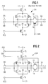
- FIG. 1 is a typical one Design of a sense amplifier according to the prior art shows.
- the known sense amplifier designated overall by LV1 1 contains a first pair of transistors consisting of two p-channel field effect transistors (P-FETs) T1 and T2, and a second transistor pair consisting of two n-channel field effect transistors (N-FETs) T3 and T4.
- the first main electrodes the P-FETs T1 and T2, in the case shown the source electrodes, are coupled together at a node 10, of the switching path of a first transistor switch T5 with a first power supply connection 11 is connected, which is the positive in the case shown Potential of a power supply source (not shown) receives.
- the source electrodes of the N-FETs T3 and T4 are on a node 20 coupled together via the Switching distance of a second transistor switch T6 with a second power supply connection 11 is connected, which in case shown the reference potential (e.g. ground potential) the power source receives.
- the first transistor switch T5 is a P-FET
- the second transistor switch T6 is an N-FET.
- the second main electrodes of transistors T1 and T3, in shown case, the drain electrodes, and the gate electrodes of transistors T2 and T4 are all with a first data connection BA connected to one of the two bit lines of a differential bit line pair, which is specifically assigned to the sense amplifier LV1. More like that Way are drain electrodes of transistors T2 and T4 and Gate electrodes of transistors T1 and T3 all with one second data connection BB connected to the other bit line of the differential couple.
- the two data connections BA and BB are also each via a gate switching transistor T7 and T8, respectively, in the case shown an N-FET, with a respectively assigned data line DA or DB connected in the illustrated embodiment a differential, bidirectional pair of data lines form.
- the four transistors T1 to T4 form a latch flip-flop, that with an effective power supply, so if the two transistors T5 and T5 are conductive, in one or other two stable (binary) states is triggerable to the binary information applied to the data connections BA and BB catch and hold as described below.
- each contains Row of the memory cell array two memory cells each per column position, one of which is the "true” binary value and the other stores the "complementary" binary value.
- Each of these two cells is associated with one Copy of the two bit lines of the column concerned associated bit line pair connected.
- With excitement one Word line will turn on the cell pairs of that row the respective bit line pairs coupled, so that between a potential difference between the two bit lines of the pair with a polarity representing the stored information arises. This potential difference appears at the data connections BA and BB of the pair assigned Sense amplifier.
- the sense amplifier LV1 becomes a shortly after excitation Word line turned on by the two transistor switches T5 and T6 by an assigned switch-on signal PES or NES can be made conductive.
- PES or NES switch-on signal
- the potential difference at the data connections such Polarity that BA is positive towards BB then the transistors T1 and T4 in the direction of increasing conductivity and transistors T3 and T3 increasing in the direction Blocking driven, so that BA on the positive supply potential of connection 11 and BB to that on connection 21 prevailing reference potential is drawn.
- the respective final state i.e. one or the other stable Binary state of the latch flip-flop T1-T4 is after the so-called "evaluation interval" reached, its length et al depends on the dimensioning of the sense amplifier LV1 and the shorter the higher its gain is. At the end this interval is sent to the sense amplifier if it is for one Write or read access should be selected
- Column selection signal SAS which is the gate switching transistors T7 and T8 makes conductive and thus that of the latch flip-flop T1-T4 "exploded" in the manner described Potential difference of the data connections BA, BB on the Data lines DA, DB couples.
- the information presented here can then on the data lines from a (not processing device shown) can be read.
- the sense amplifier according to the invention shown in FIG. 2 LV2 is the same as that of FIG. 1, with the only difference that an additional transistor switch T9 in one the power supply branches of the latch flip-flop is inserted. All other elements of the LV2 sense amplifier under construction and function of the elements of the sense amplifier shown in FIG. 1 LV1 correspond with the same reference numerals as described there and do not need to be described again become.
- the additional transistor switch is in the sense amplifier LV2 according to FIG. 2 T9 a P-FET, whose source-drain path (channel) in series with the transistor switch T5 between the positive Supply connection 11 and the coupled Source electrodes of the P-FETs T1, T2 of the latch flip-flop T1-T4 lies and the gate electrode of the column selection signal SAS receives, which also the gate switching transistors T7, T8 is created.
- the invention an additional support for preservation the potential difference to be read on the data lines DA, DB are provided.
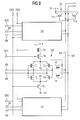
- This support can be an additional locking circuit (Latch) be. The effort for this is portable if a common data line for multiple sense amplifiers is used, which is usually the case. 3 shows an exemplary embodiment.
- a plurality of sense amplifiers is LV2 the design shown in Fig. 2 to a common data line pair DA, DB connected. Just one of those sense amplifiers LV2 is shown in detail, the others are through Blocks symbolize and have the same structure, and everyone is connected to its own bit line pair.
- the switch-on signals PES and NES are common to all sense amplifiers created. During a read or write cycle the individual sense amplifiers after excitation of a word line and applying the switch-on signals PES and NES, separately in different time slots through selectively created Column selection signals SAS driven for information successively in time over the common data line pair DA, DB read out or registered.
- a latch circuit is connected to the data line pair DA, DB, which contains two transistors T11 and T12 and practically half of the latch flip-flop of a sense amplifier LV2 replicates, namely that which by the invention Interruption of the power supply from one Fixed potential of the supply voltage is separated.
- the transistors T11 and T12 P-FETs the source electrodes of which are coupled together and associated with the positive potential of the supply source are similar to the transistors T1 and T2 of the latch flip-flop a sense amplifier LV2.
- the drain electrode of the transistor T11 and the gate electrode of transistor T12 are connected to the Data line DA connected while the drain electrode of Transistor T12 and the gate electrode of transistor T11 with the data line DB are connected. This connection corresponds the interconnection of transistors T1 and T2 with the Data connections BA and BB.
- the evaluation interval can run instead of the column selection signal SAS if requested a special, specially to interrupt control signal generated for this purpose is used become.
- the interruption according to the invention can be advantageous the power supply somewhat delayed compared to the Leading edge of the column selection signal SAS to begin, so that in the case of a reading operation, the information to be read is coupled to the data lines with greater power. This can be delayed by a special one Interrupt control signal or by response delay of the interruption switch T9 can be reached.
- the time of the beginning of the interruption should not be earlier than until the relevant latch flip-flop a the information content of the accessed memory cell indicating state, and that this At the latest in time in the active interval of the column selection signal in question falls to during this interval there is still enough time for a write operation to have.
- the for switching off the power supply of the sense amplifier Switching device used can also be arranged elsewhere than with transistor T9 in FIG. 2 or 3 is shown, e.g. as an interruption switch in the way of the supply line from the reference potential terminal 21 to the latch flip-flop T1-T4.
- transistors T11 and T12 would be the 3 form latch circuit 30 as N-FETs and with their source electrodes to the reference potential to join.
- the switching device can also be designed in this way or be arranged so that they are at least one of the existing Turn-on transistors T5, T6 blocks, for example using a suitable switching transistor in the control circuit of these transistors.
- the invention is neither based on the in the special design of the sense amplifier shown in the figures still on the use of paired bit and data lines is limited.
- single wire bit and data line paths has the latch flip-flop of the sense amplifier only a data connection, the potential of which is fixed Reference potential determines the binary state of the flip-flop or displays.
- the flip-flop can be made simpler be as shown in the figures.
- the invention can be used successfully with any type of "latching" sense amplifier be applied.
Landscapes
- Engineering & Computer Science (AREA)
- Microelectronics & Electronic Packaging (AREA)
- Computer Hardware Design (AREA)
- Static Random-Access Memory (AREA)
- Dram (AREA)
- Read Only Memory (AREA)
Abstract
Description
Claims (6)
- Schaltungsanordnung zum Lesen und Schreiben binärer Information an einem Speicherzellenfeld, das eine matrixförmige Anordnung aus Zeilen und Spalten von Speicherzellen bildet,
wobei der Zugriff auf eine beliebige Speicherzelle durch Erregung einer der betreffenden Zeile zugeordneten Wortleitung und durch Ansteuern einer der betreffenden Spalte zugeordneten Bitleitung über eine jeweils zugeordnete Schreib/Lese-Schaltung (LV2) erfolgt,
und wobei jede Schreib/Lese-Schaltung (LV2) ein Latch-Flipflop (T1-T4) mit mindestens einem Datenanschluß (BA, BB) enthält, der einerseits mit einer zugeordneten Bitleitung und andererseits über eine durch ein Spalten-Auswahlsignal (SAS) aufsteuerbare Torschaltung (T7, T8) mit einer Datenleitung (DA bzw. DB) verbunden ist,
gekennzeichnet durch
eine Schalteinrichtung (T9), die nach Erregung einer beliebigen Wortleitung die Stromversorgung der Latch-Flipflops (T1-T4) in den durch ein Spalten-Auswahlsignal (SAS) anzusteuernden Schreib/Lese-Schaltungen (LV2) ab einem Zeitpunkt unterbricht, der nicht früher ist, als bis das betreffende Latch-Flipflop einen den Informationsinhalt der zugegriffenen Speicherzelle anzeigenden Zustand eingenommen hat, und der spätestens in das aktive Intervall des betreffenden Spalten-Auswahlsignals fällt. - Schaltungsanordnung nach Anspruch 1, dadurch gekennzeichnet, dass die Schalteinrichtung einen Unterbrechungsschalter (T9) in jeder Schreib/Lese-Schaltung (LV2) enthält, der angeordnet ist zum Unterbrechen der Verbindung zwischen einem Versorgungspotential (+) und dem betreffenden Latch-Flipflop (T1-T4).
- Schaltungsanordnung nach Anspruch 2, dadurch gekennzeichnet, daß jeder Unterbrechungsschalter (T9) auf das Spalten-Auswahlsignal (SAS) der betreffenden Schreib/Lese-Schaltung (LV2) anspricht, um die Unterbrechung der Stromversorgung mit Beginn dieses Spalten-Auswahlsignals einzuleiten und für die Dauer des Spalten-Auswahlsignals aufrechtzuerhalten.
- Schaltungsanordnung nach Anspruch 2 oder 3, in welcher jedes Latch-Flipflop (T1-T4) ein erstes Transistorpaar (T1, T2) enthält, bei dem die Steuerelektrode jedes Transistors mit einer Hauptelektrode des jeweils anderen Transistors verbunden ist und die Steuerelektrode eines der Transistoren (T1 bzw. T2) mit einem Datenanschluß (BB bzw. BA) des Latch-Flipflops verbunden ist und die anderen Hauptelektroden der beiden Transistoren mit einem Schaltungspunkt (10) zum Empfang eines ersten Versorgungspotentials (+) verbunden sind, dadurch gekennzeichnet, daß der Unterbrechungsschalter (T9) zwischen dem genannten Schaltungspunkt (10) und einem das erste Versorgungspotential (+) empfangenden Versorgungsanschluß (11) der betreffenden Schreib/Lese-Schaltung (LV2) angeordnet ist.
- Schaltungsanordnung nach einem der Ansprüche 1 bis 4, in welcher die Datenleitung (DA bzw. DB) mehreren Schreib/Lese-Schaltungen (LV2) gemeinsam ist, dadurch gekennzeichnet, daß mit der Datenleitung (DA bzw. DB) eine Verriegelungsschaltung (30) verbunden ist, die den Binärzustand des Datenanschlusses (BA bzw. BB) eines Latch-Flipflops (T1-T4), der von der zugeordneten Torschaltung auf die Datenleitung gekoppelt wird, an der Datenleitung verriegelt.
- Schaltungsanordnung nach den Ansprüchen 4 oder 5, dadurch gekennzeichnet, daß die Verriegelungsschaltung (30) ein Transistorpaar (T11, T12) aufweist, das hinsichtlich des Leitungstyps dem ersten Transistorpaar (T1, T2) gleicht und bei dem die Steuerelektrode jedes Transistors mit einer Hauptelektrode des jeweils anderen Transistors verbunden ist und die Steuerelektrode eines der Transistoren mit der genannten gemeinsamen Datenleitung verbunden ist und die anderen Hauptelektroden der beiden Transistoren mit einem das erste Versorgungspotential (+) empfangenden Versorgungsanschluß (31) verbunden sind.
Applications Claiming Priority (2)
| Application Number | Priority Date | Filing Date | Title |
|---|---|---|---|
| DE10034255 | 2000-07-14 | ||
| DE10034255A DE10034255C2 (de) | 2000-07-14 | 2000-07-14 | Schaltungsanordnung zum Lesen und Schreiben von Information an einem Speicherzellenfeld |
Publications (1)
| Publication Number | Publication Date |
|---|---|
| EP1172819A1 true EP1172819A1 (de) | 2002-01-16 |
Family
ID=7648911
Family Applications (1)
| Application Number | Title | Priority Date | Filing Date |
|---|---|---|---|
| EP01113285A Withdrawn EP1172819A1 (de) | 2000-07-14 | 2001-05-31 | Schaltungsanordnung zum Lesen und Schreiben von Information an einem Speicherzellenfeld |
Country Status (4)
| Country | Link |
|---|---|
| US (1) | US6487127B2 (de) |
| EP (1) | EP1172819A1 (de) |
| DE (1) | DE10034255C2 (de) |
| TW (1) | TW514934B (de) |
Families Citing this family (5)
| Publication number | Priority date | Publication date | Assignee | Title |
|---|---|---|---|---|
| US6989861B2 (en) * | 2001-09-14 | 2006-01-24 | Hewlett-Packard Development Company, L.P. | User selection of power-on configuration |
| DE10323863B4 (de) * | 2003-05-26 | 2005-09-22 | Infineon Technologies Ag | Integrierte Schaltung und Verfahren zum Betreiben einer integrierten Schaltung |
| TWI286764B (en) * | 2005-01-20 | 2007-09-11 | Himax Tech Ltd | Memory architecture of display device and memory writing method for the same |
| US20120281459A1 (en) * | 2011-05-08 | 2012-11-08 | Ben-Gurion University Of The Negev Research And Development Authority | Ultra low power memory cell with a supply feedback loop configured for minimal leakage operation |
| US8531873B2 (en) | 2011-05-08 | 2013-09-10 | Ben-Gurion University Of The Negev Research And Development Authority | Ultra low power SRAM cell circuit with a supply feedback loop for near and sub threshold operation |
Citations (2)
| Publication number | Priority date | Publication date | Assignee | Title |
|---|---|---|---|---|
| WO1985002314A2 (en) * | 1983-12-02 | 1985-06-06 | American Telephone & Telegraph Company | Semiconductor memory |
| US5291447A (en) * | 1991-07-30 | 1994-03-01 | Fujitsu Limited | Semiconductor memory device having function of controlling sense amplifiers |
Family Cites Families (9)
| Publication number | Priority date | Publication date | Assignee | Title |
|---|---|---|---|---|
| JPS6032911B2 (ja) * | 1979-07-26 | 1985-07-31 | 株式会社東芝 | 半導体記憶装置 |
| JPH0438793A (ja) * | 1990-06-04 | 1992-02-07 | Toshiba Corp | データ転送制御回路およびこれを用いたダイナミック型半導体記憶装置 |
| JPH0696582A (ja) * | 1990-09-17 | 1994-04-08 | Texas Instr Inc <Ti> | メモリアレイアーキテクチャ |
| JPH087573A (ja) * | 1994-06-14 | 1996-01-12 | Mitsubishi Electric Corp | 半導体記憶装置と、そのデータの読出および書込方法 |
| US5764580A (en) * | 1995-08-18 | 1998-06-09 | Hitachi, Ltd. | Semiconductor integrated circuit |
| TW348266B (en) * | 1996-03-11 | 1998-12-21 | Toshiba Co Ltd | Semiconductor memory device |
| US5877987A (en) * | 1997-02-14 | 1999-03-02 | Micron Technology, Inc. | Method and circuit for self-latching data read lines in the data output path of a semiconductor memory device |
| US5862089A (en) * | 1997-08-14 | 1999-01-19 | Micron Technology, Inc. | Method and memory device for dynamic cell plate sensing with ac equilibrate |
| JP3971032B2 (ja) * | 1997-12-10 | 2007-09-05 | 富士通株式会社 | 半導体記憶装置、半導体記憶装置のデータ読み出し方法、及びデータ記憶装置 |
-
2000
- 2000-07-14 DE DE10034255A patent/DE10034255C2/de not_active Expired - Fee Related
-
2001
- 2001-05-31 EP EP01113285A patent/EP1172819A1/de not_active Withdrawn
- 2001-07-12 TW TW090117070A patent/TW514934B/zh not_active IP Right Cessation
- 2001-07-16 US US09/906,451 patent/US6487127B2/en not_active Expired - Fee Related
Patent Citations (2)
| Publication number | Priority date | Publication date | Assignee | Title |
|---|---|---|---|---|
| WO1985002314A2 (en) * | 1983-12-02 | 1985-06-06 | American Telephone & Telegraph Company | Semiconductor memory |
| US5291447A (en) * | 1991-07-30 | 1994-03-01 | Fujitsu Limited | Semiconductor memory device having function of controlling sense amplifiers |
Also Published As
| Publication number | Publication date |
|---|---|
| DE10034255A1 (de) | 2002-01-31 |
| DE10034255C2 (de) | 2002-05-16 |
| US6487127B2 (en) | 2002-11-26 |
| TW514934B (en) | 2002-12-21 |
| US20020015331A1 (en) | 2002-02-07 |
Similar Documents
| Publication | Publication Date | Title |
|---|---|---|
| DE3751171T2 (de) | Ferro-elektrischer Speicher mit automatischer Wiederherstellung. | |
| DE2932019C2 (de) | Speicheranordnung | |
| DE3887130T2 (de) | Ferro-elektrisches Festhalteverfahren. | |
| DE2556831C2 (de) | Matrixspeicher und Verfahren zu seinem Betrieb | |
| DE2659248B2 (de) | ||
| DE2650479C2 (de) | Speicheranordnung mit Ladungsspeicherzellen | |
| DE3802363A1 (de) | Halbleiterspeicher | |
| EP0012796B1 (de) | Speicheranordnung mit Speicherzellen zum gleichzeitigen Einlesen und Auslesen von Information | |
| DE2525225A1 (de) | Schaltungsanordnung zur anzeige der verschiebung elektrischer ladung | |
| DE2721851A1 (de) | Verriegelnder leseverstaerker fuer halbleiterspeicheranordnungen | |
| DE60202312T2 (de) | Speicherzelle, nichtflüchtige Speicheranordnung und Steuerungsverfahren dafür, Zulässigkeitsverbesserung bei niedriger Speisespannung | |
| DE2413804C2 (de) | Schaltungsanordnung für eine wortorganisierte Halbleiterspeichermatrix | |
| DE1774401A1 (de) | Optischer Speicher mit photoaktivem Speicherelement | |
| DE3101520A1 (de) | Monolithisch integrierter halbleiterspeicher | |
| DE1279747B (de) | Speicherzelle | |
| DE10034255C2 (de) | Schaltungsanordnung zum Lesen und Schreiben von Information an einem Speicherzellenfeld | |
| DE1524900A1 (de) | Bistabile Schaltungsanordnung mit zwei Transistoren | |
| DE1186509B (de) | Magnetspeicher mit einem mit zueinander senkrechten Bohrungen versehenen Magnetkern | |
| DE2359153A1 (de) | Integrierte treiberschaltung zur anwendung in einem halbleiterspeicher | |
| DE68925181T2 (de) | Digitales Speichersystem | |
| DE68927255T2 (de) | Impulsgeneratorschaltung | |
| DE69720126T2 (de) | Wortleitungstreiberschaltung für Flash-EEPROM-Speicher | |
| DE2152706B2 (de) | Monolithischer integrierter halbleiterspeicher fuer binaere daten | |
| DE2618760C3 (de) | Halbleiter-Speichervorrichtung | |
| DE60224406T2 (de) | Direktzugriffspeicheranordnungen mit einem diodenpuffer |
Legal Events
| Date | Code | Title | Description |
|---|---|---|---|
| PUAI | Public reference made under article 153(3) epc to a published international application that has entered the european phase |
Free format text: ORIGINAL CODE: 0009012 |
|
| AK | Designated contracting states |
Kind code of ref document: A1 Designated state(s): AT BE CH CY DE DK ES FI FR GB GR IE IT LI LU MC NL PT SE TR Kind code of ref document: A1 Designated state(s): DE GB IE |
|
| AX | Request for extension of the european patent |
Free format text: AL;LT;LV;MK;RO;SI |
|
| 17P | Request for examination filed |
Effective date: 20020703 |
|
| AKX | Designation fees paid |
Free format text: DE GB IE |
|
| 17Q | First examination report despatched |
Effective date: 20071105 |
|
| STAA | Information on the status of an ep patent application or granted ep patent |
Free format text: STATUS: THE APPLICATION IS DEEMED TO BE WITHDRAWN |
|
| 18D | Application deemed to be withdrawn |
Effective date: 20080724 |