EP1161128A1 - Abgeschirmte, elektronische Schaltung - Google Patents
Abgeschirmte, elektronische Schaltung Download PDFInfo
- Publication number
- EP1161128A1 EP1161128A1 EP01108577A EP01108577A EP1161128A1 EP 1161128 A1 EP1161128 A1 EP 1161128A1 EP 01108577 A EP01108577 A EP 01108577A EP 01108577 A EP01108577 A EP 01108577A EP 1161128 A1 EP1161128 A1 EP 1161128A1
- Authority
- EP
- European Patent Office
- Prior art keywords
- shield
- outer shield
- electronic circuit
- circuit according
- inner shield
- Prior art date
- Legal status (The legal status is an assumption and is not a legal conclusion. Google has not performed a legal analysis and makes no representation as to the accuracy of the status listed.)
- Granted
Links
Images
Classifications
-
- H—ELECTRICITY
- H05—ELECTRIC TECHNIQUES NOT OTHERWISE PROVIDED FOR
- H05K—PRINTED CIRCUITS; CASINGS OR CONSTRUCTIONAL DETAILS OF ELECTRIC APPARATUS; MANUFACTURE OF ASSEMBLAGES OF ELECTRICAL COMPONENTS
- H05K9/00—Screening of apparatus or components against electric or magnetic fields
- H05K9/0007—Casings
- H05K9/002—Casings with localised screening
- H05K9/0022—Casings with localised screening of components mounted on printed circuit boards [PCB]
- H05K9/0024—Shield cases mounted on a PCB, e.g. cans or caps or conformal shields
-
- H—ELECTRICITY
- H05—ELECTRIC TECHNIQUES NOT OTHERWISE PROVIDED FOR
- H05K—PRINTED CIRCUITS; CASINGS OR CONSTRUCTIONAL DETAILS OF ELECTRIC APPARATUS; MANUFACTURE OF ASSEMBLAGES OF ELECTRICAL COMPONENTS
- H05K9/00—Screening of apparatus or components against electric or magnetic fields
- H05K9/0007—Casings
- H05K9/002—Casings with localised screening
- H05K9/0022—Casings with localised screening of components mounted on printed circuit boards [PCB]
- H05K9/0024—Shield cases mounted on a PCB, e.g. cans or caps or conformal shields
- H05K9/0032—Shield cases mounted on a PCB, e.g. cans or caps or conformal shields having multiple parts, e.g. frames mating with lids
-
- Y—GENERAL TAGGING OF NEW TECHNOLOGICAL DEVELOPMENTS; GENERAL TAGGING OF CROSS-SECTIONAL TECHNOLOGIES SPANNING OVER SEVERAL SECTIONS OF THE IPC; TECHNICAL SUBJECTS COVERED BY FORMER USPC CROSS-REFERENCE ART COLLECTIONS [XRACs] AND DIGESTS
- Y10—TECHNICAL SUBJECTS COVERED BY FORMER USPC
- Y10S—TECHNICAL SUBJECTS COVERED BY FORMER USPC CROSS-REFERENCE ART COLLECTIONS [XRACs] AND DIGESTS
- Y10S174/00—Electricity: conductors and insulators
- Y10S174/35—Box or housing mounted on substrate or PCB
Definitions
- the invention relates to one with an outer shield provided electronic circuit, which within the outer shield to protect against each other Influencing electronic components at least one has inner shielding.
- Electronic circuits of the above type are in well known and common in the art, for example in motor vehicles for vehicle navigation devices.
- the shields serve the electronic Components before electromagnetic interference from protect outside and a radiation of electromagnetic Prevent waves outward so the circuit do not interfere with other electronic devices can.
- the shields for example, a thermal rubber however, requires a relatively high installation effort and requires tight tolerances of the components, so not too very different distances between the two Shields must be bridged. Furthermore, the Heat conduction is often insufficient because the heat initially from one shield into the thermal rubber and then from the thermal rubber to the other Shield must pass before the outer shield can give off the heat to the ambient air.
- the invention is based on the problem of a shielded electronic circuit of the aforementioned Kind of like that in the inner shield incoming heat can be optimally dissipated to the outside can without the circuit therefore with high accuracy must be manufactured and assembled.
- This design becomes the real cause of the problem of poor cooling of the inner shield, namely the separation of the electronic component eliminated within the inner shield by two walls.
- the gaps between the two shields must be with Consideration of the wavelengths of the interfering frequencies be measured. This is difficult because it is not can be clearly predicted with which areas the outer shield rests on the inner shield. Such uncertainties can be avoided if the outer shield along the edge of the opening with indentations on the inside Shield rests and the spacing of the indentations tuned to the wavelength of the interfering frequencies are.
- the spring tongues are particularly capable of large differences in distance to compensate if according to another training the invention the spring tongues to compensate different heights of the shields Z-shaped run curved.
- the smallest possible construction volume results if the inner shield has a greater height than the outer Shield and the z-shaped tongues of the outer shield from the level of the outer shield to the level the inner shield.
- the electronic circuit is optimally designed as a whole, if the outer shield on a main circuit board attached, which is inside the outer Shield one at a distance from the main circuit board parallel daughter board with at least another electronic component and if the inner shield attached to this daughter board is.
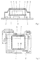
- Figure 1 shows a main circuit board 1, on the various electronic components 2, 3, 4 arranged are. At a distance and parallel to the main circuit board 1 is on it a daughter board 5 with an electronic Component 6 attached. This electronic component 6 is encapsulated by an inner shield 7. The entire electronic circuit is from an external Shield 8 covered. This has an opening 9, limited by the z-shaped spring tongues 10 which is each a spherical dome-shaped indentation 11, which with bias from above the inner shield 7 rests.
- FIG. 2 shows the main circuit board 1 with the one on it arranged outer shield 8. Furthermore one recognizes the opening 9, which is limited by the spring tongues 10 is, each with their indentation 11 on the inner shield 7 rests with pretension.
Landscapes
- Engineering & Computer Science (AREA)
- Microelectronics & Electronic Packaging (AREA)
- Shielding Devices Or Components To Electric Or Magnetic Fields (AREA)
Abstract
Description
- Fig.1
- einen Schnitt durch eine elektronische Schaltung nach der Erfindung,
- Fig.2
- eine Draufsicht auf eine erfindungsgemäße elektronische Schaltung.
Claims (7)
- Mit einer äußeren Abschirmung versehene elektronische Schaltung, welche innerhalb der äußeren Abschirmung zum Schutz vor einer gegenseitigen Beeinflussung elektronischer Bauteile zumindest eine innere Abschirmung aufweist, dadurch gekennzeichnet, dass die äußere Abschirmung (8) auf der inneren Abschirmung (7) aufliegt und im Bereich der inneren Abschirmung (7) eine Durchbrechung (9) hat.
- Elektronische Schaltung nach Anspruch 1, dadurch gekennzeichnet, dass die Durchbrechung (9) der äußeren Abschirmung (8) durch eine Vielzahl nebeneinander angeordneter Federzungen (10) begrenzt ist, welche auf der inneren Abschirmung (7) mit Vorspannung aufliegen.
- Elektronische Schaltung nach den Ansprüchen 1 oder 2, dadurch gekennzeichnet, dass die äußere Abschirmung (8) entlang des Randes der Durchbrechung (9) mit kugelkalottenförmigen Eindrückungen (11) auf der inneren Abschirmung (7) aufliegt und die Abstände der Eindrückungen (11) auf die Wellenlänge der störenden Frequenzen abgestimmt sind.
- Elektronische Schaltung nach Anspruch 3, dadurch gekennzeichnet, dass die Eindrückungen (11) in den Federzungen (10) vorgesehen sind.
- Elektronische Schaltung nach zumindest einem der vorangehenden Ansprüche, dadurch gekennzeichnet, dass die Federzungen (10) zum Ausgleich unterschiedlicher Höhenlagen der Abschirmungen (7, 8) z-förmig gebogen verlaufen.
- Elektronische Schaltung nach zumindest einem der vorangehenden Ansprüche, dadurch gekennzeichnet, dass die innere Abschirmung (7) eine größere Höhe hat als die äußere Abschirmung (8) und die z-förmigen Zungen (10) der äußeren Abschirmung (8) aus der Ebene der äußeren Abschirmung (8) zur Ebene der inneren Abschirmung (7) hochgeführt sind.
- Elektronische Schaltung nach zumindest einem der vorangehenden Ansprüche, dadurch gekennzeichnet, dass die äußere Abschirmung (8) auf einer Hauptleiterplatte (1) befestigt ist, welche innerhalb der äußeren Abschirmung (8) eine mit Abstand zu der Hauptleiterplatte (1) parallel verlaufende Tochterleiterplatte (5) mit zumindest einem weiteren, elektronischen Bauteil (6) trägt und dass die innere Abschirmung (7) auf dieser Tochterleiterplatte (5) befestigt ist.
Applications Claiming Priority (2)
| Application Number | Priority Date | Filing Date | Title |
|---|---|---|---|
| DE10026353A DE10026353A1 (de) | 2000-05-27 | 2000-05-27 | Abgeschirmte, elektronische Schaltung |
| DE10026353 | 2000-05-27 |
Publications (2)
| Publication Number | Publication Date |
|---|---|
| EP1161128A1 true EP1161128A1 (de) | 2001-12-05 |
| EP1161128B1 EP1161128B1 (de) | 2003-11-12 |
Family
ID=7643806
Family Applications (1)
| Application Number | Title | Priority Date | Filing Date |
|---|---|---|---|
| EP01108577A Expired - Lifetime EP1161128B1 (de) | 2000-05-27 | 2001-04-05 | Abgeschirmte, elektronische Schaltung |
Country Status (4)
| Country | Link |
|---|---|
| US (1) | US6590783B2 (de) |
| EP (1) | EP1161128B1 (de) |
| JP (1) | JP2001339194A (de) |
| DE (2) | DE10026353A1 (de) |
Cited By (1)
| Publication number | Priority date | Publication date | Assignee | Title |
|---|---|---|---|---|
| EP2391028A3 (de) * | 2010-05-25 | 2014-08-20 | BlackBerry Limited | Mobile drahtlose Kommunikationsvorrichtung mit HF-Abschirmung und zugehörige Verfahren |
Families Citing this family (30)
| Publication number | Priority date | Publication date | Assignee | Title |
|---|---|---|---|---|
| WO2004077898A2 (en) * | 2003-02-26 | 2004-09-10 | Wavezero Inc. | Methods and devices for connecting and grounding an emi shield to a printed circuit board |
| JP2004296859A (ja) * | 2003-03-27 | 2004-10-21 | Renesas Technology Corp | 磁気記録素子及び磁気記録素子の製造方法 |
| JP4037810B2 (ja) * | 2003-09-05 | 2008-01-23 | Necアクセステクニカ株式会社 | 小型無線装置及びその実装方法 |
| JP4052995B2 (ja) * | 2003-10-27 | 2008-02-27 | 三洋電機株式会社 | 回路装置 |
| JP2005268428A (ja) * | 2004-03-17 | 2005-09-29 | Mitsubishi Electric Corp | 基板の電磁シールド構造 |
| JP4555119B2 (ja) * | 2005-02-22 | 2010-09-29 | アルプス電気株式会社 | 面実装型電子回路ユニット |
| KR101103967B1 (ko) | 2005-08-29 | 2012-01-06 | 엘지이노텍 주식회사 | 실드 캔 실장용 지그 장치 |
| US7262369B1 (en) | 2006-03-09 | 2007-08-28 | Laird Technologies, Inc. | Combined board level EMI shielding and thermal management |
| KR100724916B1 (ko) * | 2006-01-02 | 2007-06-04 | 삼성전자주식회사 | 전자회로 패키지 |
| US7623360B2 (en) * | 2006-03-09 | 2009-11-24 | Laird Technologies, Inc. | EMI shielding and thermal management assemblies including frames and covers with multi-position latching |
| US7317618B2 (en) * | 2006-03-09 | 2008-01-08 | Laird Technologies, Inc. | Combined board level shielding and thermal management |
| US7463496B2 (en) * | 2006-03-09 | 2008-12-09 | Laird Technologies, Inc. | Low-profile board level EMI shielding and thermal management apparatus and spring clips for use therewith |
| CN101595771B (zh) * | 2007-01-29 | 2011-09-14 | 日本电气株式会社 | 电子装置的屏蔽结构以及包括屏蔽结构的电子装置 |
| TWM318903U (en) * | 2007-04-03 | 2007-09-11 | Chin-Fu Horng | Electromagnetic shielding device |
| CN101453826B (zh) * | 2007-11-28 | 2011-12-21 | 深圳富泰宏精密工业有限公司 | 印刷电路板堆叠结构 |
| US8134846B2 (en) * | 2009-05-08 | 2012-03-13 | Utc Fire & Security Americas Corporation, Inc. | Apparatus for shielding H-field signals |
| US8477499B2 (en) | 2009-06-05 | 2013-07-02 | Laird Technologies, Inc. | Assemblies and methods for dissipating heat from handheld electronic devices |
| US7965514B2 (en) | 2009-06-05 | 2011-06-21 | Laird Technologies, Inc. | Assemblies and methods for dissipating heat from handheld electronic devices |
| JP5407846B2 (ja) * | 2009-12-25 | 2014-02-05 | 株式会社Jvcケンウッド | 基板の取付構造及び電子機器 |
| US8169781B2 (en) * | 2010-04-06 | 2012-05-01 | Fsp Technology Inc. | Power supply and heat dissipation module thereof |
| US8681493B2 (en) * | 2011-05-10 | 2014-03-25 | Kla-Tencor Corporation | Heat shield module for substrate-like metrology device |
| US9048124B2 (en) * | 2012-09-20 | 2015-06-02 | Apple Inc. | Heat sinking and electromagnetic shielding structures |
| KR102553474B1 (ko) * | 2016-04-20 | 2023-07-10 | 에이치엘만도 주식회사 | 방열 및 센싱구조가 향상된 전자제어유닛 |
| CN106061213B (zh) * | 2016-08-05 | 2018-02-09 | 深圳市众易畅科技有限公司 | 汽车内装人机互动显示屏集成散热系统及散热方法 |
| JP2018064042A (ja) * | 2016-10-13 | 2018-04-19 | イビデン株式会社 | シールドキャップ及びその製造方法 |
| JP2018064043A (ja) * | 2016-10-13 | 2018-04-19 | イビデン株式会社 | シールドキャップ及びその製造方法 |
| JP6947071B2 (ja) * | 2018-02-13 | 2021-10-13 | 株式会社オートネットワーク技術研究所 | インダクタ、基板付きインダクタ及び電気接続箱 |
| JP7253048B2 (ja) * | 2019-05-23 | 2023-04-05 | 株式会社ソニー・インタラクティブエンタテインメント | 電子機器 |
| CN110430739A (zh) * | 2019-06-27 | 2019-11-08 | 芜湖宏景电子股份有限公司 | 一种车载cpu核心散热屏蔽结构 |
| JP2021064670A (ja) * | 2019-10-11 | 2021-04-22 | 株式会社デンソー | 電子機器 |
Citations (4)
| Publication number | Priority date | Publication date | Assignee | Title |
|---|---|---|---|---|
| EP0519767A2 (de) * | 1991-09-19 | 1992-12-23 | Nokia Mobile Phones Ltd. | Eine Leiterplattenanordnung |
| EP0632686A1 (de) * | 1993-06-29 | 1995-01-04 | Telefonaktiebolaget Lm Ericsson | Vorrichtung zur Schirmung und/oder Kühlung den elektronischen Komponenten |
| JPH1041678A (ja) * | 1996-07-25 | 1998-02-13 | Hitachi Ltd | 光受信器 |
| EP0926940A1 (de) * | 1997-12-11 | 1999-06-30 | Intermec Ip Corp. | Verfahren und Vorrichtung zur elektromagnetischen Abschirmung in einer PCMCIA Flachbaugruppe |
Family Cites Families (9)
| Publication number | Priority date | Publication date | Assignee | Title |
|---|---|---|---|---|
| JPH036099A (ja) * | 1989-06-02 | 1991-01-11 | Canon Inc | 電子機器の実装構造 |
| US5354951A (en) * | 1993-03-15 | 1994-10-11 | Leader Tech, Inc. | Circuit board component shielding enclosure and assembly |
| US5761053A (en) * | 1996-05-08 | 1998-06-02 | W. L. Gore & Associates, Inc. | Faraday cage |
| JPH11307974A (ja) * | 1998-04-27 | 1999-11-05 | Sony Corp | 電磁波シールド装置と電磁波シールド方法 |
| DE19921692B4 (de) * | 1998-11-24 | 2008-12-11 | Continental Teves Ag & Co. Ohg | Anordnung zum Schutz von elektronischen Funktionseinheiten und/oder Funktionsgruppen |
| JP2000307289A (ja) * | 1999-04-19 | 2000-11-02 | Nec Corp | 電子部品組立体 |
| US6269008B1 (en) * | 1999-11-22 | 2001-07-31 | Lucent Technologies Inc. | Multi-walled electromagnetic interference shield |
| TW477516U (en) * | 2000-04-18 | 2002-02-21 | Hon Hai Prec Ind Co Ltd | Shielding structure of electronic device |
| US6490173B2 (en) * | 2000-12-19 | 2002-12-03 | Thomson Licensing, S.A. | Method and apparatus for providing electromagnetic shielding |
-
2000
- 2000-05-27 DE DE10026353A patent/DE10026353A1/de not_active Withdrawn
-
2001
- 2001-04-05 EP EP01108577A patent/EP1161128B1/de not_active Expired - Lifetime
- 2001-04-05 DE DE50100936T patent/DE50100936D1/de not_active Expired - Fee Related
- 2001-05-24 JP JP2001155956A patent/JP2001339194A/ja not_active Withdrawn
- 2001-05-24 US US09/864,690 patent/US6590783B2/en not_active Expired - Fee Related
Patent Citations (4)
| Publication number | Priority date | Publication date | Assignee | Title |
|---|---|---|---|---|
| EP0519767A2 (de) * | 1991-09-19 | 1992-12-23 | Nokia Mobile Phones Ltd. | Eine Leiterplattenanordnung |
| EP0632686A1 (de) * | 1993-06-29 | 1995-01-04 | Telefonaktiebolaget Lm Ericsson | Vorrichtung zur Schirmung und/oder Kühlung den elektronischen Komponenten |
| JPH1041678A (ja) * | 1996-07-25 | 1998-02-13 | Hitachi Ltd | 光受信器 |
| EP0926940A1 (de) * | 1997-12-11 | 1999-06-30 | Intermec Ip Corp. | Verfahren und Vorrichtung zur elektromagnetischen Abschirmung in einer PCMCIA Flachbaugruppe |
Non-Patent Citations (1)
| Title |
|---|
| PATENT ABSTRACTS OF JAPAN vol. 1998, no. 06 30 April 1998 (1998-04-30) * |
Cited By (2)
| Publication number | Priority date | Publication date | Assignee | Title |
|---|---|---|---|---|
| EP2391028A3 (de) * | 2010-05-25 | 2014-08-20 | BlackBerry Limited | Mobile drahtlose Kommunikationsvorrichtung mit HF-Abschirmung und zugehörige Verfahren |
| US9036367B2 (en) | 2010-05-25 | 2015-05-19 | Blackberry Limited | Mobile wireless communications device with RF shield and related methods |
Also Published As
| Publication number | Publication date |
|---|---|
| US20020003695A1 (en) | 2002-01-10 |
| DE50100936D1 (de) | 2003-12-18 |
| DE10026353A1 (de) | 2001-11-29 |
| US6590783B2 (en) | 2003-07-08 |
| EP1161128B1 (de) | 2003-11-12 |
| JP2001339194A (ja) | 2001-12-07 |
Similar Documents
| Publication | Publication Date | Title |
|---|---|---|
| EP1161128B1 (de) | Abgeschirmte, elektronische Schaltung | |
| DE69504471T2 (de) | Vorrichtung zur Verhinderung elektromagnetischer Störung | |
| EP0575436B1 (de) | Vorrichtung zur kontaktierung von wanne und haube eines geschlossenen gehäuses | |
| DE3527267A1 (de) | Elektromagnetische abschirmung | |
| DE3445161C2 (de) | ||
| DE69817220T2 (de) | Oberflächenmontierter federkontaktstreifen und emi gehause | |
| DE69737447T2 (de) | Elektronische Karte mit Abschirmabdeckung, die Laschen beinhaltet, wobei jede dieser Laschen in eine Aussparung der korrespondierenden Abschirmabdeckung eingreift | |
| DE69001420T2 (de) | Modulgehaeuse fuer zwei inkompatible schaltkreise. | |
| DE102017129402A1 (de) | Leiterplattengehäuse mit führungsrippen | |
| DE60104738T2 (de) | Hochfrequenz-Kommunikationsgerät und Verfahren zu dessen Herstellung | |
| DE102012213520A1 (de) | Gehäuse für eine Leiterplatte und Elektrogerät | |
| EP0756447B1 (de) | Schaltungsanordnung für Kraftfahrzeuge | |
| EP0941644A1 (de) | Elektronischer schaltkreis mit einem hockfrequenzbedämpfenden schirmgehäuse | |
| DE10149305C1 (de) | Abschirmelement zur elektromagnetischen Abschirmung einer Durchgangsöffnung | |
| DE69003727T2 (de) | Mobiles Miniatur-Funkgerät mit Abschirmungsanordnung. | |
| DE69208426T2 (de) | Baugruppenträger | |
| DE19649433C2 (de) | Anordnung zur Abschirmung gegen elektromagnetische Kopplung | |
| DE69824984T2 (de) | Schutzgehäuse für eine Leiterplatte | |
| DE3915651C2 (de) | ||
| DE9103080U1 (de) | Abgeschirmtes Gehäuse für elektrische Geräte | |
| DE69803593T2 (de) | Gerät | |
| DE3440739C2 (de) | ||
| DE3413533A1 (de) | Elektrotechnisches geraet, insbesondere fuer die nachrichtentechnik | |
| DE9400526U1 (de) | Knickbare HF-dichte Abschirmwand für gedruckte Schaltungen | |
| DE3629913A1 (de) | Abschirmgehaeuse |
Legal Events
| Date | Code | Title | Description |
|---|---|---|---|
| PUAI | Public reference made under article 153(3) epc to a published international application that has entered the european phase |
Free format text: ORIGINAL CODE: 0009012 |
|
| AK | Designated contracting states |
Kind code of ref document: A1 Designated state(s): AT BE CH CY DE DK ES FI FR GB GR IE IT LI LU MC NL PT SE TR Kind code of ref document: A1 Designated state(s): DE FR GB |
|
| AX | Request for extension of the european patent |
Free format text: AL;LT;LV;MK;RO;SI |
|
| RAP1 | Party data changed (applicant data changed or rights of an application transferred) |
Owner name: SIEMENS AKTIENGESELLSCHAFT |
|
| 17P | Request for examination filed |
Effective date: 20020121 |
|
| AKX | Designation fees paid |
Free format text: DE FR GB |
|
| GRAH | Despatch of communication of intention to grant a patent |
Free format text: ORIGINAL CODE: EPIDOS IGRA |
|
| GRAH | Despatch of communication of intention to grant a patent |
Free format text: ORIGINAL CODE: EPIDOS IGRA |
|
| GRAA | (expected) grant |
Free format text: ORIGINAL CODE: 0009210 |
|
| AK | Designated contracting states |
Kind code of ref document: B1 Designated state(s): DE FR GB |
|
| REG | Reference to a national code |
Ref country code: GB Ref legal event code: FG4D Free format text: NOT ENGLISH |
|
| REF | Corresponds to: |
Ref document number: 50100936 Country of ref document: DE Date of ref document: 20031218 Kind code of ref document: P |
|
| REG | Reference to a national code |
Ref country code: IE Ref legal event code: FG4D Free format text: GERMAN |
|
| GBT | Gb: translation of ep patent filed (gb section 77(6)(a)/1977) |
Effective date: 20040130 |
|
| REG | Reference to a national code |
Ref country code: IE Ref legal event code: FD4D |
|
| ET | Fr: translation filed | ||
| PLBE | No opposition filed within time limit |
Free format text: ORIGINAL CODE: 0009261 |
|
| STAA | Information on the status of an ep patent application or granted ep patent |
Free format text: STATUS: NO OPPOSITION FILED WITHIN TIME LIMIT |
|
| 26N | No opposition filed |
Effective date: 20040813 |
|
| PGFP | Annual fee paid to national office [announced via postgrant information from national office to epo] |
Ref country code: GB Payment date: 20080417 Year of fee payment: 8 |
|
| PGFP | Annual fee paid to national office [announced via postgrant information from national office to epo] |
Ref country code: DE Payment date: 20090422 Year of fee payment: 9 |
|
| GBPC | Gb: european patent ceased through non-payment of renewal fee |
Effective date: 20090405 |
|
| REG | Reference to a national code |
Ref country code: FR Ref legal event code: ST Effective date: 20091231 |
|
| PG25 | Lapsed in a contracting state [announced via postgrant information from national office to epo] |
Ref country code: FR Free format text: LAPSE BECAUSE OF NON-PAYMENT OF DUE FEES Effective date: 20091222 Ref country code: GB Free format text: LAPSE BECAUSE OF NON-PAYMENT OF DUE FEES Effective date: 20090405 |
|
| PGFP | Annual fee paid to national office [announced via postgrant information from national office to epo] |
Ref country code: FR Payment date: 20080422 Year of fee payment: 8 |
|
| PG25 | Lapsed in a contracting state [announced via postgrant information from national office to epo] |
Ref country code: DE Free format text: LAPSE BECAUSE OF NON-PAYMENT OF DUE FEES Effective date: 20101103 |