EP1158533B1 - EEPROM-Matrix mit einem, dem "Flash"-Speicher ähnlichen Kern - Google Patents
EEPROM-Matrix mit einem, dem "Flash"-Speicher ähnlichen Kern Download PDFInfo
- Publication number
- EP1158533B1 EP1158533B1 EP01117713A EP01117713A EP1158533B1 EP 1158533 B1 EP1158533 B1 EP 1158533B1 EP 01117713 A EP01117713 A EP 01117713A EP 01117713 A EP01117713 A EP 01117713A EP 1158533 B1 EP1158533 B1 EP 1158533B1
- Authority
- EP
- European Patent Office
- Prior art keywords
- memory
- byte
- page
- data
- sector
- Prior art date
- Legal status (The legal status is an assumption and is not a legal conclusion. Google has not performed a legal analysis and makes no representation as to the accuracy of the status listed.)
- Expired - Lifetime
Links
Images

Classifications
-
- G—PHYSICS
- G11—INFORMATION STORAGE
- G11C—STATIC STORES
- G11C14/00—Digital stores characterised by arrangements of cells having volatile and non-volatile storage properties for back-up when the power is down
-
- G—PHYSICS
- G06—COMPUTING; CALCULATING OR COUNTING
- G06F—ELECTRIC DIGITAL DATA PROCESSING
- G06F11/00—Error detection; Error correction; Monitoring
- G06F11/07—Responding to the occurrence of a fault, e.g. fault tolerance
- G06F11/08—Error detection or correction by redundancy in data representation, e.g. by using checking codes
- G06F11/10—Adding special bits or symbols to the coded information, e.g. parity check, casting out 9's or 11's
- G06F11/1008—Adding special bits or symbols to the coded information, e.g. parity check, casting out 9's or 11's in individual solid state devices
- G06F11/1068—Adding special bits or symbols to the coded information, e.g. parity check, casting out 9's or 11's in individual solid state devices in sector programmable memories, e.g. flash disk
-
- G—PHYSICS
- G06—COMPUTING; CALCULATING OR COUNTING
- G06F—ELECTRIC DIGITAL DATA PROCESSING
- G06F12/00—Accessing, addressing or allocating within memory systems or architectures
- G06F12/02—Addressing or allocation; Relocation
- G06F12/08—Addressing or allocation; Relocation in hierarchically structured memory systems, e.g. virtual memory systems
- G06F12/0802—Addressing of a memory level in which the access to the desired data or data block requires associative addressing means, e.g. caches
- G06F12/0893—Caches characterised by their organisation or structure
-
- G—PHYSICS
- G11—INFORMATION STORAGE
- G11C—STATIC STORES
- G11C16/00—Erasable programmable read-only memories
- G11C16/02—Erasable programmable read-only memories electrically programmable
- G11C16/06—Auxiliary circuits, e.g. for writing into memory
- G11C16/10—Programming or data input circuits
- G11C16/14—Circuits for erasing electrically, e.g. erase voltage switching circuits
- G11C16/16—Circuits for erasing electrically, e.g. erase voltage switching circuits for erasing blocks, e.g. arrays, words, groups
-
- G—PHYSICS
- G11—INFORMATION STORAGE
- G11C—STATIC STORES
- G11C16/00—Erasable programmable read-only memories
- G11C16/02—Erasable programmable read-only memories electrically programmable
- G11C16/06—Auxiliary circuits, e.g. for writing into memory
- G11C16/26—Sensing or reading circuits; Data output circuits
-
- G—PHYSICS
- G11—INFORMATION STORAGE
- G11C—STATIC STORES
- G11C16/00—Erasable programmable read-only memories
- G11C16/02—Erasable programmable read-only memories electrically programmable
- G11C16/06—Auxiliary circuits, e.g. for writing into memory
- G11C16/34—Determination of programming status, e.g. threshold voltage, overprogramming or underprogramming, retention
- G11C16/3418—Disturbance prevention or evaluation; Refreshing of disturbed memory data
- G11C16/3431—Circuits or methods to detect disturbed nonvolatile memory cells, e.g. which still read as programmed but with threshold less than the program verify threshold or read as erased but with threshold greater than the erase verify threshold, and to reverse the disturbance via a refreshing programming or erasing step
-
- G—PHYSICS
- G06—COMPUTING; CALCULATING OR COUNTING
- G06F—ELECTRIC DIGITAL DATA PROCESSING
- G06F11/00—Error detection; Error correction; Monitoring
- G06F11/07—Responding to the occurrence of a fault, e.g. fault tolerance
- G06F11/08—Error detection or correction by redundancy in data representation, e.g. by using checking codes
- G06F11/10—Adding special bits or symbols to the coded information, e.g. parity check, casting out 9's or 11's
- G06F11/1008—Adding special bits or symbols to the coded information, e.g. parity check, casting out 9's or 11's in individual solid state devices
-
- G—PHYSICS
- G06—COMPUTING; CALCULATING OR COUNTING
- G06F—ELECTRIC DIGITAL DATA PROCESSING
- G06F2212/00—Indexing scheme relating to accessing, addressing or allocation within memory systems or architectures
- G06F2212/20—Employing a main memory using a specific memory technology
- G06F2212/202—Non-volatile memory
- G06F2212/2022—Flash memory
Definitions
- the invention relates to semiconductor electrically erasable read only memories (EEPROMs), particularly to the internal architecture of such devices.
- EEPROMs semiconductor electrically erasable read only memories
- EEPROMS have the ability to be electrically programmed and erased, and retain their data even after a power supply has been removed. However, they are limited in the number of times each storage cell can be programmed and erased, typically restricted to a few thousand program and erase cycles. An entire memory unit, such as a byte or group of bytes, must endure an erase cycle before new information can be written to any one bit or group of bits in a memory unit.
- Full-featured EEPROMs are those EEPROMs which are part of a memory system with a memory unit size corresponding to one byte of memory cells, and therefore provide write access to a minimum of one byte of memory at a time. This allows limiting their program and erase cycles to only those bytes which need to be changed and thereby increases the endurance of the memory component.
- the byte accessibility of full-featured EEPROMs also simplifies programming from the user's point of view since one only needs to communicate to the EEPROM the data one wishes to program and the address where the data is to be stored. However, the need to program, erase, and then reprogram each altered byte can require long programming times if the entire chip needs to be reprogrammed.
- a full-featured EEPROM memory system comprises a core array of storage cells, each cell including a select transistor in series with a variable threshold NMOS transistor. The array is organized into rows and columns with the intersection of a row and column comprising the address location of a storage cell.
- a typical prior art full-featured EEPROM core architecture is presented in Figure 1.
- a row of memory cells identified by a dedicated word line 11 electrically coupled to the control gates of all cell select transistors 21 within one row is equivalent to a memory page in addressable space.
- Each cell select transistor 21 together with a serially connected variable threshold transistor 19 constitutes one memory cell capable of storing one bit of information.
- a select transistor 21 electrically couples its serially connected variable threshold transistor 19 to a bit line 25 which is used to read the information stored in said variable threshold transistor 19. Because of the byte addressability of full-featured EEPROMs, the internal data organization of prior art full-featured EEPROMs was restricted to 8 bits, comprising one byte.
- This data organization necessitates the use of an extra byte select column line, 13, and byte select transistor 17 for every byte of memory cells, so that by means of the byte select column lines and the byte select transistors, only one sense line segment and thereby only one byte may be individually selected during programming.
- the byte select transistor 17 requires a relatively large silicon area.
- full-featured EEPROMs usually require some sort of error correction implementation which in order to detect and recover one lost bit of an 8 bit data word requires 4 parity bits for an increase in core memory area of about 50%.
- error correction implementation which in order to detect and recover one lost bit of an 8 bit data word requires 4 parity bits for an increase in core memory area of about 50%.
- the aforestated architectural characteristics of traditional full-featured EEPROMs have so far limited their densities to one megabit.
- Flash EEPROMs utilize one or two transistors per memory cell but do not include byte select column lines and byte select transistors. In this way, flash EEPROMs achieve a more compact design than full-featured EEPROMs, but they are not byte programmable. Flash EEPROMs have minimum write units consisting of blocks or sectors of storage cells. Typically, these blocks comprise one or more rows of the memory array. Flash EEPROMs group their columns by outputs, and not by byte. That is, all bits 0 of all words are adjacent.
- Flash EEPROMS thus eliminate the byte select lines and the byte select transistors of full-featured EEPROMs and can thereby achieve higher densities.
- the large memory blocks of flash EEPROMs limit the life of the entire chip.
- the entire block In order to reprogram one byte of a memory block, the entire block must first be read to a temporary holding memory, usually a cache, the byte in question is then edited within the holding cache, the entire flash memory block undergoes an erase cycle before the data in the holding cache can be written back to the same flash memory block, thus submitting many memory cells to unnecessary erase/write cycles and making poor use of available system cache space.
- the need for unnecessarily erasing/writing extra bytes can increase the average programming time of a flash chip if only a few bytes need re-programming at a time.
- U.S. Pat. No. 4,949,309 to Rao offers a chip with both full-featured and flash erase programming modes. This design eliminates the select transistor from traditional EEPROM memory cells in exchange for a more complicated word line decoding scheme, but retains the byte select lines and byte select transistors and incorporates an additional bulk erase line and bulk erase transistor for every pair of word lines.
- U.S. Pat. No. 5,191,556 to Radjy discloses a method for reducing the size of a flash memory block to a single memory page, one row of memory cells.
- the present invention provides a new internal architecture for sector erasable EEPROMs in full-featured configurations.
- a memory array of such EEPROMs is partitioned into memory pages with each memory page further divided into a plurality of selectively erasable page sectors.
- Each page sector contains a plurality of individually read-addressable multi-byte data words.
- the page sector is the smallest program-addressable data unit.
- the use of page sectors reduces the number of unselected data bytes within a memory page which must undergo an erase and program cycle when another byte within the same memory page needs to be reprogrammed.
- ECC error correcting code
- the invention incorporates a bank of latches to control the activation of a page sector sense line. This makes it possible to apply a high voltage to the sense line while maintaining a low voltage on the word line.
- the architecture of the invention is capable of simultaneously programming and erasing any or all of the page sectors within one memory page, which physically corresponds to one memory core row. This is achieved by the addition of an on board low voltage write cache which acts as a buffer between the user and the main memory core. This improves the write-through time since the user can quickly write consecutive data words to the cache.
- the write cache has a multi-byte word organization related to the multi-byte word organization of the EEPROM memory core. It has a size equal to one memory page of the memory core but converts the data in-stream from byte level to multi-byte word level.
- the write cache accepts data from the user in byte form, and keeps track of all new data through the use of byte flags.
- the last latched row address, high address bits, of the newly entered data determines the core memory page, i.e. row, corresponding to the entered addresses.
- the write cache accepts at a multi-byte word rate through an ECC unit all the previous data from the selected memory core row into the cache memory making certain not to overwrite the newly entered data with the old data read from the memory core.
- ECC error signal ERR
- the device restores only those page sectors within the write cache which received new data or needed the ECC unit to recover lost data.
- the write cache has thus byte as well as multi-byte data word write-addressability and multi-byte data word read-addressability.
- a memory core organization specific to the EEPROM architecture of the present invention divides a memory page, i.e. all storage cells within one row, into 2, 4 or more page sectors 33.
- Each storage cell comprises a cell select transistor 22 serially connected to a variable threshold storage transistor 24.
- the preferred EEPROM architecture uses a 16 bit or 32 bit internal data word architecture while maintaining 8 bit external byte read/write accessibility.
- the new core organization groups the bit lines not by byte or word, but by page sectors 33 with each page sector 33 consisting of multiple data words so that byte select lines and byte select transistors are no longer used.
- the new architecture employs a page sector select line 37 and a page sector select device implemented as a select latch for each page sector 33 and thus reduces or eliminates the use of depletion mode select transistors.
- the fore stated page sector select device may be implemented as a select transistor 40, as shown in Fig. 2.
- the data bits within each page sector 33 are arranged by rank, with bits of equal rank grouped together into blocks. Unlike prior art which grouped bits by byte such that each group of bits would consist of one bit of rank 0, one bit of rank 1, one bit of rank 2, and so on up to a bit of rank 7.
- each page sector, 33 consists of thirty-two 16-bit words
- each page sector, 33 will be divided into sixteen bit line blocks, 31, with each bit line block consisting of 32 bits of equal rank.
- all bits of rank 0 within a page sector 33 are grouped contiguously within bit line block 0, 31, all bits of rank 1 within the same page sector 33 are grouped contiguously in bit line block 1, not shown, and so on up to bit line block 15, 35, in the case of a 16 bit wide word organization.
- the new EEPROM architecture also employs an ECC mechanism, 73, Hamming code based, to detect and automatically correct any one bit error per word, 2, 4 or more bytes long, which might have occurred during a read access of the memory core.
- ECC mechanism 73
- Hamming code based Hamming code based
- the use of a multi-byte data architecture greatly reduces the silicon area because the wider the word, the smaller the ratio between the ECC parity bits and the data bits. For example, to correct 1 bit of an 8 bit data word requires 4 parity bits for a bit-wide increase of 50% per data word, a 16 bit data word requires 5 parity bits for an increase of 31%, and a 32 bit data word requires 6 parity bits for an increase of only 19%.
- the present invention has an internal data architecture arranged by multi-byte words, but it communicates with a system user in bytes. As illustrated in Fig. 3, the circuit of the present invention accomplishes this through a series of multiplexing circuits, 75, which select which byte of a multi-byte word is sent out to the system user and de-multiplexing circuit, 79, for accepting byte-size data loaded in from the system user and, by means of a multiple write-clock implementation of the write-cache 83, grouping sequential byte-size data chunks into a multi-byte data word.
- the write cache 83 is the size of one core memory page and is implemented as an SRAM along with all its necessary control logic, such as a finite state machine and counters, to perform a read back cycle of an entire memory page during an erase/write cycle as explained below.
- Programming consists of three cycles; a load cycle, a read back cycle, and a load back cycle.
- the programming cycle begins with a user driven load cycle during which the system user loads new data into the write cache 83.
- the user typically provides the load clock through the WE% pin if CE% is kept low.
- the load clock could be provided through the CE% pin if the WE% pin is kept low.
- the corresponding byte flag of the selected byte address is activated. There are 2, 4 or more byte flags per multi-byte word, but the write cache is byte write-addressable.
- the WE% external clock drives an instruction decoder, not shown, which serves as an interface translating instruction modes from the system user into control signals for a Write State Machine, WSM 77.
- WSM 77 controls the different reading and writing stages of a program and erase cycle as well as the voltages and timings needed to adequately program and erase a cell as explained below.
- the load cycle terminates with a time-out protocol.
- EEPROMs While prior art EEPROMs have an instruction decoder to offer the system user access to the chip's internal functional modes, prior art EEPROMs limit the system user's access to only a few user modes.
- the new EEPROM architecture extends the usage of this instruction decoder to give the system user control of all user modes and test modes.
- the chip possesses an 8 bit mode register which the system user can load with a desired instruction mode ID byte through a software write protect protocol by using a predetermined dedicated sequence.
- the mode register is read by the instruction decoder which communicates the appropriate control signals to the WSM 77 for implementation.
- the WSM 77 Following the load cycle, programming control is transferred to the WSM 77, and it starts by initiating the read back cycle.
- the WSM 77 based on the page address latched at the end of the load cycle, the WSM 77 begins to read data from the corresponding core memory page as defined by a word line 57 into the write cache 83.
- the cache byte flags 85 are used to make sure not to overwrite any new data entered by the system user with the existing data being read from the memory core.
- the WSM 77 monitors an error signal, ERR 111 coming from the ECC unit 73 to detect if the ECC 73 has corrected at least one data word.
- the WSM 77 will set a corresponding programming page sector flag, 47-50, and proceed to program the corrected page sector as determined by one of the page sector sense lines 99-102 thereby refreshing that page sector. In this way the data retention capability of the chip is extended.
- the WSM 77 initiates an erase phase during which the page sectors, as defined by a corresponding page sector sense line 99-102, which have their page sector flag 47-50 activated will be erased. In this way, only the core memory page sectors which received new loaded data or which required the ECC 73 unit to recover lost data are erased.
- the chip will update only the page sectors which satisfy at least one of the following conditions: (1) The user has loaded at least one new byte in the corresponding page sector of the write cache 83; (2) During the read back cycle, the transfer of a page sector from the memory core into the write cache 83 used the ECC 73 to correct at least one error. If none of the page sectors satisfy any of the previously stated conditions, the chip will abort the programming cycle altogether. But if either of the conditions is met, the chip will reprogram only the selected page sectors, thus avoiding unnecessary stress on the core memory page and consequently improving the endurance of the EEPROM as compared to a prior art Flash EEPROM endurance levels.
- the WSM 77 now begins the load back cycle during which it transfers the data from the write cache 83 to the high voltage page sectors 43-46 in preparation of programming the corresponding core memory page sectors.
- the ECC unit 73 generates new parity bits for each data word in the write cache and sends the new parity bits to the high voltage page sectors 43-46, to be written into the memory core along with the data from the write cache.
- the WSM 77 finishes loading the high voltage page sectors 43-46, it applies high programming voltage only to those page sectors which are to be written to as determined by the previously stated conditions. With programming complete, the WSM 77 transfers control back to the address transition detection, ATD, circuit, not shown, which uses the transition of an address to synchronize the memory component's internal clock to the system external clock so that the chip may resume normal read mode.
- a word line 57 coming from the X-Select decoder 55 defines a memory page and is coupled to all word line latch banks, 51-54, and memory sectors 59-62.
- Each memory sector 59-62 consists of a multitude of page sectors with each page sector individually defined by a page sector sense line 99-102.
- a word line latch bank 51-54 is coupled only to its corresponding memory sector 59-62 through its own page sector sense line 99-102.
- word line latch bank "0", 51 is coupled only to page sectors within memory sector "0", 59, through its page sector sense lines 99.
- any combination of word line latch banks 51-54 can be active and thereby raise the page sector sense line of the selected page sector to the internal high programming voltage.
- the byte select transistor of prior art full-featured EEPROM architecture has been replaced by a sector select latch, driven by the page sector flags 47-50 and by the selected word line latch banks 51-54.
- a read cycle which is controlled by the ATD circuit, not shown, data is read by sense amps 67 and 69 through active Y-select pass transistors 63-66. Data bits are read by sense amps 67 and parity bits are read by sense amps 69.
- the master clock signal, "MCLK" 91 goes low and latches an entire word, data plus parity bits, into a master latch register 71.
- the ECC 73 matrix starts evaluating the raw data presented to it by the master latch register outputs.
- the slave clock signal, "SCLK" 93 which is out of phase with MCLK, goes high and lets the ECC outputs into the slave latch multiplexer register 75.
- This register accepts the corrected data word from the ECC outputs and selects only one byte from the multi-byte data word by using the least significant address bits, 95, A0 for a 16-bit-wide word or A1 and A0 for a 32-bit-wide data word.
- the outputs from the slave latch multiplexer register directly drive the chip output buffers 78, which additionally get their enable from the 0E% pin.
- SCLK goes low, thus providing a controlled old data hold time equal to the sensing time of the new data.
- MCLK goes high to let the sense amps 67 and 69 propagate their new outputs into the master latch register.
- the MCLK and SCLK internal clock signals are generated by an address transition detection, ATD, circuit, not shown, which synchronizes the chip read cycle with the system clock. It also protects the chip against the internal power rail noise generated by the high output switching currents.
- the programming instruction begins with a user driven load cycle during which input data from the system user is loaded into a low voltage SRAM write cache 83 instead of being loaded directly into a high voltage page as in prior art.
- the write cache 83 is organized by words 84 plus byte flags 85, but is byte-writable so when the user enters data in bytes, an input demultiplexer 79 presents to the write cache the appropriate byte, as determined by the lower address bits 95, to be arranged into a multi-byte word.
- the write cache distinguishes new data entered by the user from old data read from the memory core by associating a ninth bit, byte flag, to each byte of a word.
- all byte flags are set meaning that at this moment all data in the write cache is trash and can be replaced by data from the core memory when the read back cycle is initiated.
- the byte flag corresponding to the selected byte address inside the page is reset so that these addresses will not be written to from the core memory during the read back cycle.
- the write cache 83 will contain the new loaded data when the load back cycle is initiated and the write cache 83 starts loading its contents to the high voltage page sectors 43-46 in preparation of writing to the core memory.
- Each word line latch bank 51-54 has its own page sector flag 47-50.
- all page sector flags 47-50 are reset meaning that no word line latch bank 51-54, and consequently no page sector, is enabled. If at least one byte is loaded into a page sector of the write cache 83, the corresponding page sector flag 47-50 is set thereby enabling the word line latch bank which controls the corresponding core memory page sector as defined by a page sector sense line 99-102.
- the load cycle is terminated through a time-out period protocol as in prior art.
- the WSM has the capability of driving the internal word address bits in order to sweep the write cache 83 and the selected core memory page through the Y-select pass transistors 63-66.
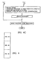
- Figs. 4A-4C show an operational flow chart of the WSM including the instruction path taken under various instruction modes.
- the WSM initiates a read back cycle.
- Each read word-step in the read back cycle has 4 phases as described below.
- Phase 1 The SRAM columns are equalized at about VCC/2. It is during this equalization time that the WSM 77 may change the word addresses without upsetting the SRAM content.
- the core is accessed by the data sense amps 67 and by the parity sense amps 69 and old raw data plus parity bits are presented to the ECC circuit 73.
- Phase 2 When the ECC 73 has completed error correction, it will have valid data on its outputs and a set error signal, ERR 111, if the raw data had to be corrected. At the same time, the SRAM latches the byte flags onto its outputs and will maintain them latched until the next word-step.
- Phase 3 The read back, RB, gate 81 connects the ECC 73 outputs to the write cache 83 inputs while the WSM 77 evaluates the byte flags.
- Phase 4 Each byte in a word has its own SRAM write clock signal, not shown, which arrives from the WSM 77 only if the corresponding byte flag has been read as set during the previous phase. If the byte flag has been read as reset, meaning that this location contains newly loaded data, the write cache SRAM will not receive a write clock for the corresponding byte, so the new loaded data will be preserved in the write cache.
- the WSM 77 monitors the ECC error signal, ERR 111 as shown in phase 2 of Fig. 4A.
- ECC error signal ERR 111
- the WSM will set the page sector flag 47-50 of the corresponding word line latch bank 51-54 if not already set by the load cycle.
- the WSM 77 now starts an on chip high voltage pump, not shown, and then initiates the erase phase. Only the word line latch banks 51-54 with set page sector flags 47-50 will receive the erasing voltages. The corresponding core memory page sectors get erased. The WSM 77 also polls the on chip timer, not shown, to finish this erase phase. At the end of erase time, the WSM 77 performs an erase recovery, i.e. discharges the high voltage on the selected sense line sector segments.
- Phase 1 The SRAM columns are equalized at about VCC/2. It is during this equalization time that the WSM may change the word addresses without upsetting the SRAM content.
- Phase 2 The SRAM sense amps, not shown, read the new data, which until the next word-step will stay latched on the SRAM outputs, 87.
- Phase 3 The ECC 73 is switched into parity generating mode, and its inputs are connected to the SRAM outputs 87 through the data bus, 107.
- This multiplexing function is delivered by the master latch register 71, which has dual inputs controlled by the read back signal RB 103 and the load back signal LB 104. Both RB and LB are controlled by the WSM.
- the ECC 73 output parity bits 89 are ready, and present the valid new parity information onto bus 109 to be written together with the SRAM data bits, 87.
- Phase 4 The SRAM output buffers 87 drive bus 107 and the ECC parity output buffers 89 drive bus 109, which writes the new word into the high voltage page sectors 43-46 through the appropriate Y-select pass transistors 63-66 and core bit lines.
- the WSM 77 initiates the write phase. Again, only word line latch banks 51-54 with set page sector flags 47-50 will send a high programming voltage onto their page sector sense line 99-102. Within each active memory sector 59-62, only the bit lines with set high voltage page latches will actually get the high voltage and thus write to the storage cells on the selected core row. The selected word line 57 also gets the high voltage.
- the WSM 77 polls the on chip timer to finish this write phase. At the end of the write time, the WSM 77 performs a bit line recovery, i.e. discharges the high voltage on the selected bit lines, and then a word line recovery. The WSM 77 now discharges the on chip high voltage pump, and upon exit passes the chip control to the ATD circuitry so that the chip may resume the read mode.
- the circuit of the present invention also implements interruptible load cycles by introducing 3 new bits to the prior art method of polling the write status of a WSM 77. At the beginning of a load cycle, all 3 new status bits are reset and get set at different points during a write cycle as described below. Bit: LOAD TIME-OUT WARNING - Is set after 75% of the total time-out period of a load cycle has expired, and remains set until the exit of the WSM. Bit: ERASE ACTIVE - Is set during the read back and erase phases. Bit: WRITE ACTIVE - Is set during the load back and write phases.
- the final load can actually be empty.
- the chip will observe the regular load cycle time-out interval and proceed with programming. It is precisely because the final load cycle can be empty, that the final load mode can be interrupted. Since the chip is using the on chip timer to count the load time-out, an interrupt will not prevent the chip from entering programming. In fact, immediately after giving the final load plus programming mode ID, the user system can proceed serving another process.
Claims (11)
- Elektrisch löschbarer, programmierbarer Festwertspeicher, EEPROM, mit:einem Hauptspeicherkern, der aus einer Vielzahl von Speicherzellen besteht, die in einer Matrix von Zeilen und Spalten angeordnet sind, wobei die Speicherzellen ferner in eine Vielzahl von Speichereinheiten (31, 35) gruppiert sind, wobei jede Speichereinheit einen Datenwortabschnitt und einen Paritätsbitabschnitt umfasst;einem Datenbus (107) zum Zugreifen auf den Datenwortabschnitt einer Speichereinheit (31, 35);einem Paritätsbus (109) zum Zugreifen auf den Paritätsbitabschnitt einer Speichereinheit (31, 35), wobei der EEPROM-Speicher gekennzeichnet ist durch:einen Hauptzwischenspeicher (71) zum selektiven Einspeichern des Datenbusses (107) und des Paritätsbusses (109);eine Fehlerkorrektur-Steuereinheit (ECC, 73) zum Empfangen des eingespeicherten Datenbusses und Paritätsbusses (109) vom Hauptzwischenspeicher (71), wobei die Fehlerkorrektur-Steuereinheit (73) selektiv eines von entweder einem korrigierten Datenwort entsprechend dem Paritätsbitabschnitt oder ansonsten einem neuen Satz von Paritätsbits entsprechend dem Datenwortabschnitt erzeugt;ein Ausgangsdaten-Leitwegmittel (79) zum selektiven Leiten des korrigierten Datenworts von der Fehlerkorrektur-Steuereinheit (73) zu einem Satz von Eingangs/Ausgangs-Anschlussleitungen; undeinen Schreibcache (83) mit einem Ausgabemittel, das mit dem Datenbus (107) gekoppelt ist, und wobei der Schreibcache (83) selektiv das korrigierte Datenwort von der Fehlerkorrektur-Steuereinheit (73) empfängt.
- Speicher nach Anspruch 1, wobei jeder Datenwortabschnitt aus einem Mehrbyte-Datenwort besteht und ein Verhältnis des Paritätsbit-Zählwerts zum Mehrbyte-Datenwort-Bitzählwert unterhalb 50% liegt.
- Speicher nach Anspruch 1 oder 2, wobei der Speicherkern ferner in individuell löschbare und programmierbare Unterseitensektoren (33) mit einer Vielzahl der Speichereinheiten (31, 35) unterteilt ist, wobei jeder Unterseitensektor (33) durch eine Sektoransteuerleitung festgelegt wird, die über ein Sektoransteuerbauelement (40) mit einer Sektorleseleitung (99-101) gekoppelt ist, die wiederum mit allen Speichereinheiten (31, 35) innerhalb eines Unterseitensektors (33) gekoppelt ist, wobei jeder Unterseitensektor durch das Sektoransteuerbauelement (40) individuell adressierbar ist, wobei jeder Unterseitensektor (33) ein ganzzahliger Teiler einer Speicherseite ist.
- Speicher nach Anspruch 2 oder 3, wobei die Eingangs/Ausgangs-Anschlussleitungen zu einer einzelnen Bytegrößeneinheit gruppiert sind und das Ausgangsleitwegmittel (79) nacheinander jedes Byte eines korrigierten Datenworts von der Fehlerkorrektur-Steuereinheit (73) zur einzelnen Bytegrößeneinheit von Eingangs/Ausgangs-Anschlussleitungen leitet.
- Speicher nach Anspruch 3, welcher ferner eine Seite hoher Spannung zum Übertragen von Programmier- und Löschspannungspegeln zu jeder Speichereinheit (31, 35) der Unterseitensektoren (33) umfasst, wobei die Seite hoher Spannung (43-46) in unabhängige und selektiv aktivierte Bereiche hoher Spannung unterteilt ist, wobei jeder Seitenbereich hoher Spannung die gleiche Größe aufweist wie ein separater Unterseitensektor (33) und diesem entspricht.
- Speicher nach einem der vorangehenden Ansprüche, welcher ferner einen Paritätsbit-Leitwegtreiber (89) zum selektiven Koppeln des neuen Satzes von Paritätsbits von der Fehlerkorrektur-Steuereinheit (73) mit dem Paritätsbus (109) umfasst.
- Speicher nach Anspruch 1, wobei der Schreibcache (83) kleiner ist als der Hauptspeicherkern und in einer Vielzahl von Dateneinheiten mit Ein-Byte-Größe angeordnet ist.
- Speicher nach den Ansprüchen 2 und 7, wobei der Schreibcache (83) ein Mittel zum Annehmen eines separaten Schreibsteuersignals für jedes Datenbyte aufweist.
- Speicher nach Anspruch 7, welcher ferner ein Eingangsdaten-Leitwegmittel zum Empfangen von Bytegrößen-Eingangssignalen von den Eingangs/Ausgangs-Anschlussleitungen, zum Anordnen der Bytegrößen-Eingangssignale in ein Dateneingangswort mit einer Größe gleich einem Datenwortabschnitt einer Speichereinheit (31, 35) und zum sequentiellen Speichern jedes Bytes des Dateneingangsworts im Cache umfasst.
- Speicher nach Anspruch 9, wobei der Schreibcache (83) ferner Cachekennzeichenbits umfasst, wobei selektive Cachekennzeichenbits als Reaktion darauf, dass Daten im Schreibcache (83) gespeichert werden, aktiviert werden.
- Speicher nach Anspruch 10, welcher ferner eine Schreibzustandsmaschine (77) umfasst, die zum Überwachen der Fehlerkorrektur-Steuereinheit (73) gekoppelt ist, und wobei die Schreibzustandsmaschine (77) ein Kennzeichenbit im Schreibcache (83) als Reaktion darauf, dass die Fehlerkorrektur-Steuereinheit (73) ein korrigiertes Datenwort erzeugt, aktiviert.
Applications Claiming Priority (3)
| Application Number | Priority Date | Filing Date | Title |
|---|---|---|---|
| US08/405,884 US5606532A (en) | 1995-03-17 | 1995-03-17 | EEPROM array with flash-like core |
| US405884 | 1995-03-17 | ||
| EP96907103A EP0764330B1 (de) | 1995-03-17 | 1996-02-22 | Eeprom-matrix mit einem, dem "flash"-speicher ähnlichen, kern |
Related Parent Applications (1)
| Application Number | Title | Priority Date | Filing Date |
|---|---|---|---|
| EP96907103A Division EP0764330B1 (de) | 1995-03-17 | 1996-02-22 | Eeprom-matrix mit einem, dem "flash"-speicher ähnlichen, kern |
Publications (2)
| Publication Number | Publication Date |
|---|---|
| EP1158533A1 EP1158533A1 (de) | 2001-11-28 |
| EP1158533B1 true EP1158533B1 (de) | 2003-11-05 |
Family
ID=23605633
Family Applications (2)
| Application Number | Title | Priority Date | Filing Date |
|---|---|---|---|
| EP96907103A Expired - Lifetime EP0764330B1 (de) | 1995-03-17 | 1996-02-22 | Eeprom-matrix mit einem, dem "flash"-speicher ähnlichen, kern |
| EP01117713A Expired - Lifetime EP1158533B1 (de) | 1995-03-17 | 1996-02-22 | EEPROM-Matrix mit einem, dem "Flash"-Speicher ähnlichen Kern |
Family Applications Before (1)
| Application Number | Title | Priority Date | Filing Date |
|---|---|---|---|
| EP96907103A Expired - Lifetime EP0764330B1 (de) | 1995-03-17 | 1996-02-22 | Eeprom-matrix mit einem, dem "flash"-speicher ähnlichen, kern |
Country Status (8)
| Country | Link |
|---|---|
| US (2) | US5606532A (de) |
| EP (2) | EP0764330B1 (de) |
| JP (1) | JPH10500801A (de) |
| KR (1) | KR100348774B1 (de) |
| CN (2) | CN1110053C (de) |
| DE (2) | DE69621201T2 (de) |
| TW (1) | TW309616B (de) |
| WO (1) | WO1996029704A1 (de) |
Cited By (1)
| Publication number | Priority date | Publication date | Assignee | Title |
|---|---|---|---|---|
| CN101303890B (zh) * | 2007-05-10 | 2013-03-13 | 三星电子株式会社 | 包括比较当前和先前区段地址的数据读取方法和有关装置 |
Families Citing this family (172)
| Publication number | Priority date | Publication date | Assignee | Title |
|---|---|---|---|---|
| DE69033438T2 (de) | 1989-04-13 | 2000-07-06 | Sandisk Corp | Austausch von fehlerhaften Speicherzellen einer EEprommatritze |
| US5430859A (en) * | 1991-07-26 | 1995-07-04 | Sundisk Corporation | Solid state memory system including plural memory chips and a serialized bus |
| US5673417A (en) * | 1995-07-20 | 1997-09-30 | Inventec Corporation | Electronic organizer with a flash memory and associated data archiving |
| JP3941149B2 (ja) * | 1996-12-03 | 2007-07-04 | ソニー株式会社 | 半導体不揮発性記憶装置 |
| KR100200922B1 (ko) * | 1995-12-27 | 1999-06-15 | 윤종용 | 반도체 메모리장치의 펌핑전압발생기 |
| US5890192A (en) | 1996-11-05 | 1999-03-30 | Sandisk Corporation | Concurrent write of multiple chunks of data into multiple subarrays of flash EEPROM |
| JP3411186B2 (ja) * | 1997-06-06 | 2003-05-26 | シャープ株式会社 | 不揮発性半導体記憶装置 |
| DE19731954C2 (de) * | 1997-07-24 | 2000-08-24 | Bosch Gmbh Robert | Verfahren zur Erkennung von fehlprogrammierten Speicherzellen eines Speichers |
| US5930167A (en) * | 1997-07-30 | 1999-07-27 | Sandisk Corporation | Multi-state non-volatile flash memory capable of being its own two state write cache |
| TW337607B (en) | 1997-08-06 | 1998-08-01 | Mos Electronics Taiwan Inc | Process for forming a contact hole in an EEPROM with NOR construction |
| US6040216A (en) * | 1997-08-11 | 2000-03-21 | Mosel Vitelic, Inc. | Method (and device) for producing tunnel silicon oxynitride layer |
| US6000006A (en) * | 1997-08-25 | 1999-12-07 | Bit Microsystems, Inc. | Unified re-map and cache-index table with dual write-counters for wear-leveling of non-volatile flash RAM mass storage |
| JPH11176158A (ja) * | 1997-12-10 | 1999-07-02 | Fujitsu Ltd | ラッチ回路、データ出力回路及びこれを有する半導体装置 |
| TW425660B (en) | 1997-12-12 | 2001-03-11 | Mosel Vitelic Inc | Method of forming uniform dielectric layer between two conductive layers in integrated circuit |
| TW374939B (en) | 1997-12-19 | 1999-11-21 | Promos Technologies Inc | Method of formation of 2 gate oxide layers of different thickness in an IC |
| KR100266748B1 (ko) * | 1997-12-31 | 2000-10-02 | 윤종용 | 반도체 메모리 장치 및 그 장치의 에러 정정 방법 |
| TW382801B (en) | 1998-02-25 | 2000-02-21 | Mosel Vitelic Inc | Method of forming two transistors having different threshold voltage in integrated circuit |
| TW480713B (en) * | 1998-03-03 | 2002-03-21 | Mosel Vitelic Inc | Method for forming different thickness of field oxide in integrated circuit and the structure of the same |
| US6136653A (en) * | 1998-05-11 | 2000-10-24 | Mosel Vitelic, Inc. | Method and device for producing undercut gate for flash memory |
| US6261903B1 (en) | 1998-05-14 | 2001-07-17 | Mosel Vitelic, Inc. | Floating gate method and device |
| US6365455B1 (en) | 1998-06-05 | 2002-04-02 | Mosel Vitelic, Inc. | Flash memory process using polysilicon spacers |
| JP2002532813A (ja) * | 1998-06-24 | 2002-10-02 | インフィニオン テクノロジーズ アクチエンゲゼルシャフト | 電子式メモリ装置 |
| JP3999900B2 (ja) | 1998-09-10 | 2007-10-31 | 株式会社東芝 | 不揮発性半導体メモリ |
| US6088268A (en) * | 1998-09-17 | 2000-07-11 | Atmel Corporation | Flash memory array with internal refresh |
| JP4074029B2 (ja) | 1999-06-28 | 2008-04-09 | 株式会社東芝 | フラッシュメモリ |
| FR2798767B1 (fr) * | 1999-09-16 | 2001-12-14 | St Microelectronics Sa | Procede d'ecriture en mode page d'une memoire non volatile electriquement programmable/effacable et architecture correspondante |
| FR2802012B1 (fr) * | 1999-12-07 | 2002-02-15 | St Microelectronics Sa | Memoire dram rapide |
| US6728913B1 (en) * | 2000-02-25 | 2004-04-27 | Advanced Micro Devices, Inc. | Data recycling in memory |
| US6731538B2 (en) * | 2000-03-10 | 2004-05-04 | Kabushiki Kaisha Toshiba | Semiconductor memory device including page latch circuit |
| JP2001297038A (ja) | 2000-04-11 | 2001-10-26 | Toshiba Corp | データ記憶装置および記録媒体並びに記録媒体制御方法 |
| US6950336B2 (en) * | 2000-05-03 | 2005-09-27 | Emosyn America, Inc. | Method and apparatus for emulating an electrically erasable programmable read only memory (EEPROM) using non-volatile floating gate memory cells |
| US6400603B1 (en) | 2000-05-03 | 2002-06-04 | Advanced Technology Materials, Inc. | Electronically-eraseable programmable read-only memory having reduced-page-size program and erase |
| FR2809222A1 (fr) * | 2000-05-17 | 2001-11-23 | St Microelectronics Sa | Memoire eeprom comprenant un systeme de correction d'erreur |
| EP1233421B1 (de) * | 2001-02-19 | 2007-07-11 | STMicroelectronics S.r.l. | Verfahren zur Auffrischung der gespeicherten Daten in einem elektrisch lösch- und programmierbaren nichtflüchtigen Speicher |
| JP4530562B2 (ja) * | 2001-03-27 | 2010-08-25 | ローム株式会社 | 不揮発性メモリ |
| US6717847B2 (en) * | 2001-09-17 | 2004-04-06 | Sandisk Corporation | Selective operation of a multi-state non-volatile memory system in a binary mode |
| US6456528B1 (en) | 2001-09-17 | 2002-09-24 | Sandisk Corporation | Selective operation of a multi-state non-volatile memory system in a binary mode |
| US6683817B2 (en) * | 2002-02-21 | 2004-01-27 | Qualcomm, Incorporated | Direct memory swapping between NAND flash and SRAM with error correction coding |
| US6751127B1 (en) | 2002-04-24 | 2004-06-15 | Macronix International, Co. Ltd. | Systems and methods for refreshing non-volatile memory |
| US6633500B1 (en) | 2002-04-26 | 2003-10-14 | Macronix International Co., Ltd. | Systems and methods for refreshing a non-volatile memory using a token |
| JP4257824B2 (ja) * | 2002-07-03 | 2009-04-22 | シャープ株式会社 | 半導体記憶装置 |
| US7061792B1 (en) * | 2002-08-10 | 2006-06-13 | National Semiconductor Corporation | Low AC power SRAM architecture |
| US20040153902A1 (en) * | 2003-01-21 | 2004-08-05 | Nexflash Technologies, Inc. | Serial flash integrated circuit having error detection and correction |
| US6996688B2 (en) * | 2003-03-11 | 2006-02-07 | International Business Machines Corporation | Method, system, and program for improved throughput in remote mirroring systems |
| CN1311366C (zh) * | 2003-05-22 | 2007-04-18 | 群联电子股份有限公司 | 快闪存储器的平行双轨使用方法 |
| EP1510924B1 (de) * | 2003-08-27 | 2008-07-23 | ARM Limited | Vorrichtung und Verfahren zur Verwaltung von Transaktionen zum Schreiben und Lesen auf EEPROM-Speicher oder Flash-Speicher |
| US7640370B1 (en) * | 2003-11-25 | 2009-12-29 | Marvell International Ltd. | Method and apparatus for controlling data transfer between EEPROM and a physical layer device |
| US7173863B2 (en) * | 2004-03-08 | 2007-02-06 | Sandisk Corporation | Flash controller cache architecture |
| US7099221B2 (en) | 2004-05-06 | 2006-08-29 | Micron Technology, Inc. | Memory controller method and system compensating for memory cell data losses |
| JP4135680B2 (ja) * | 2004-05-31 | 2008-08-20 | ソニー株式会社 | 半導体記憶装置および信号処理システム |
| US20060010339A1 (en) * | 2004-06-24 | 2006-01-12 | Klein Dean A | Memory system and method having selective ECC during low power refresh |
| US7340668B2 (en) * | 2004-06-25 | 2008-03-04 | Micron Technology, Inc. | Low power cost-effective ECC memory system and method |
| US7116602B2 (en) | 2004-07-15 | 2006-10-03 | Micron Technology, Inc. | Method and system for controlling refresh to avoid memory cell data losses |
| US6965537B1 (en) * | 2004-08-31 | 2005-11-15 | Micron Technology, Inc. | Memory system and method using ECC to achieve low power refresh |
| US7882299B2 (en) * | 2004-12-21 | 2011-02-01 | Sandisk Corporation | System and method for use of on-chip non-volatile memory write cache |
| US7212440B2 (en) * | 2004-12-30 | 2007-05-01 | Sandisk Corporation | On-chip data grouping and alignment |
| TWI263229B (en) * | 2005-03-17 | 2006-10-01 | Sunplus Technology Co Ltd | Memory device with interface for serial transmission and error correction method for serial transmission interface |
| KR100680473B1 (ko) * | 2005-04-11 | 2007-02-08 | 주식회사 하이닉스반도체 | 액세스 시간이 감소된 플래시 메모리 장치 |
| JP4761910B2 (ja) * | 2005-10-05 | 2011-08-31 | 株式会社東芝 | 不揮発性半導体記憶装置及びそれを用いた不揮発性メモリシステム |
| JP4910360B2 (ja) * | 2005-10-20 | 2012-04-04 | ソニー株式会社 | 記憶装置、コンピュータシステム、およびデータ書き込み方法 |
| US7447096B2 (en) * | 2006-05-05 | 2008-11-04 | Honeywell International Inc. | Method for refreshing a non-volatile memory |
| US7471562B2 (en) * | 2006-05-08 | 2008-12-30 | Macronix International Co., Ltd. | Method and apparatus for accessing nonvolatile memory with read error by changing read reference |
| US7773421B2 (en) * | 2006-05-08 | 2010-08-10 | Macronix International Co., Ltd. | Method and apparatus for accessing memory with read error by changing comparison |
| US8077516B2 (en) * | 2006-05-08 | 2011-12-13 | Macronix International Co., Ltd. | Method and apparatus for accessing memory with read error by changing comparison |
| US8997255B2 (en) | 2006-07-31 | 2015-03-31 | Inside Secure | Verifying data integrity in a data storage device |
| US7567461B2 (en) | 2006-08-18 | 2009-07-28 | Micron Technology, Inc. | Method and system for minimizing number of programming pulses used to program rows of non-volatile memory cells |
| US8352752B2 (en) * | 2006-09-01 | 2013-01-08 | Inside Secure | Detecting radiation-based attacks |
| US7894289B2 (en) | 2006-10-11 | 2011-02-22 | Micron Technology, Inc. | Memory system and method using partial ECC to achieve low power refresh and fast access to data |
| US7900120B2 (en) | 2006-10-18 | 2011-03-01 | Micron Technology, Inc. | Memory system and method using ECC with flag bit to identify modified data |
| US8060688B2 (en) * | 2006-12-07 | 2011-11-15 | Nxp B.V. | Method and device for reconfiguration of reliability data in flash EEPROM storage pages |
| JP5018074B2 (ja) * | 2006-12-22 | 2012-09-05 | 富士通セミコンダクター株式会社 | メモリ装置,メモリコントローラ及びメモリシステム |
| KR100819102B1 (ko) * | 2007-02-06 | 2008-04-03 | 삼성전자주식회사 | 개선된 멀티 페이지 프로그램 동작을 갖는 불휘발성 반도체메모리 장치 |
| KR100888482B1 (ko) | 2007-05-11 | 2009-03-12 | 삼성전자주식회사 | 비휘발성 반도체 메모리 장치 및 상기 비휘발성 반도체메모리 장치의 쓰기 방법 |
| KR101472797B1 (ko) * | 2007-07-16 | 2014-12-15 | 삼성전자주식회사 | 데이터를 읽거나 쓰기 위한 방법 및 장치 |
| KR101425957B1 (ko) * | 2007-08-21 | 2014-08-06 | 삼성전자주식회사 | 이씨씨 제어 회로 및 그것을 포함하는 멀티채널 메모리시스템 |
| JP2009104757A (ja) * | 2007-10-02 | 2009-05-14 | Panasonic Corp | 半導体記憶装置 |
| JP5049733B2 (ja) * | 2007-10-17 | 2012-10-17 | 株式会社東芝 | 情報処理システム |
| US8959307B1 (en) | 2007-11-16 | 2015-02-17 | Bitmicro Networks, Inc. | Reduced latency memory read transactions in storage devices |
| US8775717B2 (en) | 2007-12-27 | 2014-07-08 | Sandisk Enterprise Ip Llc | Storage controller for flash memory including a crossbar switch connecting a plurality of processors with a plurality of internal memories |
| KR101483190B1 (ko) | 2008-09-05 | 2015-01-19 | 삼성전자주식회사 | 메모리 시스템 및 그것의 데이터 처리 방법 |
| EP2267724A1 (de) * | 2009-06-26 | 2010-12-29 | STMicroelectronics Rousset SAS | EEPROM Speicher-Architektur optimiert für eingebettete Speicher |
| US9135190B1 (en) | 2009-09-04 | 2015-09-15 | Bitmicro Networks, Inc. | Multi-profile memory controller for computing devices |
| US8665601B1 (en) | 2009-09-04 | 2014-03-04 | Bitmicro Networks, Inc. | Solid state drive with improved enclosure assembly |
| US8447908B2 (en) | 2009-09-07 | 2013-05-21 | Bitmicro Networks, Inc. | Multilevel memory bus system for solid-state mass storage |
| US8560804B2 (en) | 2009-09-14 | 2013-10-15 | Bitmicro Networks, Inc. | Reducing erase cycles in an electronic storage device that uses at least one erase-limited memory device |
| WO2011067795A1 (en) * | 2009-12-02 | 2011-06-09 | Ferdinando Bedeschi | Refresh architecture and algorithm for non-volatile memories |
| US20120246384A1 (en) * | 2011-03-21 | 2012-09-27 | Winbond Electronics Corp. | Flash memory and flash memory accessing method |
| CN102339644B (zh) * | 2011-07-27 | 2014-12-24 | 聚辰半导体(上海)有限公司 | 存储器及其操作方法 |
| US9372755B1 (en) | 2011-10-05 | 2016-06-21 | Bitmicro Networks, Inc. | Adaptive power cycle sequences for data recovery |
| US8793543B2 (en) * | 2011-11-07 | 2014-07-29 | Sandisk Enterprise Ip Llc | Adaptive read comparison signal generation for memory systems |
| EP2608036A1 (de) * | 2011-12-22 | 2013-06-26 | Thomson Licensing | Verfahren und System zum Verwalten der Fehlererkennung und -korrektur |
| US9043669B1 (en) | 2012-05-18 | 2015-05-26 | Bitmicro Networks, Inc. | Distributed ECC engine for storage media |
| CN102768859A (zh) * | 2012-07-12 | 2012-11-07 | 深圳市锐能微科技有限公司 | 一种eeprom擦写控制装置 |
| US9699263B1 (en) | 2012-08-17 | 2017-07-04 | Sandisk Technologies Llc. | Automatic read and write acceleration of data accessed by virtual machines |
| JP5853906B2 (ja) * | 2012-08-24 | 2016-02-09 | ソニー株式会社 | 記憶制御装置、記憶装置、情報処理システムおよび記憶制御方法 |
| US9123401B2 (en) * | 2012-10-15 | 2015-09-01 | Silicon Storage Technology, Inc. | Non-volatile memory array and method of using same for fractional word programming |
| US9472284B2 (en) | 2012-11-19 | 2016-10-18 | Silicon Storage Technology, Inc. | Three-dimensional flash memory system |
| US9501398B2 (en) | 2012-12-26 | 2016-11-22 | Sandisk Technologies Llc | Persistent storage device with NVRAM for staging writes |
| US9239751B1 (en) | 2012-12-27 | 2016-01-19 | Sandisk Enterprise Ip Llc | Compressing data from multiple reads for error control management in memory systems |
| US9612948B2 (en) | 2012-12-27 | 2017-04-04 | Sandisk Technologies Llc | Reads and writes between a contiguous data block and noncontiguous sets of logical address blocks in a persistent storage device |
| US9003264B1 (en) | 2012-12-31 | 2015-04-07 | Sandisk Enterprise Ip Llc | Systems, methods, and devices for multi-dimensional flash RAID data protection |
| US9454420B1 (en) | 2012-12-31 | 2016-09-27 | Sandisk Technologies Llc | Method and system of reading threshold voltage equalization |
| US9870830B1 (en) | 2013-03-14 | 2018-01-16 | Sandisk Technologies Llc | Optimal multilevel sensing for reading data from a storage medium |
| US9423457B2 (en) | 2013-03-14 | 2016-08-23 | Bitmicro Networks, Inc. | Self-test solution for delay locked loops |
| US9971524B1 (en) | 2013-03-15 | 2018-05-15 | Bitmicro Networks, Inc. | Scatter-gather approach for parallel data transfer in a mass storage system |
| US9400617B2 (en) | 2013-03-15 | 2016-07-26 | Bitmicro Networks, Inc. | Hardware-assisted DMA transfer with dependency table configured to permit-in parallel-data drain from cache without processor intervention when filled or drained |
| US9934045B1 (en) | 2013-03-15 | 2018-04-03 | Bitmicro Networks, Inc. | Embedded system boot from a storage device |
| US9875205B1 (en) | 2013-03-15 | 2018-01-23 | Bitmicro Networks, Inc. | Network of memory systems |
| US9916213B1 (en) | 2013-03-15 | 2018-03-13 | Bitmicro Networks, Inc. | Bus arbitration with routing and failover mechanism |
| US9367246B2 (en) | 2013-03-15 | 2016-06-14 | Sandisk Technologies Inc. | Performance optimization of data transfer for soft information generation |
| US10120694B2 (en) | 2013-03-15 | 2018-11-06 | Bitmicro Networks, Inc. | Embedded system boot from a storage device |
| US10489318B1 (en) | 2013-03-15 | 2019-11-26 | Bitmicro Networks, Inc. | Scatter-gather approach for parallel data transfer in a mass storage system |
| US9236886B1 (en) | 2013-03-15 | 2016-01-12 | Sandisk Enterprise Ip Llc | Universal and reconfigurable QC-LDPC encoder |
| US9092350B1 (en) | 2013-03-15 | 2015-07-28 | Sandisk Enterprise Ip Llc | Detection and handling of unbalanced errors in interleaved codewords |
| US9501436B1 (en) | 2013-03-15 | 2016-11-22 | Bitmicro Networks, Inc. | Multi-level message passing descriptor |
| US9720603B1 (en) | 2013-03-15 | 2017-08-01 | Bitmicro Networks, Inc. | IOC to IOC distributed caching architecture |
| US9136877B1 (en) | 2013-03-15 | 2015-09-15 | Sandisk Enterprise Ip Llc | Syndrome layered decoding for LDPC codes |
| US9430386B2 (en) | 2013-03-15 | 2016-08-30 | Bitmicro Networks, Inc. | Multi-leveled cache management in a hybrid storage system |
| US9798688B1 (en) | 2013-03-15 | 2017-10-24 | Bitmicro Networks, Inc. | Bus arbitration with routing and failover mechanism |
| US9244763B1 (en) | 2013-03-15 | 2016-01-26 | Sandisk Enterprise Ip Llc | System and method for updating a reading threshold voltage based on symbol transition information |
| US9734067B1 (en) | 2013-03-15 | 2017-08-15 | Bitmicro Networks, Inc. | Write buffering |
| US9672178B1 (en) | 2013-03-15 | 2017-06-06 | Bitmicro Networks, Inc. | Bit-mapped DMA transfer with dependency table configured to monitor status so that a processor is not rendered as a bottleneck in a system |
| US9842024B1 (en) | 2013-03-15 | 2017-12-12 | Bitmicro Networks, Inc. | Flash electronic disk with RAID controller |
| US9159437B2 (en) | 2013-06-11 | 2015-10-13 | Sandisk Enterprise IP LLC. | Device and method for resolving an LM flag issue |
| US9384126B1 (en) | 2013-07-25 | 2016-07-05 | Sandisk Technologies Inc. | Methods and systems to avoid false negative results in bloom filters implemented in non-volatile data storage systems |
| US9043517B1 (en) | 2013-07-25 | 2015-05-26 | Sandisk Enterprise Ip Llc | Multipass programming in buffers implemented in non-volatile data storage systems |
| US9524235B1 (en) | 2013-07-25 | 2016-12-20 | Sandisk Technologies Llc | Local hash value generation in non-volatile data storage systems |
| US9235509B1 (en) | 2013-08-26 | 2016-01-12 | Sandisk Enterprise Ip Llc | Write amplification reduction by delaying read access to data written during garbage collection |
| US9639463B1 (en) | 2013-08-26 | 2017-05-02 | Sandisk Technologies Llc | Heuristic aware garbage collection scheme in storage systems |
| US9298608B2 (en) | 2013-10-18 | 2016-03-29 | Sandisk Enterprise Ip Llc | Biasing for wear leveling in storage systems |
| US9442662B2 (en) | 2013-10-18 | 2016-09-13 | Sandisk Technologies Llc | Device and method for managing die groups |
| US9436831B2 (en) | 2013-10-30 | 2016-09-06 | Sandisk Technologies Llc | Secure erase in a memory device |
| US9263156B2 (en) | 2013-11-07 | 2016-02-16 | Sandisk Enterprise Ip Llc | System and method for adjusting trip points within a storage device |
| US9244785B2 (en) | 2013-11-13 | 2016-01-26 | Sandisk Enterprise Ip Llc | Simulated power failure and data hardening |
| US9703816B2 (en) | 2013-11-19 | 2017-07-11 | Sandisk Technologies Llc | Method and system for forward reference logging in a persistent datastore |
| US9520197B2 (en) | 2013-11-22 | 2016-12-13 | Sandisk Technologies Llc | Adaptive erase of a storage device |
| US9520162B2 (en) | 2013-11-27 | 2016-12-13 | Sandisk Technologies Llc | DIMM device controller supervisor |
| US9582058B2 (en) | 2013-11-29 | 2017-02-28 | Sandisk Technologies Llc | Power inrush management of storage devices |
| US9235245B2 (en) | 2013-12-04 | 2016-01-12 | Sandisk Enterprise Ip Llc | Startup performance and power isolation |
| US9129665B2 (en) | 2013-12-17 | 2015-09-08 | Sandisk Enterprise Ip Llc | Dynamic brownout adjustment in a storage device |
| US9703636B2 (en) | 2014-03-01 | 2017-07-11 | Sandisk Technologies Llc | Firmware reversion trigger and control |
| US9685242B2 (en) * | 2014-03-11 | 2017-06-20 | Kabushiki Kaisha Toshiba | Memory system |
| US9448876B2 (en) | 2014-03-19 | 2016-09-20 | Sandisk Technologies Llc | Fault detection and prediction in storage devices |
| US9454448B2 (en) | 2014-03-19 | 2016-09-27 | Sandisk Technologies Llc | Fault testing in storage devices |
| US9390814B2 (en) | 2014-03-19 | 2016-07-12 | Sandisk Technologies Llc | Fault detection and prediction for data storage elements |
| US9390021B2 (en) | 2014-03-31 | 2016-07-12 | Sandisk Technologies Llc | Efficient cache utilization in a tiered data structure |
| US9626399B2 (en) | 2014-03-31 | 2017-04-18 | Sandisk Technologies Llc | Conditional updates for reducing frequency of data modification operations |
| US9626400B2 (en) | 2014-03-31 | 2017-04-18 | Sandisk Technologies Llc | Compaction of information in tiered data structure |
| US9697267B2 (en) | 2014-04-03 | 2017-07-04 | Sandisk Technologies Llc | Methods and systems for performing efficient snapshots in tiered data structures |
| US10055150B1 (en) | 2014-04-17 | 2018-08-21 | Bitmicro Networks, Inc. | Writing volatile scattered memory metadata to flash device |
| US10025736B1 (en) | 2014-04-17 | 2018-07-17 | Bitmicro Networks, Inc. | Exchange message protocol message transmission between two devices |
| US10078604B1 (en) | 2014-04-17 | 2018-09-18 | Bitmicro Networks, Inc. | Interrupt coalescing |
| US9952991B1 (en) | 2014-04-17 | 2018-04-24 | Bitmicro Networks, Inc. | Systematic method on queuing of descriptors for multiple flash intelligent DMA engine operation |
| US9811461B1 (en) | 2014-04-17 | 2017-11-07 | Bitmicro Networks, Inc. | Data storage system |
| US10042792B1 (en) | 2014-04-17 | 2018-08-07 | Bitmicro Networks, Inc. | Method for transferring and receiving frames across PCI express bus for SSD device |
| US9070481B1 (en) | 2014-05-30 | 2015-06-30 | Sandisk Technologies Inc. | Internal current measurement for age measurements |
| US9703491B2 (en) | 2014-05-30 | 2017-07-11 | Sandisk Technologies Llc | Using history of unaligned writes to cache data and avoid read-modify-writes in a non-volatile storage device |
| US10656842B2 (en) | 2014-05-30 | 2020-05-19 | Sandisk Technologies Llc | Using history of I/O sizes and I/O sequences to trigger coalesced writes in a non-volatile storage device |
| US10146448B2 (en) | 2014-05-30 | 2018-12-04 | Sandisk Technologies Llc | Using history of I/O sequences to trigger cached read ahead in a non-volatile storage device |
| US10162748B2 (en) | 2014-05-30 | 2018-12-25 | Sandisk Technologies Llc | Prioritizing garbage collection and block allocation based on I/O history for logical address regions |
| US10656840B2 (en) | 2014-05-30 | 2020-05-19 | Sandisk Technologies Llc | Real-time I/O pattern recognition to enhance performance and endurance of a storage device |
| US10372613B2 (en) | 2014-05-30 | 2019-08-06 | Sandisk Technologies Llc | Using sub-region I/O history to cache repeatedly accessed sub-regions in a non-volatile storage device |
| US10114557B2 (en) | 2014-05-30 | 2018-10-30 | Sandisk Technologies Llc | Identification of hot regions to enhance performance and endurance of a non-volatile storage device |
| US9093160B1 (en) | 2014-05-30 | 2015-07-28 | Sandisk Technologies Inc. | Methods and systems for staggered memory operations |
| US9652381B2 (en) | 2014-06-19 | 2017-05-16 | Sandisk Technologies Llc | Sub-block garbage collection |
| US9443601B2 (en) | 2014-09-08 | 2016-09-13 | Sandisk Technologies Llc | Holdup capacitor energy harvesting |
| JP6411282B2 (ja) * | 2015-05-15 | 2018-10-24 | ラピスセミコンダクタ株式会社 | 半導体メモリ及びデータ書込方法 |
| FR3039922B1 (fr) * | 2015-08-06 | 2018-02-02 | Stmicroelectronics (Rousset) Sas | Procede d'ecriture dans une memoire du type eeprom et dispositif de memoire correspondant |
| US9910749B2 (en) | 2016-06-23 | 2018-03-06 | Sandisk Technologies Llc | Non-volatile memory with dynamic repurpose of word line |
| US10290353B2 (en) | 2016-09-06 | 2019-05-14 | Western Digital Technologies, Inc. | Error mitigation for 3D NAND flash memory |
| US10552050B1 (en) | 2017-04-07 | 2020-02-04 | Bitmicro Llc | Multi-dimensional computer storage system |
| US11256616B2 (en) * | 2019-12-24 | 2022-02-22 | Micron Technology, Inc. | Power loss data protection in a memory sub-system |
Family Cites Families (16)
| Publication number | Priority date | Publication date | Assignee | Title |
|---|---|---|---|---|
| US4949309A (en) * | 1988-05-11 | 1990-08-14 | Catalyst Semiconductor, Inc. | EEPROM utilizing single transistor per cell capable of both byte erase and flash erase |
| DE69033438T2 (de) * | 1989-04-13 | 2000-07-06 | Sandisk Corp | Austausch von fehlerhaften Speicherzellen einer EEprommatritze |
| US5535328A (en) * | 1989-04-13 | 1996-07-09 | Sandisk Corporation | Non-volatile memory system card with flash erasable sectors of EEprom cells including a mechanism for substituting defective cells |
| US5191556A (en) * | 1991-03-13 | 1993-03-02 | Advanced Micro Devices, Inc. | Method of page-mode programming flash eeprom cell arrays |
| US5359569A (en) * | 1991-10-29 | 1994-10-25 | Hitachi Ltd. | Semiconductor memory |
| TW231343B (de) * | 1992-03-17 | 1994-10-01 | Hitachi Seisakusyo Kk | |
| US5353248A (en) * | 1992-04-14 | 1994-10-04 | Altera Corporation | EEPROM-backed FIFO memory |
| US5317535A (en) * | 1992-06-19 | 1994-05-31 | Intel Corporation | Gate/source disturb protection for sixteen-bit flash EEPROM memory arrays |
| JP3328321B2 (ja) * | 1992-06-22 | 2002-09-24 | 株式会社日立製作所 | 半導体記憶装置 |
| JPH0683716A (ja) * | 1992-09-01 | 1994-03-25 | Rohm Co Ltd | 電気的書換可能型不揮発メモリ |
| JPH0750558B2 (ja) * | 1992-09-22 | 1995-05-31 | インターナショナル・ビジネス・マシーンズ・コーポレイション | 一括消去型不揮発性メモリ |
| KR960000616B1 (ko) * | 1993-01-13 | 1996-01-10 | 삼성전자주식회사 | 불휘발성 반도체 메모리 장치 |
| US5488711A (en) * | 1993-04-01 | 1996-01-30 | Microchip Technology Incorporated | Serial EEPROM device and associated method for reducing data load time using a page mode write cache |
| US5363334A (en) * | 1993-04-10 | 1994-11-08 | Microchip Technology Incorporated | Write protection security for memory device |
| US5353256A (en) * | 1993-06-30 | 1994-10-04 | Intel Corporation | Block specific status information in a memory device |
| US5424997A (en) * | 1994-03-15 | 1995-06-13 | National Semiconductor Corporation | Non-volatile semiconductor memory having switching devices for segmentation of a memory page and a method thereof |
-
1995
- 1995-03-17 US US08/405,884 patent/US5606532A/en not_active Expired - Lifetime
-
1996
- 1996-02-22 EP EP96907103A patent/EP0764330B1/de not_active Expired - Lifetime
- 1996-02-22 JP JP8528421A patent/JPH10500801A/ja not_active Ceased
- 1996-02-22 DE DE69621201T patent/DE69621201T2/de not_active Expired - Lifetime
- 1996-02-22 KR KR1019960705804A patent/KR100348774B1/ko not_active IP Right Cessation
- 1996-02-22 CN CN96190070A patent/CN1110053C/zh not_active Expired - Fee Related
- 1996-02-22 WO PCT/US1996/002482 patent/WO1996029704A1/en active IP Right Grant
- 1996-02-22 CN CNB031060390A patent/CN100483548C/zh not_active Expired - Fee Related
- 1996-02-22 EP EP01117713A patent/EP1158533B1/de not_active Expired - Lifetime
- 1996-02-22 DE DE69630624T patent/DE69630624T2/de not_active Expired - Lifetime
- 1996-03-07 TW TW085102771A patent/TW309616B/zh not_active IP Right Cessation
- 1996-09-16 US US08/714,605 patent/US5765185A/en not_active Expired - Lifetime
Cited By (1)
| Publication number | Priority date | Publication date | Assignee | Title |
|---|---|---|---|---|
| CN101303890B (zh) * | 2007-05-10 | 2013-03-13 | 三星电子株式会社 | 包括比较当前和先前区段地址的数据读取方法和有关装置 |
Also Published As
| Publication number | Publication date |
|---|---|
| US5765185A (en) | 1998-06-09 |
| DE69630624T2 (de) | 2004-07-29 |
| EP1158533A1 (de) | 2001-11-28 |
| CN100483548C (zh) | 2009-04-29 |
| DE69630624D1 (de) | 2003-12-11 |
| KR970702561A (ko) | 1997-05-13 |
| EP0764330B1 (de) | 2002-05-15 |
| JPH10500801A (ja) | 1998-01-20 |
| CN1145684A (zh) | 1997-03-19 |
| EP0764330A1 (de) | 1997-03-26 |
| WO1996029704A1 (en) | 1996-09-26 |
| TW309616B (de) | 1997-07-01 |
| DE69621201D1 (de) | 2002-06-20 |
| EP0764330A4 (de) | 2000-07-19 |
| CN1607609A (zh) | 2005-04-20 |
| US5606532A (en) | 1997-02-25 |
| CN1110053C (zh) | 2003-05-28 |
| KR100348774B1 (ko) | 2003-01-24 |
| DE69621201T2 (de) | 2002-12-19 |
Similar Documents
| Publication | Publication Date | Title |
|---|---|---|
| EP1158533B1 (de) | EEPROM-Matrix mit einem, dem "Flash"-Speicher ähnlichen Kern | |
| EP0914659B1 (de) | Kombinierter nichtflüchtiger programm-/datenspeicher für gleichzeitiges lesen von programmen und schreiben von daten | |
| EP0675502B1 (de) | EEPROM-System mit aus mehreren Chips bestehender Blocklöschung | |
| US7405985B2 (en) | Flexible and area efficient column redundancy for non-volatile memories | |
| KR100359414B1 (ko) | 데이타독출/기록방법및그를이용한메모리제어장치및시스템 | |
| EP1242868B1 (de) | Ordnung von blöcken innerhalb eines nicht-flüchtligen speichers zur erheblichen reduzierung der schreibezeit in einem sektor | |
| US5519847A (en) | Method of pipelining sequential writes in a flash memory | |
| US6507885B2 (en) | Memory system, method and predecoding circuit operable in different modes for selectively accessing multiple blocks of memory cells for simultaneous writing or erasure | |
| US7379363B2 (en) | Method and apparatus for implementing high speed memory | |
| US5787484A (en) | System and method which compares data preread from memory cells to data to be written to the cells | |
| EP2256637A1 (de) | Datenkopierung und -ausrichtung auf dem Chip | |
| US20080046639A1 (en) | Memory system with nonvolatile semiconductor memory | |
| US20020085418A1 (en) | Nonvolatile memory system | |
| US5715423A (en) | Memory device with an internal data transfer circuit | |
| EP0960423B1 (de) | Wiederprogrammierbare speichereinrichtung mit variablem seitenformat | |
| US7606993B2 (en) | Flash memory controller, memory control circuit, flash memory system, and method for controlling data exchange between host computer and flash memory | |
| JP4670370B2 (ja) | メモリコントローラ及びフラッシュメモリシステム | |
| US6622201B1 (en) | Chained array of sequential access memories enabling continuous read | |
| KR100480653B1 (ko) | 프로그램판독/데이터기록을동시에수행하는능력을갖는결합된프로그램및데이터비휘발성메모리 | |
| EP0505051A1 (de) | Datenspeichersystem mit intrinsischer Burst-Detektion | |
| JPH05342891A (ja) | 不揮発性半導体記憶装置 |
Legal Events
| Date | Code | Title | Description |
|---|---|---|---|
| PUAI | Public reference made under article 153(3) epc to a published international application that has entered the european phase |
Free format text: ORIGINAL CODE: 0009012 |
|
| AC | Divisional application: reference to earlier application |
Ref document number: 764330 Country of ref document: EP |
|
| AK | Designated contracting states |
Kind code of ref document: A1 Designated state(s): DE FR GB IT NL |
|
| 17P | Request for examination filed |
Effective date: 20020308 |
|
| AKX | Designation fees paid |
Free format text: DE FR GB IT NL |
|
| GRAH | Despatch of communication of intention to grant a patent |
Free format text: ORIGINAL CODE: EPIDOS IGRA |
|
| GRAS | Grant fee paid |
Free format text: ORIGINAL CODE: EPIDOSNIGR3 |
|
| GRAA | (expected) grant |
Free format text: ORIGINAL CODE: 0009210 |
|
| AC | Divisional application: reference to earlier application |
Ref document number: 0764330 Country of ref document: EP Kind code of ref document: P |
|
| AK | Designated contracting states |
Kind code of ref document: B1 Designated state(s): DE FR GB IT NL |
|
| REG | Reference to a national code |
Ref country code: GB Ref legal event code: FG4D |
|
| REF | Corresponds to: |
Ref document number: 69630624 Country of ref document: DE Date of ref document: 20031211 Kind code of ref document: P |
|
| ET | Fr: translation filed | ||
| PLBE | No opposition filed within time limit |
Free format text: ORIGINAL CODE: 0009261 |
|
| STAA | Information on the status of an ep patent application or granted ep patent |
Free format text: STATUS: NO OPPOSITION FILED WITHIN TIME LIMIT |
|
| 26N | No opposition filed |
Effective date: 20040806 |
|
| PGFP | Annual fee paid to national office [announced via postgrant information from national office to epo] |
Ref country code: IT Payment date: 20080227 Year of fee payment: 12 |
|
| PGFP | Annual fee paid to national office [announced via postgrant information from national office to epo] |
Ref country code: NL Payment date: 20090224 Year of fee payment: 14 |
|
| PGFP | Annual fee paid to national office [announced via postgrant information from national office to epo] |
Ref country code: GB Payment date: 20090227 Year of fee payment: 14 |
|
| PG25 | Lapsed in a contracting state [announced via postgrant information from national office to epo] |
Ref country code: IT Free format text: LAPSE BECAUSE OF NON-PAYMENT OF DUE FEES Effective date: 20080222 |
|
| PGFP | Annual fee paid to national office [announced via postgrant information from national office to epo] |
Ref country code: FR Payment date: 20090217 Year of fee payment: 14 |
|
| REG | Reference to a national code |
Ref country code: NL Ref legal event code: V1 Effective date: 20100901 |
|
| GBPC | Gb: european patent ceased through non-payment of renewal fee |
Effective date: 20100222 |
|
| REG | Reference to a national code |
Ref country code: FR Ref legal event code: ST Effective date: 20101029 |
|
| PG25 | Lapsed in a contracting state [announced via postgrant information from national office to epo] |
Ref country code: NL Free format text: LAPSE BECAUSE OF NON-PAYMENT OF DUE FEES Effective date: 20100901 Ref country code: FR Free format text: LAPSE BECAUSE OF NON-PAYMENT OF DUE FEES Effective date: 20100301 |
|
| PG25 | Lapsed in a contracting state [announced via postgrant information from national office to epo] |
Ref country code: GB Free format text: LAPSE BECAUSE OF NON-PAYMENT OF DUE FEES Effective date: 20100222 |
|
| PGFP | Annual fee paid to national office [announced via postgrant information from national office to epo] |
Ref country code: DE Payment date: 20130220 Year of fee payment: 18 |
|
| REG | Reference to a national code |
Ref country code: DE Ref legal event code: R119 Ref document number: 69630624 Country of ref document: DE |
|
| REG | Reference to a national code |
Ref country code: DE Ref legal event code: R119 Ref document number: 69630624 Country of ref document: DE Effective date: 20140902 |
|
| PG25 | Lapsed in a contracting state [announced via postgrant information from national office to epo] |
Ref country code: DE Free format text: LAPSE BECAUSE OF NON-PAYMENT OF DUE FEES Effective date: 20140902 |